COMMERCIAL TEMPERATURE RANGE
IDT74FCT388915T
3.3V LOW SKEW PLL-BASED CMOS CLOCK DRIVER (3-STATE)
1
OCTOBER 2000
COMMERCIAL TEMPERATURE RANGE
The IDT logo is a registered trademark of Integrated Device Technology, Inc.
© 2000 Integrated Device Technology, Inc.
DSC-4243/1
FEATURES:
∑ 0.5 MICRON CMOS Technology
∑ Input frequency range: 10MHz ≠ f2Q Max. spec
(FREQ_SEL = HIGH)
∑ Max. output frequency: 150MHz
∑ Pin and function compatible with FCT88915T, MC88915T
∑ 5 non-inverting outputs, one inverting output, one 2x output,
one ˜2 output; all outputs are TTL-compatible
∑ 3-State outputs
∑ Duty cycle distortion < 500ps (max.)
∑ 32/≠16mA drive at CMOS output voltage levels
∑ V
CC
= 3.3V ± 0.3V
∑ Inputs can be driven by 3.3V or 5V components
∑ Available in 28 pin PLCC and SSOP packages
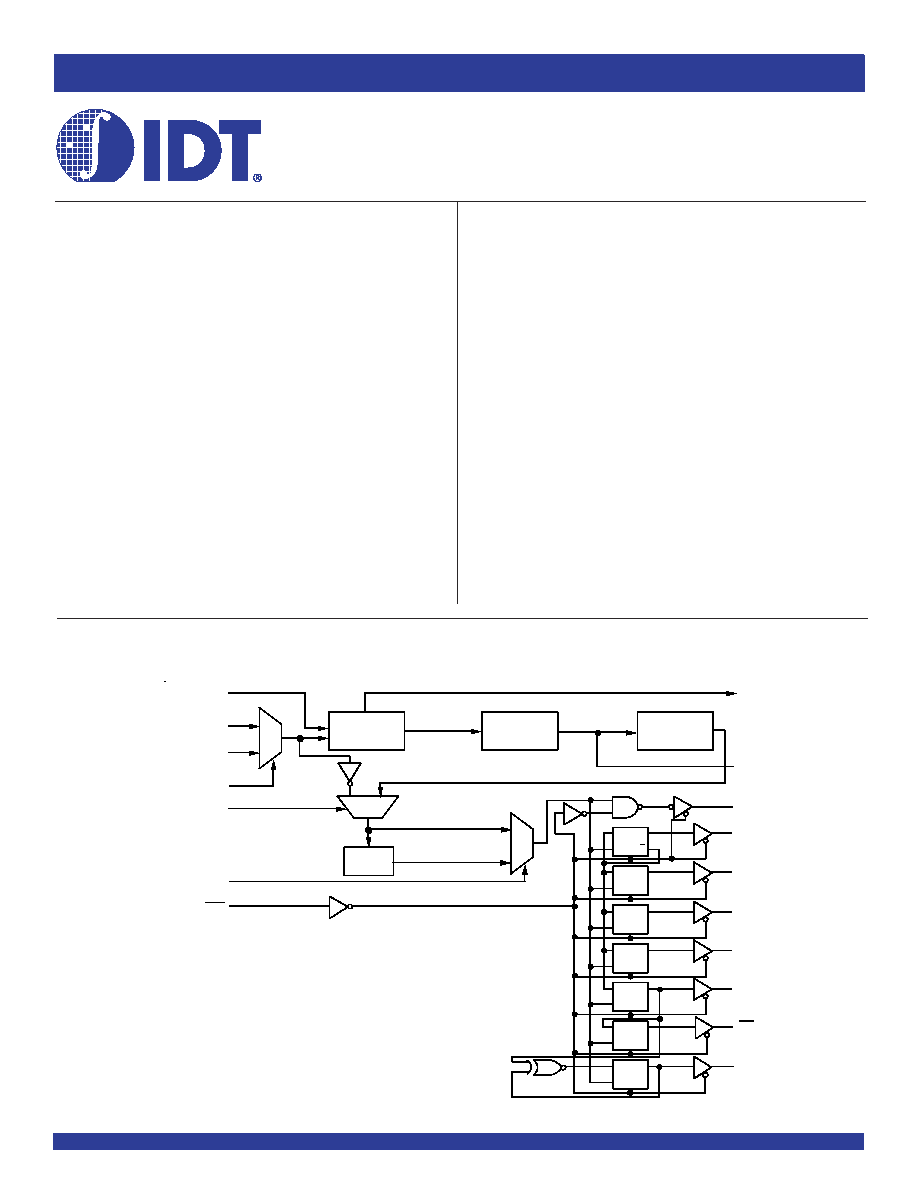
FUNCTIONAL BLOCK DIAGRAM
IDT74FCT388915T
70/100/133/150
3.3V LOW SKEW PLL-BASED
CMOS CLOCK DRIVER
(WITH 3-STATE)
DESCRIPTION:
The FCT388915T uses phase-lock loop technology to lock the fre-
quency and phase of outputs to the input reference clock. It provides low
skew clock distribution for high performance PCs and workstations. One of
the outputs is fed back to the PLL at the FEEDBACK input resulting in
essentially zero delay across the device. The PLL consists of the phase/
frequency detector, charge pump, loop filter and VCO. The VCO is
designed for a 2Q operating frequency range of 40MHz to f2Q Max.
The FCT388915T provides 8 outputs, the Q5 output is inverted from the
Q outputs. The 2Q runs at twice the Q frequency and Q/2 runs at half the
Q frequency.
The FREQ_SEL control provides an additional ˜ 2 option in the output
path. PLL _EN allows bypassing of the PLL, which is useful in static test
modes. When PLL_EN is low, SYNC input may be used as a test clock. In
this test mode, the input frequency is not limited to the specified range and
the polarity of outputs is complementary to that in normal operation (PLL_EN
= 1). The LOCK output attains logic HIGH when the PLL is in steady-state
phase and frequency lock. When OE/RST is low, all the outputs are put in
high impedance state and registers at Q, Q and Q/2 outputs are reset.
The FCT388915T requires one external loop filter component as
recommended in Figure 3.
Phase/Freq.
Detector
M
u
x
0
1
SYNC (0)
FEED BAC K
SYNC (1)
REF_SEL
PLL_EN
M ux
0
1
Divide
-By-2
(
˜
1)
(
˜
2)
1
0
M
u
x
Charge Pum p
Voltage
Controlled
Oscilator
OE/RST
FREQ_SEL
2Q
Q0
Q1
Q2
Q3
Q4
Q5
Q/2
R
D
Q
C P
Q
LF
LOCK
R
D
Q
C P
R
D
Q
C P
R
D
Q
C P
R
D
Q
C P
R
D
Q
C P
R
D
Q
C P

COMMERCIAL TEMPERATURE RANGE
2
IDT74FCT388915T
3.3V LOW SKEW PLL-BASED CMOS CLOCK DRIVER (3-STATE)
PIN CONFIGURATION
PIN DESCRIPTION
O
E
/
R
S
T
V
C
C
Q
5
G
N
D
Q
4
V
C
C
2
Q
Q/2
GND
Q3
V
CC
Q2
GND
LOCK
P
L
L
_
E
N
G
N
D
Q
1
V
C
C
Q
0
G
N
D
F
R
E
Q
_
S
E
L
FEEDBK
REF_SEL
SYNC(0)
V
CC
(AN)
LF
GND(AN)
SYNC(1)
28
4
3
2
1
27
26
25
24
23
22
21
20
19
5
6
7
8
9
10
11
12
13
14
15
16
17
18
5
6
7
8
9
10
V
CC
OE/RST
FEEDBACK
1
2
3
4
20
19
18
17
16
15
14
13
Q4
12
11
GND
Q/2
REF_SEL
SYNC(0)
V
CC
(AN)
LF
V
CC
GND
Q3
V
CC
Q2
GND
GND(AN)
LOCK
Q5
2Q
21
22
23
24
SYNC(1)
FREQ_SEL
GND
Q0
V
CC
Q1
GND
PLL_EN
25
26
27
28
SSOP
TOP VIEW
PLCC
TOP VIEW
Pin Name
I/O
Description
SYNC(0)
I
Reference clock input
SYNC(1)
I
Reference clock input
REF_SEL
I
Chooses reference between SYNC (0) & SYNC (1) (refer to functional block diagram)
FREQ_SEL
I
Selects between ˜ 1 and ˜ 2 frequency options (refer to functional block diagram)
FEEDBACK
I
Feedback input to phase detector
LF
I
Input for external loop filter connection
Q0-Q4
O
Clock output
Q5
O
Inverted clock output
2Q
O
Clock output (2 x Q frequency)
Q/2
O
Clock output (Q frequency ˜ 2)
LOCK
O
Indicates phase lock has been achieved (HIGH when locked)
OE/RST
I
Asynchronous reset (active LOW) and output enable (active HIGH). When HIGH, outputs are enabled. When LOW, outputs are in
HIGH impedance.
PLL_EN
I
Disables phase-lock for low frequency testing (refer to functional block diagram)
COMMERCIAL TEMPERATURE RANGE
IDT74FCT388915T
3.3V LOW SKEW PLL-BASED CMOS CLOCK DRIVER (3-STATE)
3
Symbol
Description
Max
Unit
V
TERM
(2)
Terminal Voltage with Respect to GND
≠0.5 to +4.6
V
V
TERM
(3)
Terminal Voltage with Respect to GND
≠0.5 to +7
V
V
TERM
(4)
Terminal Voltage with Respect to GND
≠0.5 to V
CC
+0.5
V
T
STG
Storage Temperature
≠65 to +150
∞C
I
OUT
DC Output Current
≠60 to +120
mA
ABSOLUTE MAXIMUM RATINGS
(1)
NOTES:
1. Stresses greater than those listed under ABSOLUTE MAXIMUM RATINGS may cause
permanent damage to the device. This is a stress rating only and functional operation
of the device at these or any other conditions above those indicated in the operational
sections of this specification is not implied. Exposure to absolute maximum rating
conditions for extended periods may affect reliability.
2. Vcc terminals.
3. Input terminals.
4. Outputs and I/O terminals.
Symbol
Parameter
Conditions
Typ.
Max.
Unit
C
IN
Input Capacitance
V
IN
= 0V
4.5
6
pF
C
OUT
Output Capacitance
V
OUT
= 0V
5.5
8
pF
CAPACITANCE
(T
A
= +25∞C, F = 1.0MHz)
Symbol
Parameter
Test Conditions
(1)
Min.
Typ.
(2)
Max.
Unit
V
IH
Input HIGH Level
Guaranteed Logic HIGH Level
2
--
--
V
V
IL
Input LOW Level
Guaranteed Logic LOW Level
--
--
0.8
V
I
IH
Input HIGH Current
(4)
V
CC
= Max.
V
I
= 5.5V
--
--
±1
µA
I
IL
Input LOW Current
(4)
V
CC
= Max.
V
I
= GND
--
--
±1
µA
I
OZH
High Impedance Output Current
(4)
V
CC
= Max.
V
I
= V
CC
--
--
±1
µA
I
OZL
(3-State Output Pins)
V
I
= GND
--
--
±1
V
IK
Clamp Diode Voltage
V
CC
= Min., I
IN
= ≠18mA
--
≠0.7
≠1.2
V
I
ODH
Output Drive Current
V
CC
= Min., V
IN
= V
IH
or V
IL,
V
O
= 1.5V
(3)
≠36
--
--
mA
I
ODL
Output Drive Current
V
CC
= Min., V
IN
= V
IH
or V
IL,
V
O
= 1.5V
(3)
50
--
--
mA
V
OH
Output HIGH Voltage
V
CC
= Min
I
OH
= ≠16mA
2.4
(4)
3.3
--
V
V
OL
Output LOW Voltage
V
CC
= Min
I
OL
= 32mA
--
0.3
0.5
V
V
H
Input Hysteresis
--
--
100
--
mV
I
CCL
Quiescent Power Supply Current
V
CC
= Max.,V
IN
= GND or V
CC
--
2
6
µA
I
CCH
(Test Mode)
I
CCZ
DC ELECTRICAL CHARACTERISTICS OVER OPERATING RANGE
Following Conditions Apply Unless Otherwise Specified:
Commercial: T
A
= 0∞C to +70∞C, V
CC
= 3.3V ± 0.3V
NOTES:
1. For conditions shown as Min. or Max., use appropriate value specified under Electrical Characteristics for the applicable device type.
2. Typical values are at V
CC
= 3.3V, +25∞C ambient.
3. Not more than one output should be tested at one time. Duration of the test should not exceed one second.
4. V
OH
= V
CC
- 0.6V at rated current.

COMMERCIAL TEMPERATURE RANGE
4
IDT74FCT388915T
3.3V LOW SKEW PLL-BASED CMOS CLOCK DRIVER (3-STATE)
POWER SUPPLY CHARACTERISTICS
Symbol
Parameter
Test Conditions
(1)
Min.
Typ.
(2)
Max.
Unit
I
CC
Quiescent Power Supply Current
V
CC
= Max.
V
IN
= V
CC
≠0.6V
(3)
--
2
30
µA
TTL Inputs HIGH
V
IN
= V
CC
≠2.1V
(3)
I
CCD
Dynamic Power Supply Current
(4)
V
CC
= Max.
V
IN
= V
CC
--
0.2
0.3
mA/
All Outputs Open
V
IN
= GND
MHz
C
PD
Power Dissipation Capacitance
50% Duty Cycle
--
15
25
pF
I
C
Total Power Supply Current
(6)
V
CC
= Max.
--
30
60
mA
PLL_EN = 1, LOCK = 1, FEEDBACK = Q4
SYNC frequency = 50MHz. All bits loaded with 15pF
V
CC
= Max.
--
90
120
mA
PLL_EN = 1, LOCK = 1, FEEDBACK = Q4
SYNC frequency = 50MHz. All bits loaded with 50
Thevenin
termination and 20pF
NOTES:
1. For conditions shown as Max. or Min., use appropriate value specified under Electrical Characteristics for the applicable device type.
2. Typical values are at V
CC
= 3.3V, +25∞C ambient.
3. Per TTL driven input. All other inputs at V
CC
or GND.
4. This parameter is not directly testable, but is derived for use in Total Power Supply Calculations. It is derived with Q frequency as the reference.
5. Values for these conditions are examples of the I
CC
formula. These limits are guaranteed but not tested.
6. I
C
= I
QUIESCENT
+ I
INPUTS
+ I
DYNAMIC
I
C
= I
CC
+ DI
CC
D
H
N
T
+ I
CCD
(f) + I
LOAD
I
CC
= Quiescent Current (I
CCL
,
I
CCH
and I
CCZ
)
I
CC
= Power Supply Current for a TTL High Input (V
IN
= 3.4V)
D
H
= Duty Cycle for TTL Inputs High
N
T
= Number of TTL Inputs at D
H
I
CCD
= Dynamic Current Caused by an Input Transition Pair (HLH or LHL)
f = 2Q Frequency
I
LOAD
= Dynamic Current due to load.
OUTPUT FREQUENCY SPECIFICATIONS
Max.
(2)
Symbol
Parameter
Min.
70
100
133
(3)
150
(3)
Unit
f2Q
Operating frequency 2Q Output
40
70
100
133
150
MHz
fQ
Operating frequency Q0-Q4, Q5 Outputs
20
35
50
66.7
75
MHz
fQ/2
Operating frequency Q/2 Output
10
17.5
25
33.3
37.5
MHz
SYNCH INPUT TIMING REQUIRMENTS
Symbol
Parameter
Min.
Max.
Unit
T
RISE/FALL
Rise/Fall Times, SYNC inputs
--
3
ns
(0.8V to 2V)
Frequency Input Frequency, SYNC Inputs
10
(1)
2Q fmax MHz
Duty Cycle Input Duty Cycle, SYNC Inputs
25%
75%
--
NOTES:
1. Note 7 in "General AC Specification Notes" and Figure 3 describes this specification and its actual limits depending on the feedback connection.
2. Maximum operating frequency is guaranteed with the part in a phase locked condition and all outputs loaded.
3. At this frequency, 2Q cannot be used as feedback.

COMMERCIAL TEMPERATURE RANGE
IDT74FCT388915T
3.3V LOW SKEW PLL-BASED CMOS CLOCK DRIVER (3-STATE)
5
SWITCHING CHARACTERISTICS OVER OPERATING RANGE
Symbol
Parameter
Condition
(1)
Min.
Max.
Unit
t
RISE/FALL
Rise/Fall Time
Load = 50
to V
CC
/2, C
L
= 20pF
0.2
(2)
2
ns
All Outputs
(between 0.8V and 2V)
t
PULSE WIDTH (3)
Output Pulse Width
Load = 50
to V
CC
/2, C
L
= 20pF
0.5t
CYCLE
≠ 0.8
(5)
0.5t
CYCLE
+ 0.8
(5)
ns
Q, Q, Q/2 outputs
(3)
Q0-Q4, Q5, Q/2, @ 1.5V
t
PULSE WIDTH
Output Pulse Width
0.5t
CYCLE
≠ 1
(5)
0.5t
CYCLE
+ 1
(5)
ns
2Q Output
(3)
2Q @ 1.5V
t
PD
SYNC input to FEEDBACK delay
Load = 50
to V
CC
/2, C
L
= 20pF
+0.3
+1.3
ns
SYNC-FEEDBACK
(3)
(measured at SYNC0 or 1 and FEEDBACK input pins) 0.1µF from LF to Analog GND
(5)
t
SKEW
r
Output to Output Skew between outputs 2Q, Q0-Q4,
Load = 50
to V
CC
/2, C
L
= 20pF
--
600
ps
(rising)
(3,4)
Q/2 (rising edges only)
t
SKEW
f
Output to Output Skew
--
250
ps
(falling)
(3,4)
between outputs Q0-Q4 (falling edges only)
t
SKEW
all
(3,4)
Output to Output Skew
--
800
ps
2Q, Q/2, Q0-Q4 rising, Q5 falling
t
LOCK(6)
Time required to acquire Phase-Lock from time
1
(2)
10
ms
SYNC input signal is received
t
PZH
Output Enable Time
3
(2)
14
ns
t
PZL
OE/RST (LOW-to-HIGH) to Q, 2Q, Q/2, Q
t
PHZ
Output Disable Time
3
(2)
14
ns
t
PLZ
OE/RST (HIGH-to-LOW) to Q, 2Q, Q/2, Q
GENERAL AC SPECIFICATION NOTES:
1. See test circuit and waveforms.
2. Minimum limits are guaranteed but not tested.
3. These specifications are guaranteed but not production tested.
4. Under equally loaded conditions, as specified under test conditions and at a fixed temperature and voltage.
5. t
CYCLE
= 1/frequency at which each output (Q, Q, Q/2 or 2Q) is expected to run.
6. With V
CC
fully powered-on and an output properly connected to the FEEDBACK pin, t
LOCK
Max. is with C1 = 0.1µF, t
LOCK
Min. is with C1 = 0.01µF. (Where C1 is loop filter
capacitor shown in Figure 2).
7. The wiring diagrams and written explanations of Figure 3 demonstrate the input and output frequency relationships for various possible feedback configurations. The allowable
SYNC input range to stay in the phase-locked condition is also indicated. There are two allowable SYNC frequency ranges, depending on whether FREQ_SEL is HIGH or LOW.
Also it is possible to feed back the Q5 output, thus creating a 180∞ phase shift between the SYNC input and the Q outputs. The table below summarizes the allowable SYNC
frequency range for each possible configuration.
FREQ_SEL
Feedback
Allowable SYNC Input
Corresponding 2Q Output
Phase Relationship of the Q Outputs
Level
Output
Frequency Range (MHZ)
Frequency Range
to Rising SYNC Edge
HIGH
Q/2
10 to (2x_Q
f
MAX
Spec)/4
40 to (2Q
f
MAX
Spec)
0∞
HIGH
Any Q (Q0-Q4)
20
to (2x_Q
f
MAX
Spec)/2
40 to (2Q
f
MAX
Spec)
0∞
HIGH
Q5
20
to (2x_Q
f
MAX
Spec)/2
40 to (2Q
f
MAX
Spec)
180∞
HIGH
2X_Q
40
to (2x_Q
f
MAX
Spec)
40 to (2Q
f
MAX
Spec)
0∞
LOW
Q/2
5
to (2x_Q
f
MAX
Spec)/8
20 to (2Q
f
MAX
Spec)/2
0∞
LOW
Any Q (Q0-Q4)
10 to (2x_Q
f
MAX
Spec)/4
20 to (2Q
f
MAX
Spec)/2
0∞
LOW
Q5
10 to (2x_Q
f
MAX
Spec)/4
20 to (2Q
f
MAX
Spec)/2
180∞
LOW
2X_Q
20
to (2x_Q
f
MAX
Spec)/2
20 to (2Q
f
MAX
Spec)/2
0∞

COMMERCIAL TEMPERATURE RANGE
6
IDT74FCT388915T
3.3V LOW SKEW PLL-BASED CMOS CLOCK DRIVER (3-STATE)
GENERAL AC SPECIFICATION NOTES (continued):
8. The tPD spec describes how the phase offset between the SYNC input and the output connected to the FEEDBACK input, varies with process, temperature and voltage. The
phase measurements were made at 1.5V. The Q/2 output was terminated at the FEEDBACK input with 100
to V
CC
and 100
to ground. tPD measurements were made with
the loop filter connection shown in Figure 1 below:
Analog loop filter section
of the FC T388915T
ANALO G V
C C
ANALO G G ND
LF
BO ARD G ND
BO AR D V
C C
0.1
µ
F (Loop
Filter Cap)
0.1
µ
F
High
Freq.
Bypass
10
µ
F
Low
Freq.
Bypass
A separate Analog power supply is not necessary
and should not be used. Following these pre-
scribed guidelines is all that is necessary to use
the FCT388915T in a normal digital environm ent.
LF
Exte rnal Loop
Filter
0.1
µ
F
C 1
Analog G ND
Figure 2. Recommended Loop Filter and Analog Isolation Scheme for the FCT388915T
NOTES:
1. Figure 2 shows a loop filter and analog isolation scheme which will be effective in most applications. The following guidelines should be followed to ensure stable and jitter-free
operation:
a. All loop filter and analog isolation components should be tied as close to the package as possible. Stray current passing through the parasitics of long traces can cause undesirable
voltage transients at the LF pin.
b. The 10µF low frequency bypass capacitor and the 0.1µF high frequency bypass capacitor form a wide bandwidth filter that will minimize the 388915T's sensitivity to voltage
transients from the system digital V
CC
supply and ground planes.
If good bypass techniques are used on a board design near components which may cause digital V
CC
and ground noise, V
CC
step deviations should not occur at the 388915T's
digital V
CC
supply. The purpose of the bypass filtering scheme shown in figure 2 is to give the 388915T additional protection from the power supply and ground plane transients
that can occur in a high frequency, high speed digital system.
c. The loop filter capacitor (0.1µF) can be a ceramic chip capacitor, the same as a standard bypass capacitor.
2. In addition to the bypass capacitors used in the analog filter of Figure 2 there should be a 0.1µF bypass capacitor between each of the other (digital) four V
CC
pins and the board
ground plane. This will reduce output switching noise caused by the 388915T outputs, in addition to reducing potential for noise in the "analog" section of the chip. These bypass
capacitors should also be tied as close to the 388915T package as possible.
Figure 1

COMMERCIAL TEMPERATURE RANGE
IDT74FCT388915T
3.3V LOW SKEW PLL-BASED CMOS CLOCK DRIVER (3-STATE)
7
The frequency relationship shown here is applicable to all Q outputs (Q0, Q1,
Q2, Q3 and Q4).
1:2 INPUT TO "Q" OUTPUT
FREQUENCY RELATIONSHIP
In this application, the Q/2 output is connected to the FEEDBACK input. The
internal PLL will line up the positive edges of Q/2 and SYNC, thus the Q/2
frequency will equal the SYNC frequency. The Q outputs (Q0-Q4, Q5) will
always run at 2X the Q/2 frequency, and the 2Q output will run at 4X the Q/2
frequency.
1:1 INPUT TO "Q" OUTPUT
FREQUENCY RELATIONSHIP
In this application, the Q4 output is connected to the FEEDBACK input. The
internal PLL will line up the positive edges of Q4 and SYNC, thus the Q4
frequency (and the rest of the "Q" outputs) will equal the SYNC frequency. The
Q/2 output will always run at 1/2 the Q frequency, and the 2Q output will run
at 2X the Q frequency.
Allowable Input Frequency Range:
40MHz to (f2Q MAX Spec) (for FREQ_SEL HIGH)
20MHz to (f2Q MAX Spec)/2 (for FREQ_SEL LOW)
Allowable Input Frequency Range:
20MHz to (f2Q MAX Spec)/2 (for FREQ_SEL HIGH)
10MHz to (f2Q MAX Spec)/4 (for FREQ_SEL LOW)
2:1 INPUT TO "Q" OUTPUT
FREQUENCY RELATIONSHIP
In this application, the 2Q output is connected to the FEEDBACK input. The
internal PLL will line up the positive edges of 2Q and SYNC, thus the 2Q
frequency will equal the SYNC frequency. The Q/2 output will always run at
1/4 the 2Q frequency, and the Q output will run at 1/2 the 2Q frequency.
Figure 3a. Wiring Diagram and Frequency Relationships With Q/
2 Output Feedback
Figure 3c. Wiring Diagram and Frequency Relationships With
2Q Output Feedback
Figure 3b. Wiring Diagram and Frequency Relationships With
Q4 Output Feedback
Allowable Input Frequency Range:
10MHz to ( f2Q MAX Spec)/4 (for FREQ_SEL HIGH)
5MHz to (f2Q MAX Spec)/8 (for FREQ_SEL LOW)
Q/2
Q3
Q2
PLL_EN
Q1
Q0
FQ_SEL
FEED BAC K
REF_SEL
SYNC(0)
V
C C
(AN)
GN D(AN)
Q4
Q5
2Q
LOW
50 M Hz signal
12.5 M Hz feedback signal
HIGH
HIGH
HIGH
25 MHz
"Q"
C lock
Outputs
12.5 MHz
input
LF
FC T388915T
RST
OE/
Q/2
Q3
Q2
PLL_EN
Q1
Q 0
FQ_SEL
FEED BAC K
REF_SEL
SYNC (0)
V
CC
(AN)
GN D(AN )
Q4
Q5
2Q
LOW
50 M H z signal
25 M Hz feedback signal
HIGH
HIGH
H IGH
25 M Hz
"Q"
C lock
O utputs
25 M H z
input
12.5 M Hz
signal
LF
FC T388915T
RST
OE/
Q/2
Q3
Q2
PLL_EN
Q1
Q0
FQ_SEL
FEED BACK
REF_SEL
SYNC(0)
V
CC
(AN)
GND(AN)
Q4
Q5
2Q
LOW
50 M Hz feedback signal
HIGH
HIGH
HIGH
25 M Hz
"Q"
Clock
Outputs
50 M Hz
input
12.5 MHz
input
LF
FCT388915T
RST
OE/
COMMERCIAL TEMPERATURE RANGE
8
IDT74FCT388915T
3.3V LOW SKEW PLL-BASED CMOS CLOCK DRIVER (3-STATE)
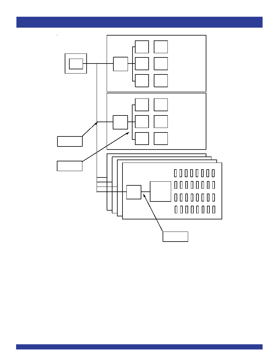
CM M U
CM MU
CPU
CM MU
CM M U
CM MU
CM M U
CM MU
CPU
CM MU
CM M U
CM MU
PLL
2f
PLL
2f
CPU
CARD
CPU
CARD
CLOCK
@ f
SYSTEM
CLO CK
SO UR CE
FCT388915T
FCT388915T
DISTRIBUTE
CLO CK @ f
CLOCK @ 2f
at point of use
M EM O RY
CO NTROL
PLL
2f
M EM O RY
CAR DS
CLOCK @ 2f
at point of use
FCT388915T
Figure 4. Multiprocessing Application Using the FCT388915T for Frequency Multiplication
and Low Board-to-Board skew
FCT388915T SYSTEM LEVEL TESTING
FUNCTIONALITY
When the PLL_EN pin is LOW, the PLL is bypassed and the FCT388915T
is in low frequency "test mode". In test mode (with FREQ_SEL HIGH), the 2Q
output is inverted from the selected SYNC input, and the Q outputs are divide-
by-2 (negative edge triggered) of the SYNC input, and the Q/2 output is divide-
by-4 (negative edge triggered). With FREQ_SEL LOW the 2Q output is divide-
by-2 of the SYNC, the Q outputs divide-by-4, and the Q/2 output divide-by-8.
These relationships can be seen in the block diagram. A recommended test
configuration would be to use SYNC0 or SYNC1 as the test clock input, and tie
PLL_EN and REF_SEL together and connect them to the test select logic.
This functionality is needed since most board-level testers run at 1 MHz or
below, and theFCT 388915T cannot lock onto that low of an input frequency.
In the test mode described above, any test frequency test can be used.

COMMERCIAL TEMPERATURE RANGE
IDT74FCT388915T
3.3V LOW SKEW PLL-BASED CMOS CLOCK DRIVER (3-STATE)
9
t
S YNC IN PUT
t
"Q" OUTPUTS
t
t
t
t
t
P D
SYNC IN PUT
(SYNC (1) or
SYNC (0))
FEED BAC K
INPUT
Q/2 OUTPUT
Q0-Q4
OUTPUTS
Q5 OUTPUT
2Q OUTPUT
t
SKEW f
SKEW r
SKEW f
S KEW ALL
S KEW r
CYCLE
CYCLE
1.5V
V
CC /2
V
C C /2
V
CC /2
V
CC /2
V
CC /2
CONTROL
INPUT
3V
1.5V
0V
3V
0V
OUTP UT
NORM ALLY
LOW
OUTP UT
NORM ALLY
HIGH
SW ITCH
6V
SW ITCH
GND
V
OL
0.3V
0.3V
t
PLZ
t
PZL
t
PZH
t
PHZ
3V
0V
1.5V
1.5V
ENA BLE
D ISAB LE
V
O H
Pulse
Generator
D.U.T.
V
C C
V
IN
V
OU T
100
100
R
T
V
CC
20pF
C
L
P ulse
Generator
D.U.T.
V
C C
V
IN
V
OU T
500
GND
6.0V
500
R
T
(These waveforms represent the configuration of Figure 3a)
NOTES:
1. The FCT388915T aligns rising edges of the FEEDBACK input and SYNC input, therefore the SYNC input does not require a 50% duty cycle.
2. All skew specs are measured between the V
CC
/2 crossing point of the appropriate output edges. All skews are specified as "windows", not as ± deviation around a center point.
3. If a Q ouput is connected to the FEEDBACK input (this situation is not shown), the Q output frequency would match the SYNC input frequency, the 2Q output would run at twice
the SYNC frequency and the Q/2 output would run at half the SYNC frequency.
Propagation Delay, Output Skew
TEST CIRCUITS AND WAVEFORMS
Test
Switch
Disable Low
6V
Enable Low
Disable High
GND
Enable High
SWITCH POSITION
DEFINITIONS:
C
L
= Load capacitance: includes jig and probe capacitance.
R
T
= Termination resistance: should be equal to Z
OUT
of the Pulse Generator.
NOTES:
1. Diagram shown for input Control Enable-LOW and input Control Disable-HIGH.
2. Pulse Generator for All Pulses: t
F
2.5ns; t
R
2.5ns.
Enable and Disable Times
Enable and Disable Test Circuit
50
to V
CC
/2, C
L
= 20pF

COMMERCIAL TEMPERATURE RANGE
10
IDT74FCT388915T
3.3V LOW SKEW PLL-BASED CMOS CLOCK DRIVER (3-STATE)
ORDERING INFORMATION
XXXX
Device Type
Package
J
PY
388915T
PLCC
SSOP
3.3V Low skew PLL-based CMOS clock driver
XX
Speed
70
100
133
150
70MHz Max. Frequency
100MHz Max. Frequency
133MHz Max. Frequency
150MHz Max. Frequency
XX
FCT
IDT
XX
Temp. Range
74
0∞C to +70∞C
CORPORATE HEADQUARTERS
for SALES:
for Tech Support:
2975 Stender Way
800-345-7015 or 408-727-6116
logichelp@idt.com
Santa Clara, CA 95054
fax: 408-492-8674
(408) 654-6459
www.idt.com