 | –≠–ª–µ–∫—Ç—Ä–æ–Ω–Ω—ã–π –∫–æ–º–ø–æ–Ω–µ–Ω—Ç: 74FCT621T | –°–∫–∞—á–∞—Ç—å:  PDF PDF  ZIP ZIP |
INDUSTRIAL TEMPERATURE RANGE
IDT74FCT621T/AT
FAST CMOS OCTAL BUS TRANSCEIVER (OPEN DRAIN)
1
AUGUST 2000
INDUSTRIAL TEMPERATURE RANGE
The IDT logo is a registered trademark of Integrated Device Technology, Inc.
© 2000 Integrated Device Technology, Inc.
DSC-2538/7
FEATURES:
∑ Std. and A grades
∑ Low input and output leakage
1µA (max.)
∑ CMOS power levels
∑ True TTL input and output compatibility:
≠ V
OH
= 3.3V (typ.)
≠ V
OL
= 0.3V (typ.)
∑ Meets or exceeds JEDEC standard 18 specifications
∑ Power off disable outputs permit "live insertion"
∑ Available in SOIC package
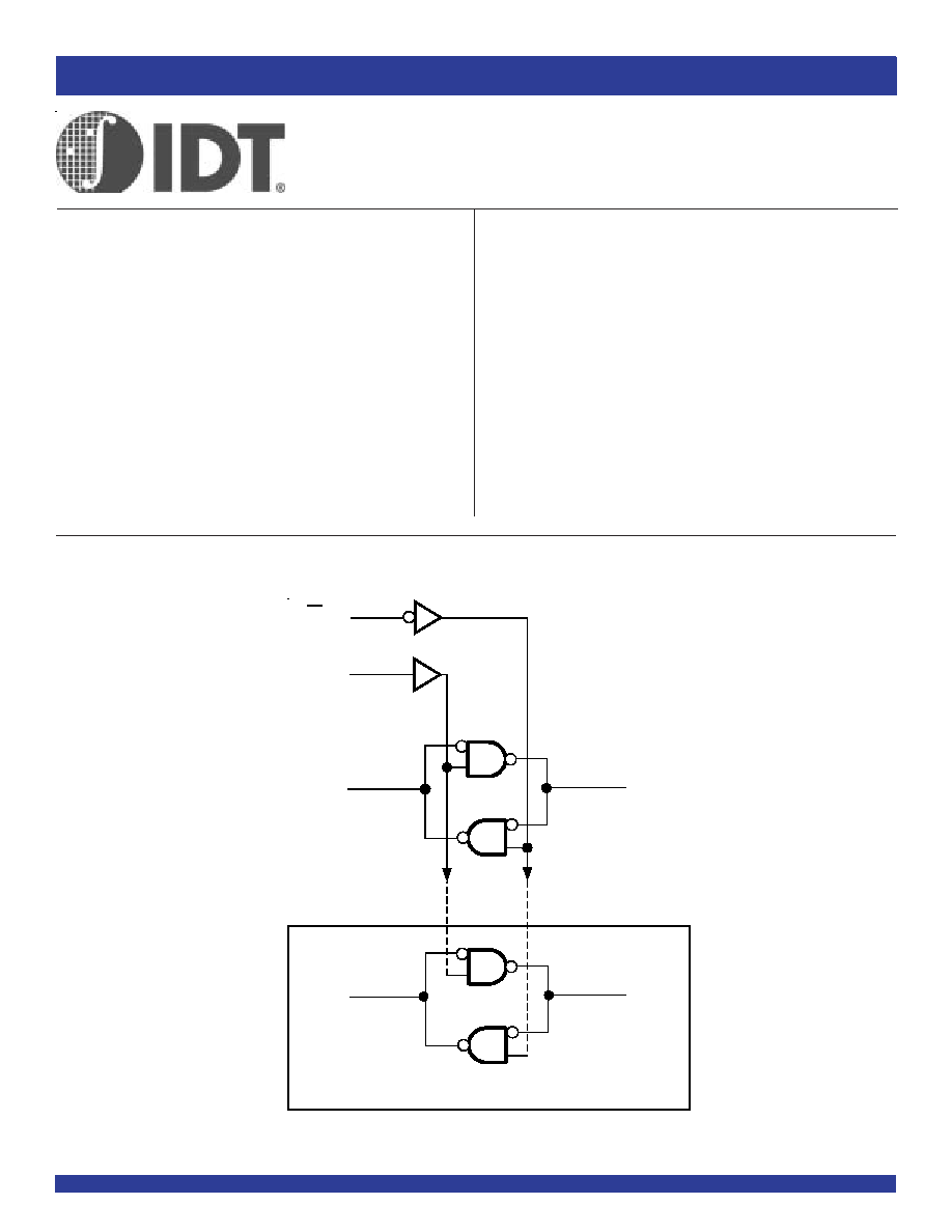
FUNCTIONAL BLOCK DIAGRAM
IDT74FCT621T/AT
FAST CMOS
OCTAL BUS TRANSCEIVER
(OPEN DRAIN)
DESCRIPTION:
The IDT74FCT621T is an octal transceiver with non-inverting Open-
Drain bus compatible outputs in both send and receive directions. The B
bus outputs are capable of sinking 64mA providing very good capacitive
drive characteristics. These octal bus transceivers are designed for
asynchronous two-way communication between data buses. The control
function implementation allows for maximum flexibility in timing.
GBA
GAB
A
1
B
1
A
2
-A
8
B
2
-B
8
SEVEN OTH ER T RANSC EIVERS
2
18
19
1
INDUSTRIAL TEMPERATURE RANGE
2
IDT74FCT621T/AT
FAST CMOS OCTAL BUS TRANSCEIVER (OPEN DRAIN)
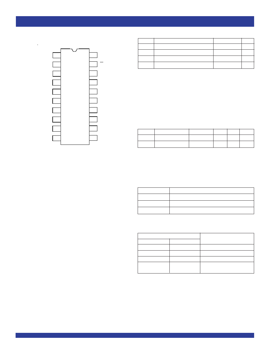
PIN CONFIGURATION
Symbol
Description
Max
Unit
V
TERM
(2)
Terminal Voltage with Respect to GND
≠0.5 to +7
V
V
TERM
(3)
Terminal Voltage with Respect to GND
≠0.5 to V
CC
+0.5
V
T
STG
Storage Temperature
≠65 to +150
∞C
I
OUT
DC Output Current
≠60 to +120
mA
ABSOLUTE MAXIMUM RATINGS
(1)
NOTES:
1. Stresses greater than those listed under ABSOLUTE MAXIMUM RATINGS may cause
permanent damage to the device. This is a stress rating only and functional operation
of the device at these or any other conditions above those indicated in the operational
sections of this specification is not implied. Exposure to absolute maximum rating
conditions for extended periods may affect reliability. No terminal voltage may exceed
Vcc by +0.5V unless otherwise noted.
2. Inputs and Vcc terminals only.
3. Output and I/O terminals only.
Symbol
Parameter
(1)
Conditions
Typ.
Max.
Unit
C
IN
Input Capacitance
V
IN
= 0V
6
10
pF
C
OUT
Output Capacitance
V
OUT
= 0V
8
12
pF
CAPACITANCE
(T
A
= +25∞C, F = 1.0MHz)
NOTE:
1. This parameter is measured at characterization but not tested.
SOIC
TOP VIEW
2
3
1
1 6
1 5
1 4
1 1
1 9
1 8
2 0
1 7
1 3
1 2
5
6
7
4
SO20-2
8
9
1 0
A
2
A
1
V
CC
A
3
A
6
A
4
A
5
A
7
GN D
GBA
B
2
B
8
B
1
B
3
B
6
B
4
B
5
B
7
GAB
A
8
PIN DESCRIPTION
Pin Names
Description
GBA, GAB
Enable Inputs
A
1
≠ A
8
A Inputs or Open-drain Outputs
B
1
≠ B
8
B Inputs or Open-drain Outputs
FUNCTION TABLE
(1)
Enable Inputs
GBA
GAB
Function
L
L
B data to A bus
H
H
A data to B bus
H
L
OFF
L
H
B data to A bus
A data to B bus
NOTE:
1. H = HIGH Voltage Level.
L = LOW Voltage Level.
OFF = HIGH if pull-up resistor is connected to Open-Drain output.
INDUSTRIAL TEMPERATURE RANGE
IDT74FCT621T/AT
FAST CMOS OCTAL BUS TRANSCEIVER (OPEN DRAIN)
3
DC ELECTRICAL CHARACTERISTICS OVER OPERATING RANGE
Following Conditions Apply Unless Otherwise Specified:
Industrial: T
A
= ≠40∞C to +85∞C, V
CC
= 5.0V ±5%
Symbol
Parameter
Test Conditions
(1)
Min.
Typ.
(2)
Max.
Unit
V
IH
Input HIGH Level
Guaranteed Logic HIGH Level
2
--
--
V
V
IL
Input LOW Level
Guaranteed Logic LOW Level
--
--
0.8
V
I
IH
Input HIGH Current
(4)
V
CC
= Max., V
I
= 2.7V
--
--
±1
µA
I
IL
Input LOW Current
(4)
V
CC
= Max., V
I
= 0.5V
--
--
±1
µA
I
I
Input HIGH Current
(4)
V
CC
= Max., V
I
= V
CC
(Max.)
--
--
±1
µA
V
IK
Clamp Diode Voltage
V
CC
= Min., I
N
= ≠18mA
--
≠0.7
≠1.2
V
I
OH
Output HIGH Current
V
CC
= Max.
V
OH
= Vcc (Max.)
--
--
20
µA
V
IN
= V
IH
or V
IL
V
OL
Output LOW Voltage
V
CC
= Min.
I
OL
= 64mA
(3)
--
0.3
0.55
V
(B Bus)
V
IN
= V
IH
or V
IL
V
OL
Output LOW Voltage
V
CC
= Min.
I
OL
= 48mA
(3)
--
0.3
0.5
V
(A Bus)
V
IN
= V
IH
or V
IL
I
OFF
Input/Output Power Off
V
CC
= 0V, V
IN
or V
O
- 4.5V
--
--
±1
µA
Leakage
(4)
V
H
Input Hysteresis
--
--
200
--
mV
I
CC
Quiescent Power Supply
V
CC
= max., V
IN
= GND or Vcc
--
0.01
1
mA
Current
NOTES:
1. For conditions shown as Max. or Min., use appropriate value specified under Electrical Characteristics for the applicable device type.
2. Typical values are at V
CC
= 5.0V, +25∞C ambient.
3. These are maximum I
OL
values per output, for 8 outputs turned on simultaneously. Total maximum I
OL
(all outputs) is 512mA for commercial and 384mA for military. Derate
I
OL
for number of outputs exceeding 8 turned on simultaneously.
4. The test limit for this parameter is ±5µA at T
A
= ≠55∞C.
INDUSTRIAL TEMPERATURE RANGE
4
IDT74FCT621T/AT
FAST CMOS OCTAL BUS TRANSCEIVER (OPEN DRAIN)
NOTES:
1. See test circuit and waveforms.
2. Minimum limits are guaranteed but not tested on Propagation Delays.
IDT74FCT621T
IDT74FCT621AT
Symbol
Parameter
Condition
(1)
Min.
(2)
Max.
Min.
(2)
Max.
Unit
t
PLH
Propagation Delay, A to B
C
L
= 50pF
5.5
13
5.5
12
ns
t
PHL
R
L
= 500
1.5
8.5
1.5
6.8
t
PLH
Propagation Delay, B to A
5.5
12.5
5.5
12
ns
t
PHL
1.5
8
1.5
6.4
t
PLH
Propagation Delay, GBA to A
5.5
14
5.5
13
ns
t
PHL
1.5
8.5
1.5
6.8
t
PLH
Propagation Delay, GAB to B
5.5
14
5.5
13
ns
t
PHL
1.5
8
1.5
6.4
SWITCHING CHARACTERISTICS OVER OPERATING RANGE
POWER SUPPLY CHARACTERISTICS
Symbol
Parameter
Test Conditions
(1)
Min.
Typ.
(2)
Max.
Unit
I
CC
Quiescent Power Supply Current
V
CC
= Max.
--
0.5
2
mA
TTL Inputs HIGH
V
IN
= 3.4V
(3)
I
CCD
Dynamic Power Supply Current
(4)
Vcc = Max.
V
IN
= V
CC
--
0.15
0.25
mA/MHz
Outputs Open
V
IN
= GND
GBA = GAB = GND or V
CC
One Input Toggling
50% Duty Cycle
I
C
Total Power Supply Current
(6,7)
Vcc = Max.
V
IN
= V
CC
--
1.5
3.5
mA
Outputs Open
V
IN
= GND
GBA = GAB = GND or V
CC
One Bit Toggling
V
IN
= 3.4V
--
1.8
4.5
at f
i
=10MHz
V
IN
= GND
50% Duty Cycle
Vcc = Max.
V
IN
= V
CC
--
3
6
(5)
Outputs Open
V
IN
= GND
GBA = GAB = GND or V
CC
Eight Bits Toggling
V
IN
= 3.4V
--
5
14
(5)
at f
i
= 2.5MHz
V
IN
= GND
50% Duty Cycle
NOTES:
1. For conditions shown as Max. or Min., use appropriate value specified under Electrical Characteristics for the applicable device type.
2. Typical values are at V
CC
= 5.0V, +25∞C ambient.
3. Per TTL driven input (V
IN
= 3.4V); all other inputs at V
CC
or GND.
4. This parameter is not directly testable, but is derived for use in Total Power Supply Calculations.
5. Values for these conditions are examples of the I
CC
formula. These limits are guaranteed but not tested.
6. I
C
= I
QUIESCENT
+ I
INPUTS
+ I
DYNAMIC
I
C
= I
CC
+
I
CC
D
H
N
T
+ I
CCD
(f
CP
/2 + f
i
N
i
)
I
CC
= Quiescent Current
I
CC
= Power Supply Current for a TTL High Input (V
IN
= 3.4V)
D
H
= Duty Cycle for TTL Inputs High
N
T
= Number of TTL Inputs at D
H
I
CCD
= Dynamic Current Caused by an Output Transition Pair (HLH or LHL)
f
CP
= Clock Frequency for Register Devices (Zero for Non-Register Devices)
f
i
= Input Frequency
N
i
= Number of Inputs at f
i
All currents are in milliamps and all frequencies are in megahertz.
7. This test is performed with outputs tied to GND through a pull-down resistor.
INDUSTRIAL TEMPERATURE RANGE
IDT74FCT621T/AT
FAST CMOS OCTAL BUS TRANSCEIVER (OPEN DRAIN)
5
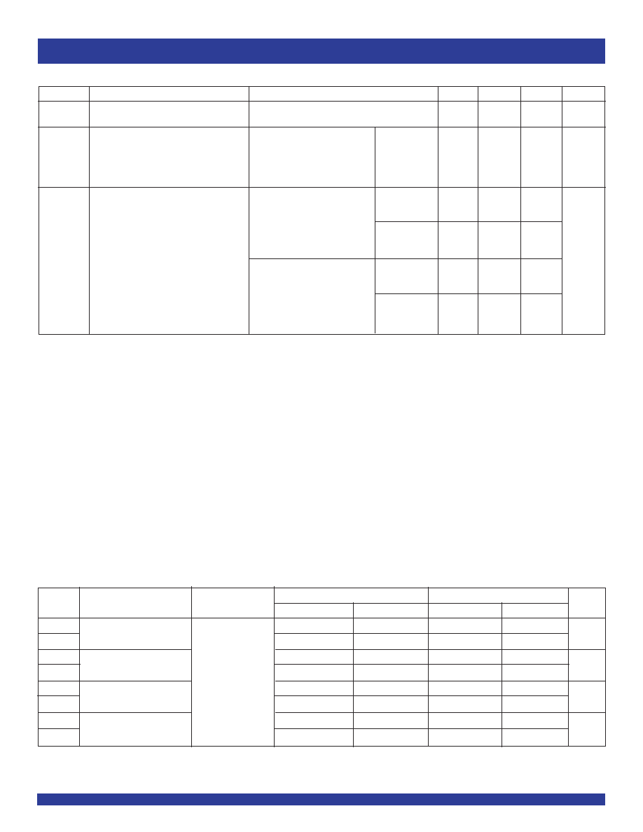
Pulse
G enerator
R
T
D .U .T.
V
C C
V
IN
C
L
V
O UT
50pF
500
500
7.0V
3V
1.5V
0V
3V
1.5V
0V
3V
1.5V
0V
3V
1.5V
0V
DATA
IN PUT
TIM ING
INPU T
ASYNC HR O NOU S C ON TROL
PRES ET
C LEA R
ETC.
SYN CH RON OUS C ON TR OL
t
SU
t
H
t
R E M
t
SU
t
H
HIG H-LOW -H IGH
PU LS E
LOW -HIGH -LOW
PU LS E
t
W
1.5V
1.5V
SAM E PHA SE
IN PU T TR ANSITIO N
3V
1.5V
0V
1.5V
V
OH
t
PL H
O UTPU T
OPPOS ITE PH ASE
IN PU T TR ANSITIO N
3V
1.5V
0V
t
P LH
t
PH L
t
PH L
V
OL
CON TRO L
IN PUT
3V
1.5V
0V
3.5V
0V
OU TPUT
NO RM ALLY
LOW
OU TPUT
NO RM ALLY
HIGH
SW ITC H
C LOSE D
SW ITCH
OPEN
V
O L
0.3V
0.3V
t
PLZ
t
PZL
t
P ZH
t
PH Z
3.5V
0V
1.5V
1.5V
ENAB LE
D ISA BLE
V
O H
PRES ET
C LEA R
CLOCK ENABLE
ETC.
Octal link
Octal link
Octal link
Octal link
Octal link
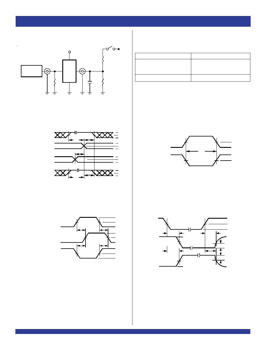
TEST CIRCUITS AND WAVEFORMS
Propagation Delay
Test Circuits for All Outputs
Enable and Disable Times
Set-Up, Hold, and Release Times
Pulse Width
NOTES:
1. Diagram shown for input Control Enable-LOW and input Control Disable-HIGH.
2. Pulse Generator for All Pulses: Rate
1.0MHz; t
F
2.5ns; t
R
2.5ns.
Test
Switch
Open Drain
Disable Low
Closed
Enable Low
All Other Tests
Open
SWITCH POSITION
DEFINITIONS:
C
L
= Load capacitance: includes jig and probe capacitance.
R
T
= Termination resistance: should be equal to Z
OUT
of the Pulse Generator.
INDUSTRIAL TEMPERATURE RANGE
6
IDT74FCT621T/AT
FAST CMOS OCTAL BUS TRANSCEIVER (OPEN DRAIN)
ORDERING INFORMATION
CORPORATE HEADQUARTERS
for SALES:
for Tech Support:
2975 Stender Way
800-345-7015 or 408-727-6116
logichelp@idt.com
Santa Clara, CA 95054
fax: 408-492-8674
(408) 654-6459
www.idt.com
XX
Tem perature Range
X
Package
SO
Sm all Outline IC (SO20-2)
621T
621AT
Octal Bus Transceiver (Open D rain)
-
40
∞
C to +85
∞
C
74
X
DeviceType
IDT
FCT