
1
INDUSTRIAL TEMPERATURE RANGE
IDT74FST1632861
20-BIT, TWO PORT BUS SWITCH WITH RESISTOR
NOVEMBER 1999
INDUSTRIAL TEMPERATURE RANGE
The IDT logo is a registered trademark of Integrated Device Technology, Inc.
© 1999 Integrated Device Technology, Inc.
DSC-5582/1
FEATURES:
∑ Bus switches provide zero delay paths
∑ Low switch on-resistance: 28
∑ TTL-compatible input and output levels
∑ ESD > 2000V per MIL-STD-883, Method 3015; > 200V using
machine model (C = 200pF, R = 0)
∑ Hot insertion capability
∑ Very low power dissipation
∑ Available in SSOP, TSSOP, and TVSOP packages
FUNCTIONAL BLOCK DIAGRAM
IDT74FST1632861
20-BIT, TWO PORT BUS
SWITCH WITH RESISTOR
DESCRIPTION:
The FST1632861 belongs to IDT's family of Bus switches. Bus switch
devices perform the function of connecting or isolating two ports without
providing any inherent current sink or source capability. They generate
little or no noise of their own while providing a low resistance path for an
external driver. These devices connect input and output ports through an
n-channel FET. When the gate-to-source junction of this FET is adequately
forward-biased, the device conducts and the resistance between input and
output ports is small. With-out adequate bias on the gate-to-source junction
of the FET, the FET is turned off, therefore with no V
CC
applied, the device
has hot insertion capability.
The FST1632861 bus switch has a built-in 28
series resistor to reduce
noise which can result from reflections. This 28
built-in series resistor
eliminates the need for an external terminating resistor.
1
OE
A
0
A
1
A
2
A
3
B
0
B
1
B
2
B
3
A
4
A
5
A
6
A
7
B
4
B
5
B
6
B
7
A
8
A
9
B
8
B
9
2
OE
A
10
A
11
A
12
A
13
B
10
B
11
B
12
B
13
A
14
A
15
A
16
A
17
B
14
B
15
B
16
B
17
A
18
A
19
B
18
B
19
2
INDUSTRIAL TEMPERATURE RANGE
IDT74FST1632861
20-BIT, TWO PORT BUS SWITCH WITH RESISTOR
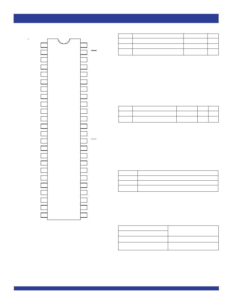
SSOP/ TSSOP/ TVSOP
TOP VIEW
PIN CONFIGURATION
Symbol
Description
Max
Unit
V
TERM
(2)
Terminal Voltage with Respect to GND
≠0.5 to +7
V
T
STG
Storage Temperature
≠65 to +150
∞C
I
OUT
Maximum Continuous Channel Current
128
mA
ABSOLUTE MAXIMUM RATINGS
(1)
NOTES:
1. Stresses greater than those listed under ABSOLUTE MAXIMUM RATINGS may cause
permanent damage to the device. This is a stress rating only and functional operation
of the device at these or any other conditions above those indicated in the operational
sections of this specification is not implied. Exposure to absolute maximum rating
conditions for extended periods may affect reliability.
2. Vcc, Control, and Switch terminals.
Symbol
Parameter
Conditions
(2)
Typ. Unit
C
IN
Control Input Capacitance
6
pF
C
I/O
Switch Input/Output Capacitance
Switch Off
12
pF
CAPACITANCE
(1)
NOTES:
1. Capacitance is characterized but not tested.
2. T
A
= 25∞C, f = 1MHz, V
IN
= 0V, V
OUT
= 0V.
A
0
A
2
A
3
A
5
A
8
A
10
A
11
A
14
A
17
A
1
A
4
A
6
A
7
A
9
GND
NC
A
12
A
13
A
15
A
18
A
19
A
16
GND
1
OE
V
CC
39
29
30
31
32
33
34
35
36
37
38
25
26
27
28
48
47
41
42
43
44
45
46
40
1
2
3
4
5
6
7
8
9
10
12
13
14
15
16
17
18
19
20
11
21
22
23
24
NC
B
0
B
2
B
3
B
5
B
8
B
10
B
11
B
14
B
17
B
1
B
4
B
6
B
7
B
9
Vcc
2
OE
B
12
B
13
B
15
B
18
B
19
B
16
NOTE:
1. H = HIGH Voltage Level
L = LOW Voltage Level
FUNCTION TABLE
(1)
Inputs
xOE
Outputs
L
Connect A to B
H
Disconnect A from B
Pin Names
Description
xOE
Output Enable Inputs (Active LOW)
A x
A Port Bits
B x
B Port Bits
PIN DESCRIPTION
3
INDUSTRIAL TEMPERATURE RANGE
IDT74FST1632861
20-BIT, TWO PORT BUS SWITCH WITH RESISTOR
Symbol
Parameter
Test Conditions
(1)
Min.
Typ.
(2)
Max.
Unit
V
IH
Control Input HIGH Voltage
Guaranteed Logic HIGH for Control Inputs
2
--
--
V
V
IL
Control Input LOW Voltage
Guaranteed Logic LOW for Control Inputs
--
--
0.8
V
I
IH
Control Input HIGH Current
V
CC
= Max.
V
I
= V
CC
--
--
±1
µA
I
IL
Control Input LOW Current
V
I
= GND
--
--
±1
I
OZH
Current During
V
CC
= Max., V
O
= 0 to 5V
--
--
±1
µA
I
OZL
Bus Switch Disconnect
--
--
±1
V
IK
Clamp Diode Voltage
V
CC
= Min., I
IN
= ≠18mA
--
≠0.7
≠1.2
V
I
OFF
Switch Power Off Leakage
V
CC
= 0V, V
IN
or V
O
5.5V
--
--
±1
µA
I
CC
Quiescent Power Supply Current
V
CC
= Max., V
IN
= GND or V
CC
--
0.1
3
µA
DC ELECTRICAL CHARACTERISTICS OVER OPERATING RANGE
Following Conditions Apply Unless Otherwise Specified:
Industrial: T
A
= ≠40∞C to +85∞C, V
CC
= 5.0V ± 10%
BUS SWITCH IMPEDANCE OVER OPERATING RANGE
Following Conditions Apply Unless Otherwise Specified:
Industrial: T
A
= -40∞C to +85∞C, V
CC
= 5.0V ±10%
Symbol
Parameter
Test Conditions
Min.
Typ.
(1)
Max.
Unit
R
ON
Switch CONNECT Resistance,
V
IN
= 0V, I
ON
= 48mA
20
28
40
A to B
(2)
V
IN
= 2.4V, I
ON
= 15mA
20
35
48
I
OS
Short Circuit Current, A to B
(3)
A(B) = 0V, B(A) = Vcc
100
--
--
mA
NOTES:
1. Typical values are at Vcc = 5.0V, +25∞C ambient.
2. The voltage drop between the indicated ports divided by the current through the switch.
3. Not more than one output should be shorted at one time. Duration of the test should not exceed one second.

4
INDUSTRIAL TEMPERATURE RANGE
IDT74FST1632861
20-BIT, TWO PORT BUS SWITCH WITH RESISTOR
Symbol
Parameter
Test Conditions
(1)
Min.
Typ.
(2)
Max.
Unit
I
CC
Quiescent Power Supply Current
V
CC
= Max.
--
0.5
1.5
mA
TTL Inputs HIGH
V
IN
= 3.4V
(3)
I
CCD
Dynamic Power Supply
V
CC
= Max.
V
IN
= V
CC
--
30
400
µA/
Current
(4,5)
Outputs Open
V
IN
= GND
MHz/
Select Input Togging
Select
50% Duty Cycle
I
C
Total Power Supply Current
(6)
V
CC
= Max.
V
IN
= V
CC
--
0.6
8
mA
Outputs Open
V
IN
= GND
Two Enable Pins Toggling
V
IN
= 3.4V
--
0.7
9.5
f
i
= 10MHz
V
IN
= GND
50% Duty Cycle
POWER SUPPLY CHARACTERISTICS
NOTES:
1. For conditions shown as Max. or Min., use appropriate value specified under Electrical Characteristics for the applicable device type. T
A
= ≠40∞C to +85∞C
2. Typical values are at V
CC
= 5.0V, +25∞C ambient.
3. Per TTL driven input (V
IN
= 3.4V). All other inputs at V
CC
or GND. Switch inputs do not contribute to
I
CC.
4. This parameter represents the current required to switch the internal capacitance of the control inputs at the specified frequency.
Switch inputs generate no significant power supply currents as they transition. This parameter is not directly testable, but is derived for use in Total Power Supply Calculations.
5. C
PD
= I
CCD
/V
CC
C
PD
= Power Dissipation Capacitance
6. I
C
= I
QUIESCENT
+ I
INPUTS
+ I
DYNAMIC
I
C
= I
CC
+
I
CC
D
H
N
T
+ I
CCD
(f
i
N)
I
CC
= Quiescent Current
I
CC
= Power Supply Current for a TTL High Input (V
IN
= 3.4V)
D
H
= Duty Cycle for TTL Inputs High
N
T
= Number of TTL Inputs at D
H
I
CCD
= Dynamic Current Caused by an Input Transition Pair (HLH or LHL)
f
i
= Control Input Frequency
N = Number of Control Inputs Toggling at f
i
SWITCHING CHARACTERISTICS OVER OPERATING RANGE
Following Conditions Apply Unless Otherwise Specified:
Industrial: T
A
= -40∞C to +85∞C, V
CC
= 5.0V ± 10%
V
CC
= 5V ± 10%
V
CC
= 4V
Symbol
Description
(1)
Min.
Typ.
Max.
Max.
Unit
t
PLH
Data Propagation Delay
--
--
0.25
0.25
ns
t
PHL
A to B, Y to B
(2)
t
PZH
Switch CONNECT Delay
1.5
--
6.5
7
ns
t
PZL
xOE to A or B
t
PHZ
Switch DISCONNECT Delay
1.5
--
7
7
ns
t
PLZ
xOE to A or B
|Q
CI
|
Charge Injection During Switch DISCONNECT,
--
1.5
--
--
pC
xOE to A or B
(3)
NOTES:
1. See test circuits and waveforms.
2. The bus switch contributes no Propagation Delay other than the RC Delay of the load interacting with the RC of the switch.
3. |Q
CI
| is the charge injection for a single switch DISCONNECT and applies to either single switches or multiplexers. |Q
DCI
| is the charge injection for a multiplexer as the multiplexed
port switches from one path to another. Charge injection is reduced because the injection from the DISCONNECT of the first path is compensated by the CONNECT of the
second path.
5
INDUSTRIAL TEMPERATURE RANGE
IDT74FST1632861
20-BIT, TWO PORT BUS SWITCH WITH RESISTOR
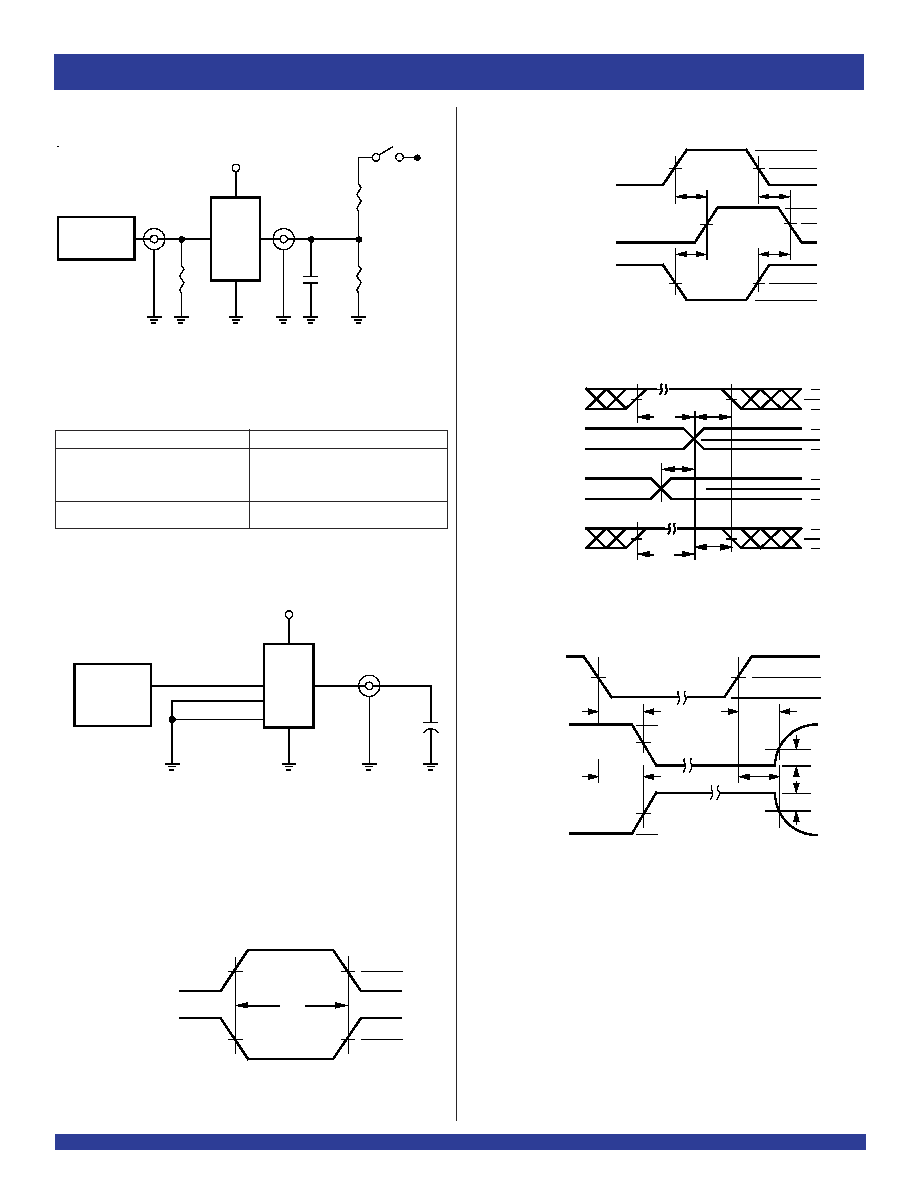
D.U.T.
V
CC
1 MHz
Signal
Generator
C
L
=
50pF
(3)
V
OUT
Switch
Out
Enable/Select
Switch In
Switch In (MUX)
(1)
(2)
Pulse
Generator
R
T
D.U.T.
V
CC
V
IN
C
L
V
OUT
50pF
500
500
7.0V
3V
1.5V
0V
3V
1.5V
0V
3V
1.5V
0V
3V
1.5V
0V
DATA
INPUT
TIMING
INPUT
ASYNCHRONOUS
CONTROL
SYNCHRONOUS
CONTROL
t
SU
t
H
t
REM
t
SU
t
H
HIGH-LOW-HIGH
PULSE
LOW-HIGH-LOW
PULSE
t
W
1.5V
1.5V
SAME PHASE
INPUT TRANSITION
3V
1.5V
0V
1.5V
V
OH
t
PLH
OUTPUT
OPPOSITE PHASE
INPUT TRANSITION
3V
1.5V
0V
t
PLH
t
PHL
t
PHL
V
OL
CONTROL
INPUT
3V
1.5V
0V
3.5V
0V
OUTPUT
NORMALLY
LOW
OUTPUT
NORMALLY
HIGH
SWITCH
CLOSED
SWITCH
OPEN
V
OL
0.3V
0.3V
t
PLZ
t
PZL
t
PZH
t
PHZ
3.5V
0V
1.5V
1.5V
ENABLE
DISABLE
V
OH
TEST CIRCUITS AND WAVEFORMS
Propagation Delay
Test Circuits for All Outputs
Enable and Disable Times
Set-up, Hold, and Release Times
Pulse Width
NOTES:
1. Diagram shown for input Control Enable-LOW and input Control Disable-HIGH.
2. Pulse Generator for All Pulses: Rate
1.0MHz; t
F
2.5ns; t
R
2.5ns.
Test
Switch
Open Drain
Disable Low
Closed
Enable Low
All Other Tests
Open
SWITCH POSITION
DEFINITIONS:
C
L
= Load capacitance: includes jig and probe capacitance.
R
T
= Termination resistance: should be equal to Z
OUT
of the Pulse Generator.
Charge Injection
NOTES:
1. Select is used with multiplexers for measuring IQ
DCI
I during multiplexer select. During
all other tests Enable is used.
2. Used with multiplexers to measure IQ
DCI
I only.
3. Charge Injection =
V
OUT
C
L
, with Enable toggling for IQ
CI
I or Select toggling for IQ
DCI
I.
V
OUT
is the change in V
OUT
and is measured with a 10M
probe.
6
INDUSTRIAL TEMPERATURE RANGE
IDT74FST1632861
20-BIT, TWO PORT BUS SWITCH WITH RESISTOR
ORDERING INFORMATION
CORPORATE HEADQUARTERS
for SALES:
for Tech Support:
2975 Stender Way
800-345-7015 or 408-727-6116
logichelp@idt.com
Santa Clara, CA 95054
fax: 408-492-8674
(408) 654-6459
www.idt.com
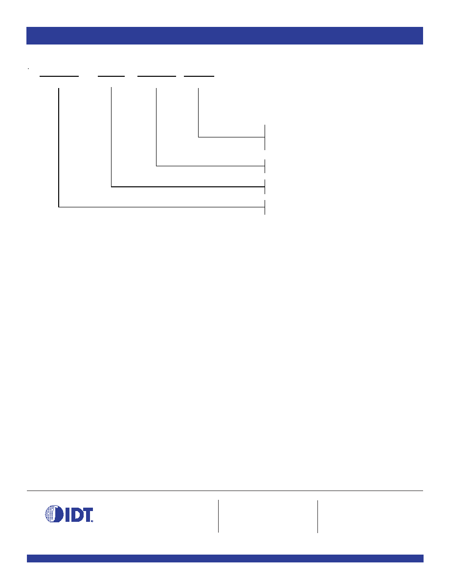
IDT XX
Temp. Range
XXX
Device Type
XX
Package
74
≠40∞C to +85∞C
PV
PA
PF
2861
Shrink Small Outline Package
Thin Shrink Small Outline Package
Thin Very Small Outline Package
20-Bit Flow Through Switch with Resistor
FST
XXX
Family
163
Double-Density Bus Switch