GTLP816.PMD
1
IDT74GTLP816
GTLP / TTL 1:2 / 1:6 CLOCK DRIVER
INDUSTRIAL TEMPERATURE RANGE
JUNE 2002
2002 Integrated Device Technology, Inc.
DSC-5965/9
c
IDT74GTLP816
PRELIMINARY
INDUSTRIAL TEMPERATURE RANGE
GTLP/TTL 1:2/1:6
CLOCK DRIVER
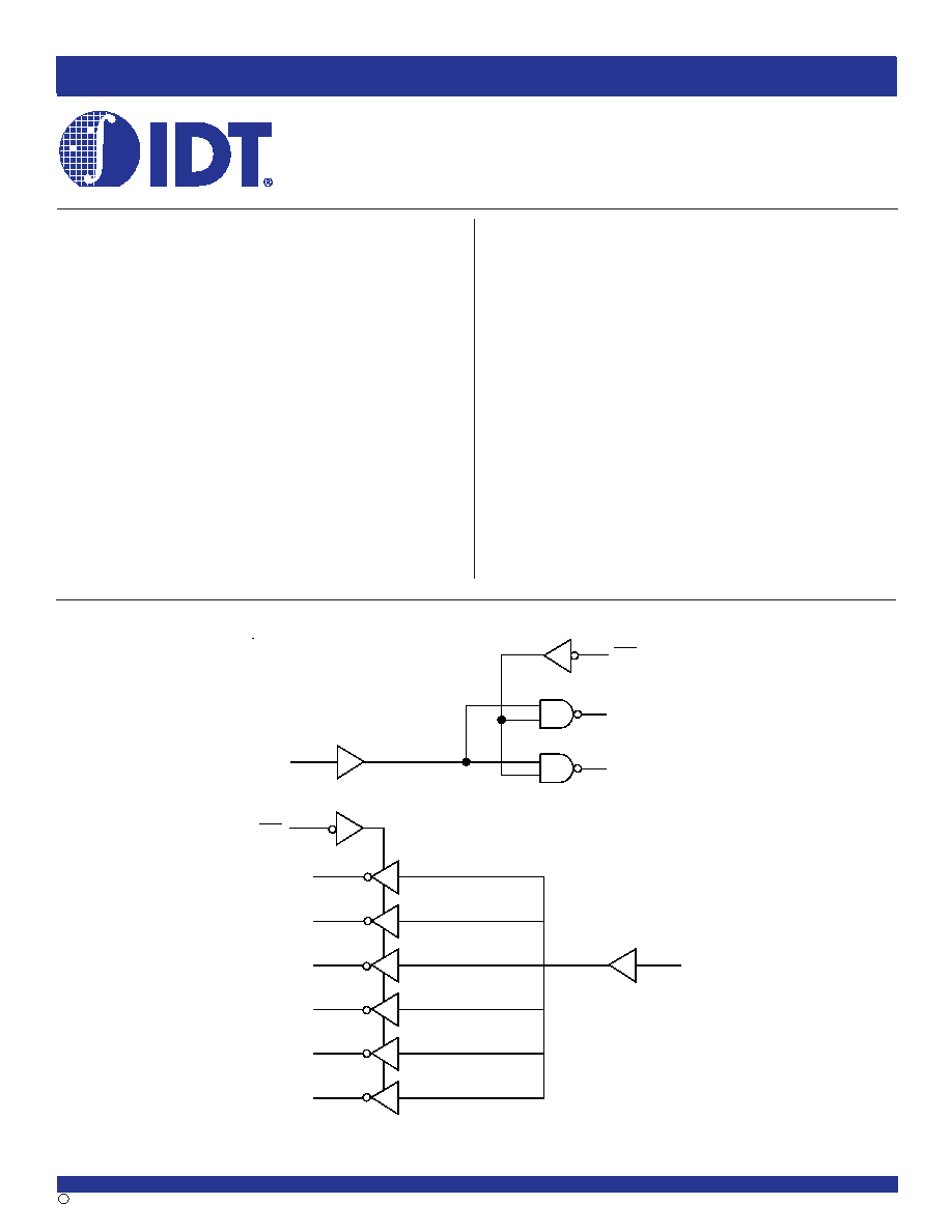
DESCRIPTION:
The GTLP816 is a GTLP to TTL (1:6) and TTL to GTLP (1:2) clock
driver with inverting outputs. The clock driver provides a high-speed
interface between cards operating at TTL logic levels and back-planes
operating at GTLP logic levels. GTLP provides reduced output swing
(<1V), reduced input threshold levels, and output edge-rate control to
minimize signal setting times. The GTLP816 is a derivative of the Gunning
Transceiver Logic (GTL) JEDEC standard JESD8-3 and incorporates
internal edge-rate control, which is process, voltage, and temperature
(PVT) compensated.
GTLP output low voltage is typically less than 0.5V. The output high is
1.5V, and the receiver threshold is 1V.
The GTLP816 is available in Industrial Temperature Range (-40�C to
+85�C). See Ordering Information for details.
OEA
OA
0
OA
1
OA
2
OA
3
OA
4
OA
5
GTLPIN
TTLIN
OB
0
OB
1
OEB
The IDT logo is a registered trademark of Integrated Device Technology, Inc.
FEATURES:
� Interface between GTLP and TTL logic levels
� GTLP to TTL 1:6 fanout
� TTL to GTLP 1:2 fanout
� Edge Rate Control Circuit reduces output noise on GTLP port
� V
REF
pin provides reference voltage for receiver threshold
� CMOS technology for low power dissipation
� Special PVT Compensation circuitry to provide consistent perfor-
mance over variations of process, supply voltage, and temperature
� 5V tolerant inputs and outputs on TTL ports
� TTL-compatible Driver and Control inputs
� High Output source/sink �24mA on TTL ports
� High Output sink +34mA on GTLP ports
� Open drain on GTLP to support wired-or connection
� Available in TSSOP package
FUNCTIONAL BLOCK DIAGRAM
2
INDUSTRIAL TEMPERATURE RANGE
IDT74GTLP816
GTLP / TTL 1:2 / 1:6 CLOCK DRIVER
TSSOP
TOP VIEW
PIN CONFIGURATION
TTLIN
GNDT
OA
1
GNDT
GND
T
OA
0
V
CCT
OA
2
OA
3
V
CCT
OA
4
OA
5
GNDT
GNDG
OB
0
OEA
OEB
V
REF
GNDG
OB
1
GNDG
GTLPIN
GNDT
V
CC
2
3
4
5
6
7
8
9
10
11
12
15
14
13
16
17
18
19
20
21
22
23
24
1
ABSOLUTE MAXIMUM RATINGS
(1,2)
Symbol
Rating
Max.
Unit
V
CC
Supply Voltage
�0.5 to +7
V
V
CCT
V
I
DC Input Voltage
�0.5 to +7
V
V
O
DC Output Voltage
3-State
�0.5 to +7
V
Active
�0.5 to V
CC
+ 0.5
I
OL
DC Output Sink Current into OA
64
mA
I
OH
DC Output Source Current from OA
�64
mA
I
OL
DC Output Sink Current into OB
80
mA
(in the LOW state)
I
IK
DC Input Diode Current
V
I
< 0V
�50
mA
I
OK
DC Output Diode Current V
O
< 0V
�50
mA
V
O
> V
CC
+50
T
STG
Storage Temperature
�65 to +150
�C
NOTES:
1. Stresses greater than those listed under ABSOLUTE MAXIMUM RATINGS may cause
permanent damage to the device. This is a stress rating only and functional operation
of the device at these or any other conditions above those indicated in the operational
sections of this specification is not implied. Exposure to absolute maximum rating
conditions for extended periods may affect reliability.
2. Unused inputs must be held HIGH or LOW.
CAPACITANCE
(T
A
= +25�C, f = 1.0MH
Z
)
Symbol
Parameter
(1)
Conditions
Typ.
(2)
Max. Unit
C
IN
Control Pins/GTLPIN/TTLIN V
I
= V
CC
or 0
3.7
--
pF
C
OUT
OAx
V
I
= V
CC
or 0
7
--
pF
OBx
V
I
= V
CC
or 0
7
--
pF
NOTES:
1. As applicable to the device type.
2. All typical values are at V
CC
, V
CCT
= 5V, T
A
= 25�C
PIN DESCRIPTION
Pin Names
Description
TTLIN, GTLPIN
Clock Inputs (TTL and GTLP)
OEB
Clock Enable for GTLP Outputs. Set LOW for normal operation.
OEA
Clock Enable for TTL Outputs. Set LOW for normal operation.
V
CCT
Power Supply for TTL Clock Outputs
GNDT
Ground for TTL Clock Outputs
V
CC
Power Supply for Internal Circuitry
GNDG
Ground for GTLP Clock Outputs
V
REF
Voltage Reference Input
OA
[5:0]
TTL Clock Outputs (Inverted)
OB
[1:0]
GTLP Clock Outputs (Inverted)
FUNCTION TABLE
(1)
Inputs
Outputs
(2)
OEB
OEA
GTLPIN
TTLIN
OAx
OBx
L
L
H
H
L
L
L
L
L
L
H
H
H
H
X
X
Z
Z
NOTES:
1. H = HIGH Voltage Level
L = LOW Voltage Level
X = Don't Care
Z = High Impedance
2. Output polarity is inverting.
3
IDT74GTLP816
GTLP / TTL 1:2 / 1:6 CLOCK DRIVER
INDUSTRIAL TEMPERATURE RANGE
RECOMMENDED OPERATING CONDITIONS
(1)
Symbol
Rating
Min.
Typ.
Max.
Unit
V
CC
,V
CCT
Supply Voltage
4.75
5
5.25
V
V
TT
Bus Termination Voltage
GTLP
1.47
1.53
V
V
REF
0.98
1.02
V
I
Input Voltage on TTLIN and Control Pins
0
--
5.5
V
I
OH
HIGH Level Output Current (OAx)
--
--
-24
mA
I
OL
LOW Level Output Current (OAx)
--
--
+24
mA
I
OL
LOW Level Output Current (OBx)
--
--
+34
mA
T
A
Operating Temperature
�40
+25
+85
�C
NOTE:
1. Unused inputs must be held HIGH or LOW.
NOTES:
1. All typical values are at V
CC
, V
CCT
= 5V, and T
A
= 25�C.
2.
I
CC
is the increase in supply current for each input that is at the specified TTL voltage level rather than V
CC
or GND.
DC ELECTRICAL CHARACTERISTICS OVER OPERATING RANGE
Following Conditions Apply Unless Otherwise Specified:
Industrial: T
A
= �40�C to +85�C; V
REF
= 1V; V
CC
,
V
CCT
= 5V � 5%
Symbol
Parameter
Test Conditions
Min.
Typ.
(1)
Max.
Unit
V
IH
GTLPIN
V
REF
+ 0.05
--
V
TT
V
All Others
2
--
--
V
IL
GTLPIN
0
--
V
REF
� 0.05
V
All Others
--
--
0.8
V
REF
GTLP
--
1
--
V
GTL
--
0.8
--
V
TT
GTLP
--
1.5
--
V
GTL
--
1.2
--
V
IK
V
CC
= Min, I
I
= �18mA
--
--
�1.2
V
I
OH
= �100�A
V
CC
�0.2
--
--
V
OH
OAx
V
CC
= Min
I
OH
= �18mA
2.4
--
--
V
I
OH
= �24mA
2.2
--
--
I
OL
= 100�A
--
--
0.2
V
OL
OAx
V
CC
= Min
I
OL
= 18mA
--
--
0.4
V
I
OL
= 24mA
--
--
0.5
V
OL
OBx
V
CC
= Min
I
OL
= 100�A
--
--
0.2
V
I
OL
= 34mA
--
--
0.65
I
I
TTLIN/Control Pins
V
CC
= Max
V
I
= 5.25V or 0V
--
--
�5
�A
GTLPIN
V
I
= V
TT
or 0V
--
--
�5
I
OFF
TTLIN
V
CC
= 0
V
I
or V
O
= 0 to 5.25V
--
--
100
�A
I
OZH
OAx
V
CC
= Max
V
O
= 5.25 V
--
--
5
�A
OBx
V
O
= 1.5V
--
--
5
I
OZL
OAx
V
CC
= Max
V
O
= 0
--
--
�5
�A
I
CC
OAx or OBx
V
CC
= Max
Outputs HIGH
--
7
18
Outputs LOW
--
7
20
mA
V
I
= V
CC
or GND
Outputs Disabled
--
7
20
I
CC
(2)
TTLIN
V
CC
= Max
V
I
= V
CC
- 2.1
--
--
6
mA
4
INDUSTRIAL TEMPERATURE RANGE
IDT74GTLP816
GTLP / TTL 1:2 / 1:6 CLOCK DRIVER
AC ELECTRICAL CHARACTERISTICS
(1,2)
Symbol
Parameter
Min.
Typ.
(3)
Max.
Unit
t
PLH
TTLIN to OBx
1.5
3.8
6
ns
t
PHL
1.5
2.8
5
t
PLH
OEB to OBx
1.5
6.4
10.5
ns
t
PHL
1.5
3.2
6
t
PLH
GTLPIN to OAx
1.5
4.4
6.5
ns
t
PHL
1.5
4
6
t
R
OBx Output Rise Time (20% to 80%)
--
2.3
--
ns
t
F
OBx Output Fall Time (20% to 80%)
--
2.3
--
t
R
OAx Output Rise Time (10% to 90%)
--
2
--
ns
t
F
OAx Output Fall Time (10% to 90%)
--
2
--
t
SK(o)
Output Skew
(4)
--
0.2
1
ns
t
PZH
OEA to OAx
0.5
3.6
6.5
ns
t
PZL
t
PHZ
0.5
3.8
6.5
ns
t
PLZ
NOTES:
1. See Test Circuits and Waveforms.
2. Unless otherwise noted, V
REF
= 1V, C
L
= 30pF for OBx, and C
L
= 50pF for OAx.
3. Typical values are at V
CC
, V
CCT
= 5V, and T
A
= 25�C.
4. Skew specs are given for specific, worst case V
CC
temp. Skew values between the OBx outputs could vary on the backplane due to loading and impedance seen by the
device.
5
IDT74GTLP816
GTLP / TTL 1:2 / 1:6 CLOCK DRIVER
INDUSTRIAL TEMPERATURE RANGE
6V
Open
GND
INPUT
0V
OUTPUT
V
OH
Vm
V
OL
OUTPUT
Vm
t
PHL
t
PLH
t
SK(O)
V
OH
V
OL
80%
20%
t
R,
t
F
INPUT
CONTROL
5V
0V
V
OH
V
OL
V
OL
V
OH �
0.3V
V
OH
V
OL +
0.3V
1.5V
OUTPUT
WAVEFORM 1
OUTPUT
WAVEFORM 2
t
PLZ
t
PZL
t
PZH
t
PHZ
1.5V
V
CC
/2
V
CC
/2
1.5V for TTL, 1V for GTLP, 0.8V for GTL
5V for TTL, 1.5V for GTLP, 1.2V for GTL
500
C
L
= 50pF
500
25
30pF
FROM
OUTPUT
UNDER
TEST
1.5V (GTLP)
1.2V (GTL)
FROM
OUTPUT
UNDER
TEST
S
(1)
(1)
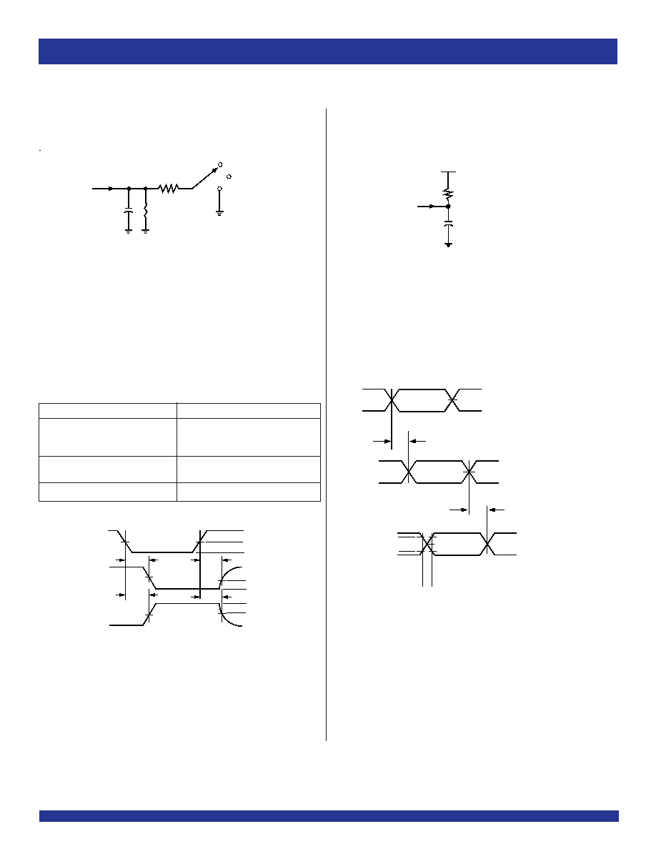
TEST CIRCUITS AND WAVEFORMS
Test Circuit for OA Outputs
NOTE:
1. C
L
includes probes and jig capacitance. C
L
= 30pF is used for worst case.
NOTE:
1. C
L
includes probes and jig capacitance.
NOTES:
Waveform 1 is for an output with internal conditions such that the output is LOW except when disabled by the output control.
Waveform 2 is for an output with internal conditions such that the output is HIGH except when disabled by the output control.
All input pulses have the following characteristics: frequency = 10 MHz, t
R
= t
F
= 2 ns, Z
O
= 50
. The outputs are measured one at a time with one transition per measurement.
Voltage Waveforms Pulse Duration
(Vm = V
CC
/2 for OAx and 1V for OBx )
Voltage Waveforms Enable and Disable Times (OAx)
SWITCH POSITION
Test
Switch
Open Drain
Disable Low
6V
Enable Low
Disable High
GND
Enable High
All Other Tests
Open
Test Circuit for OB Outputs