INDUSTRIAL TEMPERATURE RANGE
IDT74LVC161A
3.3V CMOS PRESETTABLE SYNCHRONOUS 4-BIT BINARY COUNTER
1
OCTOBER 1999
INDUSTRIAL TEMPERATURE RANGE
The IDT logo is a registered trademark of Integrated Device Technology, Inc.
©1999 Integrated Device Technology, Inc.
DSC-5156/1
FEATURES:
· 0.5 MICRON CMOS Technology
· ESD > 2000V per MIL-STD-883, Method 3015; > 200V using
machine model (C = 200pF, R = 0)
· V
CC
= 3.3V ± 0.3V, Normal Range
· V
CC
= 2.7V to 3.6V, Extended Range
· CMOS power levels (0.4
µµ
µµ
µ W typ. static)
· Rail-to-Rail output swing for increased noise margin
· All inputs, outputs, and I/Os are 5V tolerant
· Supports hot insertion
· Available in QSOP, SOIC, SSOP, and TSSOP packages
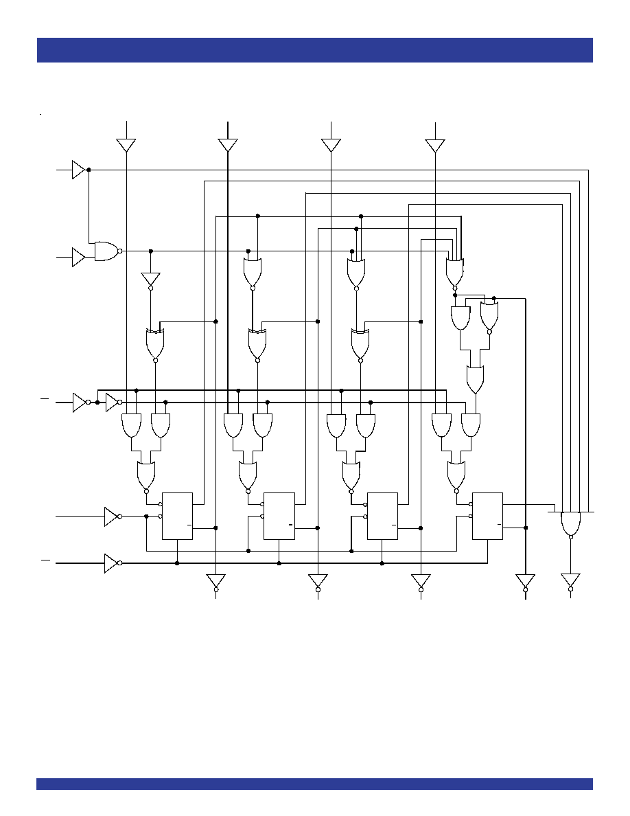
FUNCTIONAL DIAGRAM
DRIVE FEATURES:
· High Output Drivers: ±24mA
· Reduced system switching noise
APPLICATIONS:
· 5V and 3.3V mixed voltage systems
· Data communication and telecommunication systems
IDT74LVC161A
DESCRIPTION:
The LVC161A is a high-performance, low-power, low-voltage, Si-gate
CMOS device, superior to most advanced CMOS-compatible TTL families.
The LVC161A is a presettable synchronous binary counter which
3.3V CMOS PRESETTABLE
SYNCHRONOUS 4-BIT BINARY
COUNTER WITH ASYNCHRONOUS
RESET, 5 VOLT TOLERANT I/O
STATE DIAGRAM
Inputs can be driven from either 3.3V or 5V devices. This feature allows
the use of this device as a translator in a mixed 3.3V/5V supply system.
f
max
=
tp
(max)
(CP to TC) + t
su
(CEP to CP)
1
0
1
2
3
4
5
6
7
8
9
10
11
12
13
14
15
PARALLEL LOAD
CIRCUITRY
BINARY COUNTER
3
4
5
6
14
13
12
11
Q
0
Q
1
Q
2
Q
3
D
0
D
1
D
2
D
3
PE
CET
CEP
CP
MR
TC
9
10
7
2
1
15
features an internal look-ahead carry and can be used for high-speed
counting. Synchronous operation is provided by having all flip-flops clocked
simultaniously on the positive-going edge of the clock (CP). Outputs (Q
0
to
Q
3
) of the counters may be preset to a high or low level. A low level at the
parallel enable input (PE) disables the counting action and causes the data
at inputs (D
0
to D
3
) to be loaded into the counter on the positive-going edge
of the clock (provided that the set-up and hold time requirements for PE are
met). Preset takes place regardless of the levels at the count enable inputs
(CEP and CET). A low level at the master reset input (MR) sets all four outputs
of the flip-flops (Q
0
to Q
3
) to low level regardless of the levels at CP, PE, CET,
and CEP inputs (thus providing an asynchronous clear function).
The look-ahead carry simplifies serial cascading of the counters. Both
count enable inputs (CEP and CET) must be high to count. The CET input
is fed forward to enable the terminal count output (TC). The TC output thus
enabled will produce a high output pulse of a duration approximately equal
to a high level output of Q
0
. This pulse can be used to enable the next
cascaded stage. The maximum clock frequency for the cascaded counters
is determined by the CP to TC propagation delay and CEP to CP set-up time,
according to the following formula:
INDUSTRIAL TEMPERATURE RANGE
IDT74LVC161A
3.3V CMOS PRESETTABLE SYNCHRONOUS 4-BIT BINARY COUNTER
3
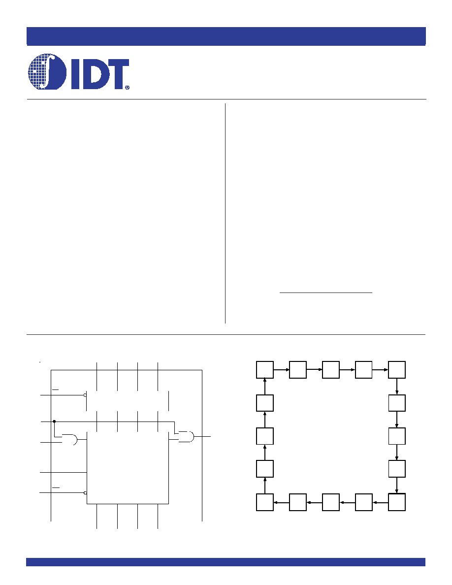
Pin Names
Description
MR
Asynchronous Master Reset (Active LOW)
C P
Clock Input (LOW-to-HIGH, Edge-Triggered)
Dx
Data Inputs
CEP
Count Enable Inputs
GND
Ground (0V)
PE
Parallel Enable Input (Active LOW)
CET
Count Enable Carry Input
Qx
Flip-Flop Outputs
TC
Terminal Count Output
Vcc
Positive Supply Voltage
PIN DESCRIPTION
QSOP/ SOIC/ SSOP/ TSSOP
TOP VIEW
D2
D3
MR
PE
D0
D1
CP
CEP
CET
Q0
Q1
Q2
Q3
TC
COUNT
INHIBIT
RESET PRESET
14
15
0
1
2
13
12
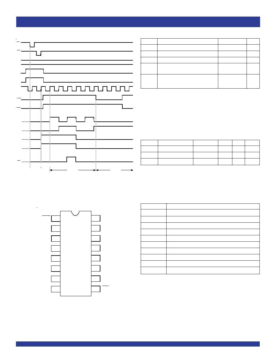
TYPICAL TIMING SEQUENCE
2
3
1
CP
V
CC
MR
5
6
4
CEP
7
10
CET
15
14
16
12
11
13
D
0
GND
8
9
PE
TC
D
1
D
2
D
3
Q
0
Q
1
Q
2
Q
3
PIN CONFIGURATION
NOTE:
1. As applicable to the device type.
Symbol
Parameter
(1)
Conditions
Typ.
Max.
Unit
C
IN
Input Capacitance
V
IN
= 0V
4.5
6
pF
C
OUT
Output Capacitance
V
OUT
= 0V
5.5
8
pF
C
I/O
I/O Port Capacitance
V
IN
= 0V
6.5
8
pF
CAPACITANCE
(T
A
= +25°C, F = 1.0MHz)
Symbol
Description
Max
Unit
V
TERM
Terminal Voltage with Respect to GND
0.5 to +6.5
V
T
STG
Storage Temperature
65 to +150
°C
I
OUT
DC Output Current
50 to +50
mA
I
IK
Continuous Clamp Current,
50
mA
I
OK
V
I
< 0 or V
O
< 0
I
CC
Continuous Current through each
±100
mA
I
SS
V
CC
or GND
ABSOLUTE MAXIMUM RATINGS
(1)
NOTE:
1. Stresses greater than those listed under ABSOLUTE MAXIMUM RATINGS may cause
permanent damage to the device. This is a stress rating only and functional operation
of the device at these or any other conditions above those indicated in the operational
sections of this specification is not implied. Exposure to absolute maximum rating
conditions for extended periods may affect reliability.
INDUSTRIAL TEMPERATURE RANGE
4
IDT74LVC161A
3.3V CMOS PRESETTABLE SYNCHRONOUS 4-BIT BINARY COUNTER
Symbol
Parameter
Test Conditions
Min.
Typ.
(1)
Max.
Unit
V
IH(2)
Input HIGH Voltage Level
V
CC
= 2.3V to 2.7V
1.7
--
--
V
V
CC
= 2.7V to 3.6V
2
--
--
V
IL
Input LOW Voltage Level
V
CC
= 2.3V to 2.7V
--
--
0.7
V
V
CC
= 2.7V to 3.6V
--
--
0.8
I
IH
Input Leakage Current
V
CC
= 3.6V
V
I
= 0 to 5.5V
--
--
±5
µA
I
IL
I
OZH
High Impedance Output Current
V
CC
= 3.6V
V
O
= 0 to 5.5V
--
--
±10
µA
I
OZL
(3-State Output pins)
I
OFF
Input/Output Power Off Leakage
V
CC
= 0V, V
IN
or V
O
5.5V
--
--
±50
µA
V
IK
Clamp Diode Voltage
V
CC
= 2.3V, I
IN
= 18mA
--
0.7
1.2
V
V
H
Input Hysteresis
V
CC
= 3.3V
--
100
--
mV
I
CCL
Quiescent Power Supply Current
V
CC
= 3.6V, V
IN
= GND or V
CC
--
--
10
µA
I
CCH
I
CCZ
I
CC
Quiescent Power Supply Current
One input at V
CC
- 0.6V, other inputs at V
CC
or GND
--
--
500
µA
Variation
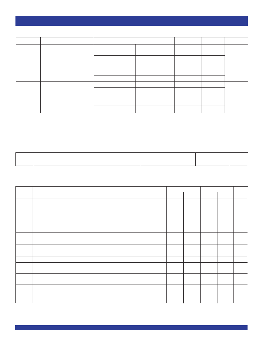
DC ELECTRICAL CHARACTERISTICS OVER OPERATING RANGE
Following Conditions Apply Unless Otherwise Specified:
Operating Condition: T
A
= 40°C to +85°C
NOTES:
1. Typical values are at V
CC
= 3.3V, +25°C ambient.
2. Clock Pin (CP) requires a minimum V
IH
of 2.5V.
FUNCTION TABLE
(1)
OPERATING
INPUTS
OUTPUTS
MODES
MR
CP
CEP
CET
PE
Dx
Qx
TC
Reset (clear)
L
X
X
X
X
X
L
L
Parallel load
H
X
X
l
l
L
L
H
X
X
l
h
H
*
Count
H
h
h
h
X
count
*
Hold
H
X
l
X
h
X
Q
(2)
*
(do nothing)
H
X
X
l
h
X
Q
(2)
L
NOTE:
1. H = HIGH Voltage Level
h = HIGH Voltage level one setup time prior to the LOW-to-HIGH clock transition.
L = LOW Voltage Level
l = LOW Voltage level one setup time prior to the LOW-to-HIGH clock transition.
X = Don't care
* = The TC output is HIGH when CET is HIGH and the counter is at Terminal Count (HHHH).
= LOW-to-HIGH clock transition
2. Indicates the state of the referenced output one set up time prior to the LOW-to-HIGH clock transition.
INDUSTRIAL TEMPERATURE RANGE
IDT74LVC161A
3.3V CMOS PRESETTABLE SYNCHRONOUS 4-BIT BINARY COUNTER
5
SWITCHING CHARACTERISTICS
(1)
V
CC
= 2.7V
V
CC
= 3.3V ± 0.3V
Symbol
Parameter
Min.
Max.
Min.
Max.
Unit
t
PLH
Propagation Delay
--
9
--
8
ns
t
PHL
CP to Qx
t
PLH
Propagation Delay
--
11
--
9.5
ns
t
PHL
CP to TC
t
PLH
Propagation Delay
--
8.8
--
7.8
ns
t
PHL
CET to TC
t
PLH
Propagation Delay
--
10
--
9
ns
MR to Qx
t
PHL
Propagation Delay
--
11
--
10
ns
MR to TC
t
W
Clock Pulse Width, HIGH or LOW
5
--
4
--
ns
t
W
Master Reset Width LOW
4
--
3
--
ns
t
REM
Removal Time, MR to CP
0.5
--
0.5
--
ns
t
SU
Set-Up Time, Dx to CP
3.5
--
3
--
ns
t
SU
Set-Up Time, PE to CP
3.5
--
3
--
ns
t
SU
Set-Up Time, CEP, CET to CP
5.5
--
5
--
ns
t
H
Hold Time, Dx, PE, CEP, CET to CP
0
--
0
--
ns
t
SK
(o)
Output Skew
(2)
--
--
--
500
ps
NOTES:
1. See TEST CIRCUITS AND WAVEFORMS. T
A
= 40°C to + 85°C.
2
Skew between any two outputs of the same package and switching in the same direction.
OPERATING CHARACTERISTICS, V
CC
= 3.3V ± 0.3V, T
A
= 25°C
Symbol
Parameter
Test Conditions
Typical
Unit
C
PD
Power Dissipation Capacitance
C
L
= 0pF, f = 10Mhz
--
pF
NOTE:
1. V
IH
and V
IL
must be within the min. or max. range shown in the DC ELECTRICAL CHARACTERISTICS OVER OPERATING RANGE table for the appropriate V
CC
range.
T
A
= 40°C to + 85°C.
OUTPUT DRIVE CHARACTERISTICS
Symbol
Parameter
Test Conditions
(1)
Min.
Max.
Unit
V
OH
Output HIGH Voltage
V
CC
= 2.3V to 3.6V
I
OH
= 0.1mA
V
CC
0.2
--
V
V
CC
= 2.3V
I
OH
= 6mA
2
--
V
CC
= 2.3V
I
OH
= 12mA
1.7
--
V
CC
= 2.7V
2.2
--
V
CC
= 3V
2.4
--
V
CC
= 3V
I
OH
= 24mA
2.2
--
V
OL
Output LOW Voltage
V
CC
= 2.3V to 3.6V
I
OL
= 0.1mA
--
0.2
V
V
CC
= 2.3V
I
OL
= 6mA
--
0.4
I
OL
= 12mA
--
0.7
V
CC
= 2.7V
I
OL
= 12mA
--
0.4
V
CC
= 3V
I
OL
= 24mA
--
0.55