 | –≠–ª–µ–∫—Ç—Ä–æ–Ω–Ω—ã–π –∫–æ–º–ø–æ–Ω–µ–Ω—Ç: 75T43100 | –°–∫–∞—á–∞—Ç—å:  PDF PDF  ZIP ZIP |
JULY 2001
DSC-5325/01
1
2002 Integrated Device Technology, Inc.
All rights reserved. Product specifications subject to change without notice.
©
Features
x
x
x
x
x
32K x72 bit Data Cells and 32K x72 bit Mask Cells
x
x
x
x
x
Full ternary content addressable memory
x
x
x
x
x
36/72/144/288 multiple width lookups
x
x
x
x
x
66M sustained lookups per second at 72 and 144 width lookups
x
x
x
x
x
Commercial and Industrial Speed Grades
x
x
x
x
x
Synchronous pipeline operation
x
x
x
x
x
Dual bus interface
x
x
x
x
x
Cascadable to 8 devices with no glue logic or latency penalty
x
x
x
x
x
Glueless interface to standard ZBTTM or
Synchronous Pipelined Burst SRAMs
x
x
x
x
x
Boundary Scan JTAG Interface (IEEE 1149.1 compliant)
x
x
x
x
x
2.5V core power supply
x
x
x
x
x
User selectable 3.3V or 2.5V I/O supply
x
x
x
x
x
1.5V match supply
x
x
x
x
x
Packaged in a JEDEC standard, thermally enhanced,
low profile 304 Ball Grid Array (BGA)
IP Co-PROCESSOR
32K Entries
Preliminary
Information
IDT75T43100
The IDT75T43100 is designed to be used in applications that require
high speed data searching such as routers, high layer switching and
applications involved in the convergence of voice, data and video.
IDT's IP Co-Processors (IPCs) expedite multi level routing of IP
(Internet Protocol) and includes on chip logic to facilitate various types of
IP header lookups and processing of the results.
The features of this device address the performance requirements of
communication systems, which can require a sustained bandwidth of tens
of millions of lookups per second. IDT's IP Co-Processor is designed to
provide a scalable solution to one of the major bottlenecks facing the
bandwidth challenge of Internet traffic.
Overview
IDT's 75T43100 is a high performance pipelined, synchronous 32K
x72 IP Co-Processor (IPC). It utilizes content addressable memory
(CAM) technology to perform pattern recognition functions. Each location
in the IPC has both a Data entry and an associated Mask entry with the
total array size of 32K x72 Data entries and 32K x72 Mask entries.
The IDT75T43100 has a 72-bit bi-directional bus, which is a 15-bit
multiplexed address and 72-bit data bus that can support 66 million
sustained searches per second.
This device was developed for a wide range of communication and
networking applications, giving it the ability to support the requirements of
multiple networks. IPC's are used in applications that require high speed
data searching routers, high layer switching and in the convergence of
voice, data, and video. IDT's IPC increases the throughput for the
demanding networking and Internet systems.
The IDT75T43100 utilizes IDT's latest high-performance 0.18 u
CMOS processing technology and is packaged in a JEDEC Standard,
thermally enhanced, low profile, 304 Ball Grid Array (BGA).
Abstract
5 3 2 5 d 0 0
75T43100
S66BS
2
IDT75T43100
Preliminary Information
IP Co-Processor 32K Entries Commercial and Industrial Temperature Ranges
Block Diagram
Configuration Registers
and
Ram Control Circuits
CLK2X
˜
CCLK
˜ 2
RDACK
VALID
CONFIGIN
MATCHIN [6:0]
WE
HITACK
P
R
I
O
R
I
T
Y
E
N
C
O
D
E
R
S
I
Z
E
L
O
G
I
C
Search Result Registers
DATA
[71:0]
D
E
C
O
D
E
Address
A0 - A14
G M R
a n d
S R R
D e c o d e
I N S T
D e c o d e
MATCHOUT
INDX
[19:0]
REQDATA
REQSTB
R/W
5325 drw 01
RST
CMD [3:0]
CMD [6:4]
Command
Bus
PHASEN
JTAG
TMS
TDI
TCK
TRST
CE
/
OE
Global Mask Registers
[71:0]
TDO
Request
Bus
Index
Bus
CONFIGOUT
32K X 72
Bypass
6.42
3
IDT75T43100 Preliminary Information
IP Co-Processor 32K Entries Commercial and Industrial Temperature Ranges
x
x
x
x
x
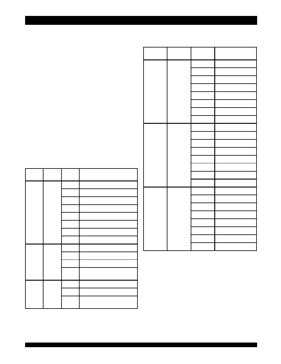
System Configurations and Functional Highlights
x
x
x
x
x
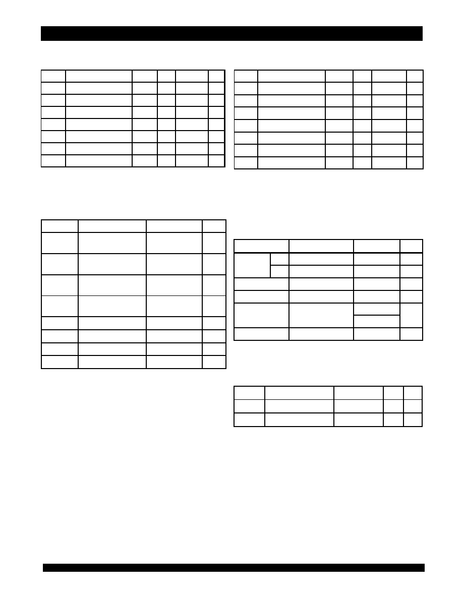
Signal Descriptions and Pinout
x
x
x
x
x
DC Operating Characteristics
x
x
x
x
x
Register Description
-
Configuration Registers
-
Reply Width Registers (RWRs)
-
Search Result Registers (SRRs)
-
Global Mask Registers (GMRs)
x
x
x
x
x
Bus Description
-
Command Bus Format
-
GMR and SRR Select
-
Request Bus Format
-
Index Bus Format
-
Additional Signals
x
x
x
x
x
Initialization
x
x
x
x
x
AC Operating Characteristics
x
x
x
x
x
Timing Diagrams
x
x
x
x
x
Sequence Diagrams
x
x
x
x
x
JTAG Interface Specifications
x
x
x
x
x
Package Diagram Outline
x
x
x
x
x
Ordering Information
Functional Highlights
System Configurations and Functional Highlights
Figure 1.1
System Configurations
Figure 1.0A ASIC / IP Co-Processor / SRAM configuration
Figure 1.0B - ASIC / IP Co-Processor configuration
Bus Interface
The IP Co-Processor utilizes a dual bus interface consisting of the
Request Bus and the Index Bus.
The 72 bit bi-directional Request Bus functions as a multiplexed address
and data bus, which performs the writing and reading of IP Co-Processor
resources, as well as presenting lookup data to the device.
The Index Bus is an independent unidirectional bus which drives the
result of the lookup (or index) to either an SRAM device or an ASIC. In
addition to driving the Index, the IPC also drives the associated SRAM
control signals (
CE/OE, and WE) for either ZBTTM or Synchronous
Pipeline Burst SRAM devices.
Reading data, mask or register entries will always result in 72 bits of data
driven on the Request Bus. Writes will also be 72 bits of data.
Data and Mask Array
The IDT75T43100 has 32K x 72 Data cell
entries and 32K x 72 associated Mask cell
entries as shown in Fig. 1.1. This combination
of Data and Mask cell entries enables the
IDT75T43100 to store 0, 1 or X, making it a full
ternary array IP Co-Processor. During a
lookup operation, both arrays are used along
with a Global Mask Register to find a match to
a requested data word.
The IDT75T43100 is designed to fulfill the needs of various types of
Networking systems. In solutions requiring data searching such as
routers, a network interface as shown in Fig 1.0A may be realized. Here
the IDT IP Co-Processor (IPC) interfaces directly to an ASIC/ FPGA for
lookups and routes an index to an associated SRAM device, that supplies
the next hop address via an SRAM Data Bus to the ASIC. The IPC also
provides the required control signals to directly hookup to ZBTTM
or
Synchronous Pipeline Burst SRAM.
IDT's IPC can also be configured without using the SRAM interface
as shown in Fig. 1.0B Here the IDT75T43100 processes the lookups
submitted by the controller and feeds the result directly back to the ASIC/
FPGA. In this manner, the full capabilities of the IPC are fully utilized without
requiring the use of an external SRAM.
The IPC provides the user control of the associated handshake
signals to adapt to either configuration.
Command Bus
The IDT75T43100 carries a 7-bit Command Bus, which loads specific
instructions into the IP Co-Processor. These include:
x
Read or Write
A Read or Write instruction placed on the Command Bus operates on
a specified data entry, mask entry, or register. During the initiation of a
Read command, the Request Bus will be driven with an address, a fixed
number of clock cycles later this same bus will be driven with the respective
data back . During the initiation of a Write command, the Request Bus will
receive the address during the 1st cycle followed by the respective data
on the 2nd cycle. All reads and writes are 72-bit entities.
Datasheet Features
A5325 drw 03
32K x 72
D a ta
Mask
A5325 drw02a
ASIC
or
FPGA
Network Interface
IDT
IP Co-Processor
Sync
or
ZBT SRAM
A 5 325 drw 0 2b
Network Interface
ASIC
or
FPGA
IDT
IP Co-Processor

4
IDT75T43100
Preliminary Information
IP Co-Processor 32K Entries Commercial and Industrial Temperature Ranges
Functional Highlights continued
Functional Highlights
SRAM Interface
The IDT75T43100 provides all required address and control signals
for a glueless SRAM interface. When the user reads from or writes to the
external SRAM, the IPC provides a pipelined bypass path that takes the
20-bit Address off the Request Bus and drives them to the Index Bus. Refer
to the Request Bus Format and the Index Bus Format for more information.
The ASIC/FPGA handles the pipelining of the data to and from the SRAM.
Control signal timing is programmed to accommodate standard ZBT
SRAMs, as well as Synchronous Pipelined Burst SRAMs. More detailed
information, along with how to configure this interface is discussed in the
"Initialization" section.
Registers
The IDT75T43100 utilizes 31 registers to provide additional features
and convenience. There are four basic types of registers supported:
- 4 Configuration Registers
- 4 Reply width Registers (RWRs)
- 8 Search Result Registers (SRRs)
- 15 Global Mask Registers (GMRs)
GMRs are provided to support Lookup instructions to mask individual
bits during a search. Initialization of the IPC uses the Configuration
Registers to define the timing of outputs and the SRAM interface configu-
ration. The Configuration registers are also used to specify certain
parameters when the IDT75T43100 is used in a multiple IPC implemen-
tation.
Further details of each type of register and their specific implementation
are discussed in the sections titled under their respective register type. Also
refer to the "Command Bus Format, GMR and SRR Select" and
"Initialization" sections for addressing and setup of these registers.
Width Capability
The IDT75T43100 is capable of performing lookups or comparisons
on data structures of 72 bits, 144 bits and 288 bits. The internal memory
bank of the device can be used in three standard width arrays, as shown
in Figure 1.2.
x
- 32K x72
x
- 16K x144
x
- 8K x288
Figure 1.2
The IDT75T43100 can also provide the address and control signals
for a read or write to an associated SRAM memory. The IPC pipelines
the address from the Request Bus to the Index Bus, driving it out to the
associated SRAM. The ASIC/FPGA handles the pipelining of the data to
and from the SRAM.
x
SRAM No Wait Read
An SRAM No Wait Read is a Read instruction to an external SRAM
that can be pipelined within a series of operations. A standard Read
instruction to an external SRAM requires the read to complete prior to
submitting the next instruction. However, the SRAM No Wait Read
instruction does not require the user to wait for a Read to complete. The
next instruction can be loaded sequentially on the following cycle.
x
Lookup
A lookup can be requested in 72-bit, 144-bit or 288-bit widths. A 36-bit
lookup can be accomplished by using GMRs 10 and 11, refer to the
application note (AN-270), "Implementing x36-bit Lookups". The Com-
mand Bus identifies the specific registers to be used with a particular lookup.
All the instructions and associated commands are described in the
"Command Bus Format" and "GMR and SRR Select" sections. Please
refer to these sections for further definition of the instruction code.
16K X 144
32K X 72
32K X 72
4K X 288
8K X 288
A5325 drw 03a

6.42
5
IDT75T43100 Preliminary Information
IP Co-Processor 32K Entries Commercial and Industrial Temperature Ranges
Signal Descriptions
Signal Descriptions and Pinout
Symbol
Pin Function
# Pins
I/O
Description
IPC Buses:
CMD
Command
Bus
7
Input
The Command Bus defines the operation to be performed by the IPC. It also specifies the
lookup type and Global Mask Register to select. It is qualified by the Request Strobe signal to
define a valid IPC operation.
REQDATA
Request Bus
72
Input/Output
Three State
The Request Bus is a multiplexed address/data bus used to perfo rm reads (and writes) from
(to) the IPC, and to present search data for lookups.
INDX
Index Bus
20
Output
Three State
This b us is used to d rive the add ress of an external SRAM, o r fe ed bac k Lo okup result
information directly to the IPC's controller. Bits [14:0] of the Index Bus contain the encoded
location at which the compare was found.
REQSTB
Request Strobe
1
Input
This input signifies a valid input request. It is an active high signal that indicates the start of an
IPC operation cycle, it must b e active for two CLK2X cycles.
IPC and SRAM Control:
RDACK
Read
Acknowledge
1
Output
This is an active high signal that is sent back with data being read from the IPC on the Request
Data Bus, or with data being read from the associated external SRAM. In the case of SRAM
Read, RDACK is sent with the Index, or up to six cycles after the Index as d efined by the
Pipeline Delay (PD) field. In a depth expanded configuration, o nly the last (lowest priority) IPC
device in the IPC system must have the LC bit set and will drive the RDACK signal. Refer to
System Configuration Register for details on the PD and LC bits.
HITACK
Match
Acknowledge
1
Output
This is an active high signal that is sent with the Index, or up to six CLK2X cycles after the Index
as defined by the Pipeline Delay (PD) field. In a depth expanded configuration, only the last
(lowest priority) IPC device in the IPC system must have the LC bit set and will drive the HITACK
signal. This signal will be driven low if there was no match, high if a match was found. Refer
to System Configuration Register for details on the PD and the LC bits.
VALID
Valid
Lookup Bit
1
Output
This is an active high signal that is sent with the Index, or up to six CLK2X cycles after the Index
as defined by the Pipeline Delay (PD) field. In a depth expanded configuration, only the last
(lo west priority) IPC device in the IPC syste m must have the LC bit set and will drive the VALID
signal. It will be driven high upon the completion of a lookup, even if the lookup did not result
in a hit. Refer to System Configuration Register for details on the PD and LC bits.
CE / OE
Chip Enable/
Output Enable
1
Output
Three State
This is an active low output signal that is driven along with the Index Bus. It is connected to the
CE input pin of a ZBT SRAM or to the OE pin of a PBSRAM. In a depth expanded configuration,
only the last (lowest priority) IPC device in the IPC group must have the LS bit set and will drive
the
CE/OE signal. Refer to System Configuration Register for details on the LS bit.
WE
Write Enable
1
Output
Three State
This is an active low output signal which is driven along with the Index bus. It may be used to
assert the
WE pin of an external SRAM. In a depth expanded configuration, only the last (lowest
priority) IPC device in the IPC group must have the LS bit set and will drive the
WE signal.
Refer to System Configuration Register for de tails on the LS bit.
Clock and Initialization:
CLK2X
Clock Input
1
Input
All inputs and outputs are referenced to the positive edge of this clock.
PHASEN
Clock Phase
Enable
1
Input
This signal is used to generate an internal clock (CCLK) at Ω the frequency of CLK2X. When
PHASEN drives low, the CCLK clock is aligned with the rising e dge of CLK2X and insures that
a requeste d command gets properly registered into the device. An external clock (similar to
CCLK) maybe optionally generated by the use r to clock the external synchronous SRAM.
CONFIGIN
Configuration
Address
1
Input
This pin is used to set the Device ID internally at power up and whenever the
RST pin is held
low. In a depth expanded configuration, only the first device in the IPC system needs to be
set high.
CONFIGOUT
Configuration
Address
1
Ouput
This pin is used at power up and when RST is active to set the Device ID. In a depth expanded
co nfig uration, the CONFIGOUT signal is co nne cted to the CONFIGIN signal of the next
subsequent downstream IPC device.
RST
Reset
1
Input
This pin must be active (low) during power up. This will force all outputs to a high impedence
co ndition, as well as clearing the IPC enable (EN) b it in the System Configuration Register. This
function does not initialize the contents of the IPC entries.
B5325 tbl 01
6
IDT75T43100
Preliminary Information
IP Co-Processor 32K Entries Commercial and Industrial Temperature Ranges
Signal Descriptions continued
Symbol
Pin Function
# Pins
I/O
Description
Depth Expansion:
MATCHOUT
Match
Output
1
Output
Match Output is an active high signal that is driven one cycle before the Index is driven on the
bus. This signal signifies that a match has occurred in the IPC. The Match Output signal is active
high and is fed into a Match Input line of all lower priority IPC(s).The Match Output signal is
reference to 2.5V operating characteristic, regardless of selected V
DDQ
.
MATCHIN
Match
Input
7
Input
The Match Input signal is driven by all upstream Match Output signals. This indicates to all down
stream IPCs that a hit in a higher priority IPC has occurred. This will prevent a lower priority IPC
from driving the Index bus if a higher priority IPC encountered a match.
JTAG Signals:
TMS
Test Mode
Select
1
Input
JTAG instruction input. This is 1149 compliant and has Input levels the same as the other input
pins of the device. If set at 2.5V or 3.3V V
DDQ
This pin has an internal pullup
TDI
Test Data Input
1
Input
JTAG data input. This pin has an internal pullup
TDO
Test Data
Output
1
Output
Tristate
JTAG Data output pin. This pin is driven on the high to low edge of Test Clock.
TCK
Test Clock
1
Input
A maximum of 10Mhz test clock. This pin has an internal pullup
TRST
JTAG Reset
1
Input
Asynchronous JTAG Reset. This is an active low signal that will reset only JTAG associated
logic. This will have no affect on the other IPC functional logic. This pin has an internal pullup
Power Supply:
V
DD
Core Power
29
Supply
2.5V core power supply pins for the device
V
DDQ
I/O Power
26
Supply
2.5V or 3.3V I/O supply voltages for the device
V
MATCH
Match Power
46
Supply
1.5V match supply voltage for the device
V
DDQ
Select
I/O Power
1
Input
This is a DC signal that defines the output drive to be either 3.3V or 2.5V. To select 3.3V output
drive set V
DDQ
Select Low (Vss), for 2.5V output drive set V
DDQ
Select High (V
DDQ
).
Vss
Ground
69
Supply
Common gro und pins for IPC supply voltages
Other:
DNU
Do Not Use
9
N/A
Do not connect these pins
NC
No Connect
1
N/A
This p in is not conne cted to the d ie, can be left floating or connected to Vss to minimize thermal
impedance
B5325 tbl 01a
Signal Descriptions and Pinout

6.42
7
IDT75T43100 Preliminary Information
IP Co-Processor 32K Entries Commercial and Industrial Temperature Ranges
Pin Configuration -304 Ball Grid Array
Signal Descriptions and Pinout
1
2
3
4
5
6
7
8
9
10
11
12
13
14
15
16
17
18
19
20
21
22
23
A
VSS VSS VSS
REQ
DATA
18
VDD
VDDQ
VSS VDD VSS VSS VSS
REQ
DATA
0
VSS
V
MATCH
V
MATCH
V
MATCH
VSS
V
MATCH
VDD
TRST
VSS VSS VSS
A
B
VSS VSS VSS
REQ
DATA
19
REQ
DATA
16
REQ
DATA
14
V
MATCH
VDDQ
VSS
VDDQ
REQ
DATA
3
REQ
DATA
1
VSS
V
MATCH
V
MATCH
V
MATCH
VSS
V
MATCH
DNU
TDI VSS VSS VSS
B
C
VSS VSS
REQ
DATA
21
VDD
REQ
DATA
17
REQ
DATA
15
REQ
DATA
12
REQ
DATA
10
REQ
DATA
8
REQ
DATA
6
REQ
DATA
4
VDDQ
VSS
V
MATCH
V
MATCH
V
MATCH
VSS
V
MATCH
VSS VDD TMS VSS VSS
C
D
REQ
DATA
24
REQ
DATA
23
VDDQ
REQ
DATA
20
VDDQ V
MATCH
REQ
DATA
13
REQ
DATA
11
REQ
DATA
9
REQ
DATA
7
REQ
DATA
5
REQ
DATA
2
VSS
V
MATCH
VDDQ
SELE CT
V
MATCH
VSS
V
MATCH
TCLK
TDO NC
CONFIG
IN
RD-
ACK
D
E
REQ
DATA
26
REQ
DATA
25
VDD
REQ
DATA
22
75T43100
304-BGA
RST VDD
HIT
ACK
VALID
E
F
REQ
DATA
28
VDD
REQ
DATA
27
VDDQ
VDDQ
WE VDD
CE/
OE
F
G
REQ
DATA
31
REQ
DATA
30
VDDQ
REQ
DATA
29
CONFIG
OUT
VDDQ
DNU DNU
G
H
VSS
V
MATCH
V
MATCH
V
MATCH
V
MATCH
V
MATCH
V
MATCH
VSS
H
J
VDDQ
REQ
DATA
33
REQ
DATA
32
VDD
VDD
DNU DNU
VDDQ
J
K
REQ-
STB
VDD
REQ
DATA
35
REQ
DATA
34
INDX
19
INDX
18
VDD
INDX
17
K
L
CMD
4
CMD
5
CMD
6
VSS
VSS
INDX
16
VDDQ
INDX
15
L
M
VSS VDD
CMD
2
CLK-
2X
VDD
MATCH
OUT
INDX
14
VSS
M
N
PHA-
SEN
CMD
3
CMD
1
VSS
VSS
INDX
13
VDDQ
DNU
N
P
CMD
0
VDD
REQ
DATA
36
REQ
DATA
37
INDX
10
INDX
11
VDD
INDX
12
P
R
VDDQ
REQ
DATA
38
REQ
DATA
39
VDD
VDD
INDX
8
INDX
9
VDDQ
R
T
VSS
V
MATCH
V
MATCH
V
MATCH
V
MATCH
V
MATCH
V
MATCH
VSS
T
U
REQ
DATA
40
REQ
DATA
41
VDDQ
REQ
DATA
42
INDX
5
VDDQ
INDX
6
INDX
7
U
V
REQ
DATA
43
VDD
REQ
DATA
44
VDDQ
VDDQ
INDX
3
VDD
INDX
4
V
W
REQ
DATA
45
REQ
DATA
46
VDD
REQ
DATA
49
MATCH
IN
5
VDD
INDX
1
INDX
2
W
Y
REQ
DATA
47
REQ
DATA
48
VDDQ
REQ
DATA
51
VDDQ V
MATCH
REQ
DATA
58
REQ
DATA
60
REQ
DATA
62
REQ
DATA
64
REQ
DATA
66
REQ
DATA
69
VSS
V
MATCH
VDD
V
MATCH
VSS
V
MATCH
DNU
MATCH
IN
2
MATCH
IN
4
MATCH
IN
6
INDX
0
Y
AA
VSS VSS
REQ
DATA
50
VDD
REQ
DATA
54
REQ
DATA
56
REQ
DATA
59
REQ
DATA
61
REQ
DATA
63
REQ
DATA
65
REQ
DATA
67
VDDQ
VSS
V
MATCH
V
MATCH
V
MATCH
VSS
V
MATCH
DNU
VDD
MATCH
IN
3
VSS VSS
AA
AB
VSS VSS VSS
REQ
DATA
52
REQ
DATA
55
REQ
DATA
57
V
MATCH
VDDQ
VSS
VDDQ
REQ
DATA
68
REQ
DATA
70
VSS
V
MATCH
V
MATCH
V
MATCH
VSS
V
MATCH
DNU
MATCH
IN
1
VSS VSS VSS
AB
AC
VSS VSS VSS
REQ
DATA
53
VDD
VDDQ
VSS VDD VSS VSS VSS
REQ
DATA
71
VSS
V
MATCH
V
MATCH
V
MATCH
VSS
V
MATCH
VDD
MATCH
IN
0
VSS VSS VSS
AC
1
2
3
4
5
6
7
8
9
10
11
12
13
14
15
16
17
18
19
20
21
22
23
B5325 tbl 02A
8
IDT75T43100
Preliminary Information
IP Co-Processor 32K Entries Commercial and Industrial Temperature Ranges
Recommended Operating
Temperature and Supply Voltage
Recommended DC Operating
Conditions with V
DDQ
at 2.5V
NOTES:
1. V
IL
(min.) = ≠1.0V for pulse width less than t
CYC
/2, once per cycle.
2. V
IH
(max.) = VDDQ+1.0V for pulse width less than t
CYC
/2, once per cycle.
Absolute Maximum Ratings
(1)
NOTES:
1. Stresses greater than those listed under ABSOLUTE MAXIMUM RATINGS may
cause permanent damage to the device. This is a stress rating only and functional
operation of the device at these or any other conditions above those indicated
in the operational sections of this specification is not implied. Exposure to absolute
maximum rating conditions for extended periods may affect reliability.
2. This is a steady-state DC parameter that applies after the power supply has
reached its nominal operating value. Power sequencing is not necessary;
however, the voltage on any input or I/O pin cannot exceed V
DDQ
during power
supply ramp up.
NOTE:
1. This parameter is guaranteed by device characterization, but not production
tested.
304 BGA Capacitance
(T
A
= +25∞C, f = 1.0MHz)
Recommended DC Operating
Conditions with V
DDQ
at 3.3V
DC Operating Characteristic
Symbol
Parameter
Min.
Typ.
Max.
Unit
V
DD
Core Supply Voltage
2.375
2.5
2.625
V
V
MATCH
Match Supply Voltage
1.425
1.5
1.575
V
V
DDQ
I/O Supply Voltage
2.375
2.5
2.625
V
V
SS
Ground
0
0
0
V
V
IH
Input High Voltage - Inputs
1.7
____
V
DDQ
+0.3
(2)
V
V
IH
Input High Voltage - I/O
1.7
____
V
DDQ
+0.3
(2)
V
V
IL
Input Low Voltage
-0.3
(1)
____
0.7
V
C5325 tbl 01
Symbol
Parameter
Min.
Typ.
Max.
Unit
V
DD
Core Supply Voltage
2.375
2.5
2.625
V
V
MATCH
Match Supply Voltage
1.425
1.5
1.575
V
V
DDQ
I/O Supply Voltage
3.135
3.3
3.465
V
V
SS
Ground
0
0
0
V
V
IH
Input High Voltage - Inputs
2.0
____
V
DDQ
+ 0.3
(2)
V
V
IH
Input High Voltage - I/O
2.0
____
V
DDQ
+ 0.3
(2)
V
V
IL
Input Low Voltage
-0.3
(1)
____
0.8
V
C5325 tbl 02
Symbol
Parameter
Commercial
Unit
V
TERM
(VDD)
VDD Terminal Voltage
with Respect to GND
-0.5 to 3.575
V
V
TERM
(2)
(VDDQ)
VDDQ Terminal Voltage
with Respect to GND
-0.5 to V
DDQ
+0.5
V
V
TERM
(2)
(INPUTS)
Input Terminal Voltage
with Respect to GND
-0.5 to V
DDQ
+0.5
V
V
TERM
(2)
(I/O)
I/O Terminal Voltage with
Respect to GND
-0.5 to V
DDQ
+0.5
V
T
BIAS
Temperature Under Bias
-55 to +125
o
C
T
STG
Storage Temperature
-55 to +125
o
C
P
T
Power Dissipation
TBD
W
I
OUT
DC Output Current
50
mA
C5325 tbl 03
Symbol
Parameter
(1)
Conditions
Max.
Unit
C
IN
Input Capacitance
V
IN
= 0V
7
pF
C
I/O
I/O Capacitance
V
OUT
= 0V
7
pF
C5325 tbl05
NOTES:
1. V
IL
(min.) = ≠1.0V for pulse width less than t
CYC
/2, once per cycle.
2. V
IH
(max.) = VDDQ+1.0V for pulse width less than t
CYC
/2, once per
cycle.
S ym bol
P aram eter
Com m ercial
Unit
Te m p e rature
tc
Cas e Te m p e rature
0∞ C to 90
∞ C
t
A
A m b ie nt Te m p e rature
0∞ C to 70
∞ C
V
S S
G ro und
0
V
V
D D
Co re S up p ly Vo ltag e
2.5V ± 5%
V
V
DDQ
I/O S up p ly Vo ltag e
2.5 ± 5%
V
3.3V ± 5%
V
M ATC H
M atc h S up p ly Vo ltag e
1.5V ± 75m V
V
C53 25 tbl 04

6.42
9
IDT75T43100 Preliminary Information
IP Co-Processor 32K Entries Commercial and Industrial Temperature Ranges
DC Electrical Characteristics Over the Operating
Temperature and Supply Voltage Range
(V
DD
= 2.5V ±5%, V
DDQ
= 2.5V ± 5% or V
DDQ
= 3.3V ± 5%)
DC Electrical Characteristics Over the Operating
Temperature and Supply Voltage Range
(1)
(V
DD
= 2.5V ±5%, V
DDQ
= 2.5V ± 5% or V
DDQ
= 3.3V ±5%)
NOTE:
1. The TMS, TDI, TCK, and
TRST pins will be internally pulled to V
DD
if it is not actively driven in the application.
2. The MATCHOUT signal is referenced to 2.5V operating characteristics, regardless of selected V
DDQ
.
NOTES:
1. All values are maximum guaranteed values.
2. At f = f
MAX,
inputs are cycling at the maximum frequency.
DC Operating Characteristics
S ym bol
P aram eter
Test Conditions
M in.
M ax.
Unit
|I
LI
|
Inp ut Le ak ag e Curre nt
V
DD
= 2.625V, V
IN
= 0V to V
DD
____
5
µ A
|I
L I
|
J TA G Inp u t Le ak ag e Curre nt
(1 )
V
DD
= 2.625V, V
IN
= 0V to V
DD
____
30
µ A
|I
LO
|
O utp ut Le ak ag e Curre nt
V
O UT
= 0V to V
DDQ
, O utp uts in Hig h
Im p e d anc e s tate
____
5
µ A
V
OL
(
V DD Q
= 2.5V )
(2 )
O utp ut Lo w Vo ltag e
I
O L
= + 6m A , V
DDQ
= 2.375V
____
0.4
V
V
O H
(
V DD Q
= 2.5V )
(2 )
O utp ut Hig h Vo ltag e
I
OH
= -6m A , V
DDQ
= 2.375V
2.0
____
V
V
OL
(
V DD Q
= 3.3V )
O utp ut Lo w Vo ltag e
I
O L
= + 8m A , V
DDQ
= 3.135V
____
0.4
V
V
O H
(
V DD Q
= 3.3V )
O utp ut Hig h Vo ltag e
I
OH
= -8m A , V
DDQ
= 3.135V
2.4
____
V
C5325 tb l 0 6
Symbol
Parameter
Test Conditions
66MLookups/sec
50MLookups/sec
Unit
Commercial Industrial
Commercial Industrial
I
DD
1
Operating Core Power
Supply Current
Outputs Open,
V
DD
= 2.625V,
V
IN
> V
IH
or < V
IL
, f = f
MAX
(2)
3,100
3,410
2,600
2,860
mA
I
DD
2
Operating I/O
Power
Supply Current
3.3V V
DDQ
Supply
Outputs Open,
V
DDQ
= 3.465V, V
IN
> V
IH
or < V
IL
, f=f
MAX
(2)
400
440
400
440
mA
2.5V V
DDQ
Supply
Outputs Open,
V
DDQ
= 2.625V, V
IN
> V
IH
or < V
IL
, f=f
MAX
(2)
350
385
350
385
mA
I
MATCH
Operating Match Power
Supply Current
Outputs Open,
V
MATCH
= 1.575V, V
IN
> V
IH
or < V
IL
, f=f
MAX
(2)
2,100
2,310
1,900
2,090
mA
C5325 tbl 07

10
IDT75T43100
Preliminary Information
IP Co-Processor 32K Entries Commercial and Industrial Temperature Ranges
The IDT75T43100 utilizes 31 registers to provide additional features
and convenience. All the registers and their respective addresses are
shown in Table 2.0.
Register Description
Table 2.0
--
Register Addressing
Register Description
Address
Register
Function
0001 0000
Global Mask Register 10
72 bit Lookup / Write
0001 0001
Global Mask Register 11
72 bit Lookup / Write
0001 0010
Global Mask Register 12
72 bit Lookup / Write
0001 0011
Global Mask Register 13
72 bit Lookup
0001 0100
Global Mask Register 14
72 bit Lookup
0001 0101
Global Mask Register 15
72 bit Lookup
0001 0110
Global Mask Register 16
72 bit Lookup
0010 0000
Global Mask Register 20
144 bit Lookup
0010 0001
Global Mask Register 21
144 bit Lookup
0010 0100
Global Mask Register 24
144 bit Lookup
0010 0101
Global Mask Register 25
144 bit Lookup
0011 0000
Global Mask Register 30
288 bit Lookup
0011 0001
Global Mask Register 31
288 bit Lookup
0011 0010
Global Mask Register 32
288 bit Lookup
0011 0011
Global Mask Register 33
288 bit Lookup
D5325 tbl 01a
Address
Register
Function
0000 0000
Identification Register
Read only
0000 0001
Internal Test Register
Read only
0000 0010
Depth Expansion Register
Device Initialization
0000 0011
System Configuration Register
Device Initialization
0000 0100
Reply Width Register 0
Device Operation
0000 0101
Reply Width Register 1
Device Operation
0000 0110
Reply Width Register 2
Device Operation
0000 0111
Reply Width Register 3
Device Operation
0000 1000
Search Result Register 0
Read only
0000 1001
Search Result Register 1
Read only
0000 1010
Search Result Register 2
Read only
0000 1011
Search Result Register 3
Read only
0000 1100
Search Result Register 4
Read only
0000 1101
Search Result Register 5
Read only
0000 1110
Search Result Register 6
Read only
0000 1111
Search Result Register 7
Read only
D5325 tbl 01
There are four basic types of registers:
-
4 Configuration Registers
-
4 Reply Width Registers (RWRs)
-
8 Search Result Registers (SRRs)
-
15 Global Mask Registers (GMRs)
These registers are discussed in the following sections.

6.42
11
IDT75T43100 Preliminary Information
IP Co-Processor 32K Entries Commercial and Industrial Temperature Ranges
The Identification Register is a 32-bit read only register. The information
stored in the Identification Register is encoded in the device during
manufacturing. Bits 0-7 are used for the die Revision code. The first
released revision code for the 75T43100 is "0000 0001", this code will
change with each new revision. Bits 8-15 define the IDT Implementation
number, the 75T43100 code is "0000 0001". Bits 16-31 are designated
IDT's manufacturers ID code, "0000 0000 1011 0011" as assigned by
JEDEC. Figure 2.6a shows the bit assignments for the Identification
Register.
Identification Register (IDR)
Address [0000 0000]
31
16 15
8 7
0
M fg r. #
Im p l. #
R e v. #
D5 3 2 5 tb l 0 2 a
Figure 2.6a
--
IDR Format
Configuration Registers
The Internal Test Register is a 32-bit read only register. The information
stored in the Internal Test Register is encoded in the device during
manufacturing and is used by the IPC device for internal operations only.
There is no need for the user to use this register for normal operation of
the IPC device. The register can be read and the hex code will read as
following 0x0008 0040. Figure 2.6b shows the Internal Test Register
Format.
31
0
F o r Inte rnal O p e ratio n O nly
D5325 tb l 02b
Internal Test Register (ITR)
Address [0000 0001]
Figure 2.6b
--
ITR Format
Depth Expansion Register (DER)
Address [0000 0010]
The Depth Expansion Register is a 32-bit read only register. The
information stored in the Depth Expansion Register is hardware con-
trolled by the user at power up. The CONFIGIN signal is used to set the
Device ID. In a depth expanded configuration, each IPC device will have
a unique Device ID that represents its position in the IPC system. Bits
0-7 are used to define the IPC position in the depth expansion. Bits 8-
31 are Reserved and will read as zero's. Figure 2.6c shows the bit
assignments for the Depth Expansion Register.
Figure 2.6c
--
DER Format
31
8 7
0
Re s e rv e d
(1)
De v ic e ID
D5325 tb l 02c
NOTE:
1. All reserved bits are read as "0's".
12
IDT75T43100
Preliminary Information
IP Co-Processor 32K Entries Commercial and Industrial Temperature Ranges
Reply Width Registers (RWRs)
There are four 64-bit read/write Reply Width Registers. The four
RWRs addresses are listed in Table 2.1. Each register is divided into five
fields. There is one field assigned for each of the lookup widths as shown
in Figure 2.6d. Bits [31:24] are used for 288-bit lookups; bits [7:0] are used
for 144-bit lookups; and bits [15:8] are used for 72-bit lookups. The lower
five bits of the requested Lookup width are used to specify Index Bus bits
[19:15] for the specify Lookup operation. The other two fields are
reserved, the Reserved Bits [63:32] and [23:16] need to be written to 0's
for proper operation of the device.
Figure 2.6d
--
RWR Format
63
32 31
24 23
16 15
8 7
0
R e s e rv e d
(1)
x 288 W id th
R e s e rv e d
(1)
x 72 W id th
x 144 W id th
D5325 tb l 04a
Table 2.1
--
RWR Addresses
Request Data of Lookup
Address
Register
Bit 65
Bit 64
0000 0100
Reply Width Register 0
0
0
0000 0101
Reply Width Register 1
0
1
0000 0110
Reply Width Register 2
1
0
0000 0111
Reply Width Register 3
1
1
D5325 tbl 04b
During a Lookup operation, bits [65:64] at the Request Bus are
used to select which of the four RWRs will supply the information of the
requested Lookup to the Index Bus. Table 2.1 shows how the Reply
Width Registers are selected. In multiple width data lookup i.e., 144/
288, only the last (or least significant) word of the Lookup data is used
to define which RWR to use.
NOTE:
1. All reserved bits should be set to "0's".

6.42
13
IDT75T43100 Preliminary Information
IP Co-Processor 32K Entries Commercial and Industrial Temperature Ranges
39
32
31
30
29
28
27
12 11
5 4
2 1
0
Reserved
EN
SR
LS
LC
Reserved
IPC Grp
Reserved
PD
D5325 tbl 03
Figure 2.7
--
System Configuration Register Format
System Configuration Register (SCR)
Address [0000 0011]
Configuration Registers
The System Configuration Register is a 40-bit read/write register
divided up into nine fields used to configure the IPC. The SCR defines the
system Pipeline Delay (PD), IPC configuration (LC, IPC Grp), SRAM
configuration (SR, LS) and IPC Enable (EN). These functions are
described below. Figure 2.7 shows the bit assignments for the System
Configuration Register.
Reserved Bits [39:32]
These bits are reserved for future upgrades. These bits should be
set to "0".
EN is the IPC Enable Bit [31].
This bit is cleared to a 0 when
RST is pulled low, which forces the
outputs on Index Bus to go into tri-state. The Index Bus remains tri-stated
until the enable bit is set to "1". In addition
CE/OE, WE, VALID, HITACK
and MATCHOUT signals will all remain un-driven until EN is set to a "1".
SR is the SRAM type Bit [30].
This bit defines the type of SRAM driven by the IPC. A "1" in this bit
means that ZBT SRAM is on the Index Bus and a "0" means that
Synchronous SRAM is on the Index Bus.
LS is the Last SRAM Bit [29].
The LS bit defines which device in the IPC group will drive the
CE/
OE and WE signals to the associated SRAM. It also defaults this device
to driving the Index Bus when there is no ongoing operation preventing
the Index Bus from floating. This bit is set to a "1" in the IPC that is the last
(lowest priority) device in the IPC group and is the sole device in the IPC
group to have this bit set. An IPC group is defined as either a single device
or multiple devices that are hooked up to a specific bank of SRAM.
LC is the Last IPC Bit [28].
The LC bit defines which of the devices in the IPC system will drive
the RDACK, VALID, and HITACK signals. This bit is set to a "1" in the device
that is the last (lowest priority) device in the IPC system and is the sole device
to have this bit set. An IPC system can have up to eight IPC's in one system.
Reserved Bits [27:12]
These bits are reserved for future upgrades. These bits should be
set to "0".
IPC Grp is the IPC group Bits [11:5].
These seven bits allow the user to define the IPC groups within the
IPC system. An IPC system can have up to eight IPC's in one system. An
IPC group is defined as either a single device or multiple devices that are
hooked up to a specific bank of SRAM. For the case of a single device
(one group within an IPC system), bits [14:8] should be set to "0". For
multiple devices, refer to the Initialization Application Note (AN-269) for the
setting of these seven bits.
Reserved Bits [4:2]
These bits are reserved for future upgrades. These bits should be
set to "0".
PD is the Pipeline Delay Bits [1:0].
These bits allow the user to set the pipeline delay for the VALID and
HITACK signals. This will define the number of additional clock cycles after
the Index is sent before the VALID and HITACK signals will be driven. In
the case of SRAM Read, PD will also define when the RDACK signal is
driven. Each pipeline delay consists of 2 CLK2X cycles. This allows the
user to either receive these signals with the Index or delay these signals
two, four or six CLK2X clock cycles after the Index for the SRAM read cycle.
00 = Driven with Index
01 = 1 pipeline delay (2 CLK2X cycles)
10 = 2 pipeline delays (4 CLK2X cycles)
11 = 3 pipeline delays (6 CLK2X cycles)
14
IDT75T43100
Preliminary Information
IP Co-Processor 32K Entries Commercial and Industrial Temperature Ranges
Search Result Registers
Search Result Registers (SRRs)
Figure 2.8 - SRR Format
31
30
28 27
16
15
14
13
0
Valid Hit
Lookup Type
Reserved
(1)
A
14
A
13
(2)
A
13
(2)
Index A
0
D5325 tbl 05a
The IP Co-Processor contains eight 32 bit read only Search Result
Registers to use for storage of the resulting Index of a search.
The Search Result Register contains information stored by the IPC
after a Lookup is completed. This information includes the 15-bit Index
result, the Lookup Type, and if the Lookup resulted in a valid hit. Figure
2.8 shows the bit assignments for a SRR.
Bits 0 -15 are used for the Index of the associated search result. Bits
16-27 are reserved and these bits will return to "0" on a read command.
Bits 28-30 define the Lookup type as shown in Table 2.2. Bit 31 is used
to define if a valid hit was detected, a "1" signals that a Lookup resulted in
a valid hit.
The user can also read the contents of a particular Search Result
Register by directly using the address shown in Table 2.3.
Table 2.2 - Lookup Type
Result Register [30:28]
Lookup Type
bit 30
bit 29
bit 28
0
0
1
x288 Lookup
1
0
0
x72 Lookup
1
1
0
x144 Lookup
X
X
X
All other bit combinations are
reserved
D5325 tbl 05b
Table 2.3 - SRRs Addresses
Address
Register
Function
0000 1000
Search Result Register 0
Read only
0000 1001
Search Result Register 1
Read only
0000 1010
Search Result Register 2
Read only
0000 1011
Search Result Register 3
Read only
0000 1100
Search Result Register 4
Read only
0000 1101
Search Result Register 5
Read only
0000 1110
Search Result Register 6
Read only
0000 1111
Search Result Register 7
Read only
D5325 tbl 05c
Search Result Registers are used with Lookup instructions. During
the initiation of the Lookup instructions, CMD bits [6:4] of the Command Bus
will identify which of the 8 Result registers will be used to store the resulted
Index. Table 3.2 shows how the Search Result Registers are selected.
NOTE:
1. All reserved bits are read as "0's".
2. Address 13 will be read on Bit 13 and Bit 14.

6.42
15
IDT75T43100 Preliminary Information
IP Co-Processor 32K Entries Commercial and Industrial Temperature Ranges
Global Mask Registers (GMRs)
Global Mask Registers
There are a total of fifteen 72 bit read/write Global Mask Registers in
the IPC that are used during Lookup and Write operations.
For lookups if the GMR bit is set to a 1 this will enable the compare to
look at this bit, if the bit is set to a 0 this bit becomes a "X" or don't care bit
in the lookup.
For writing if the bit in the GMR is set to a 1 the data presented on the
device data pins will be written into the desired location. If the GMR bit is
set to a 0, the data that already exists in this stored location will remain
unchanged. All writes are 72 bit only and will use only GMRs 10, 11 or
12.
Table 2.4 shows the mask functions for the Lookup and Write
operations. The user can also read the contents of a particular Global Mask
Register by directly using the address shown in Table 2.5.
Operation
Mask Bit Values
Function
Lookup
1
Compare Bit
0
X, Don't Care
Write
1
Write to Bit
0
Bit Unaltered
D5325 tbl 08a
Table 2.4
--
Mask Function
Table 2.5
--
GMRs Addresses
Address
Register
Function
0001 0000
Global Mask Register 10
72 bit Lookup / Write
0001 0001
Global Mask Register 11
72 bit Lookup / Write
0001 0010
Global Mask Register 12
72 bit Lookup / Write
0001 0011
Global Mask Register 13
72 bit Lookup
0001 0100
Global Mask Register 14
72 bit Lookup
0001 0101
Global Mask Register 15
72 bit Lookup
0001 0110
Global Mask Register 16
72 bit Lookup
0010 0000
Global Mask Register 20
144 bit Lookup
0010 0001
Global Mask Register 21
144 bit Lookup
0010 0100
Global Mask Register 24
144 bit Lookup
0010 0101
Global Mask Register 25
144 bit Lookup
0011 0000
Global Mask Register 30
288 bit Lookup
0011 0001
Global Mask Register 31
288 bit Lookup
0011 0010
Global Mask Register 32
288 bit Lookup
0011 0011
Global Mask Register 33
288 bit Lookup
D5325 tbl 01a
The GMRs are selected using the CMD bits [3:0] and CMD bits [6:4]
of the Command Bus. Refer to the Command Bus for more detail. Table
3.1 shows how the Global Mask Registers are selected.
16
IDT75T43100
Preliminary Information
IP Co-Processor 32K Entries Commercial and Industrial Temperature Ranges
Bus Description
The IPC utilizes the Command Bus to load the specific operational
instructions. The Command Bus is a 7-bit bus which is used to specify the
operation of the IP Co-Processor.
The IPC utilizes two bus interfaces for data flow: the Request Bus, and
the Index Bus. The Request Bus is a 72-bit bus used for reading and writing
IPC entries and presenting Lookup data to the device. The Index Bus is
a 20-bit bus, which is used to drive the result of the Lookup (or Index) to
either a SRAM or an ASIC.
x
x
x
x
x
Command Bus
x
x
x
x
x
Request Bus
x
x
x
x
x
Index Bus
Table 3.0 Instruction Set
CM D [3:0]
Instruction
0010
x 72 Lo o k up
P e rfo rm s a x 72 lo o k u p in the IP C array.
0011
x 144 Lo o k up
P e rfo rm s a x 144 lo o k u p in the IP C array.
0100
W rite
W rite to Data c e lls , W rite to M as k Ce lls ,
W rite to Re g is te rs , W rite to E x te rnal S RA M
0101
Re ad
Re ad s o f D ata c e lls , Re ad o f M as k Ce lls ,
Re ad o f Re g is te rs , Re ad o f E x te rnal S RA M
1010
x 288 Lo o k up
P e rfo rm s a x 288 lo o k u p in the IP C array.
1011
S RA M No
W ait Re ad
This ins truc tio n allo ws fo r a d ire c t ac c e s s to
the as s o c iate d S RA M o n the Ind e x B us . In
this c as e no ac c e s s to th e IP C c o re will b e
m ad e . A n ac c e s s thro ug h this p ath will
m im ic the s am e d e lay s o f the IP C to allo w
fo r S RA M ac c e s s e s to b e p ip e line d with
re s t o f the IP C func tio ns .
XXXX
Re s e rv e d
A ll o the r b it c o m b inatio ns are re s e rv e d .
E 5 325 tbl 02
6
4 3
0
GMR and SRR Select
Instruction
E5325 tbl 01
Figure 3.0 Command Bus Format
Bus Description & Command Bus Format
Command Bus
The Command Bus is used to specify the operation of the IP Co-
Processor. It is divided into two fields, as illustrated in Fig 3.0. The
Instruction field (CMD[3:0]) is used to designate the required Lookup,
Write, Read or the SRAM No Wait Read. The GMR and SRR Select field
(CMD[6:4]) is used to access both a Global Mask Register and a Search
Result Register for the requested Lookup.
Instruction Field
The Instruction field consists of 4 bits, and defines 6 commands as
shown in Table 3.0. The Lookup commands are operational in nature,
whereas the Read, Write and SRAM No Wait Read commands are
primarily used for table maintenance. The operational commands utilize
additional bits in the Command Bus to define the Search Result Register
and Global Mask Register, while the maintenance commands ignore these
additional bit fields. However, there is one exception when doing a Write
Instruction to the Data or Mask cells, the additional bits CMD[6:4] are used
to select the Global Mask Registers. As with all CMOS inputs these pins
should always be driven (or pulled up), and never be left floating.
GMR and SRR Select Field
The GMR and SRR select field consists of 3 bits that define which of
the Global Mask Register and Search Result Register are used. Table
3.1 defines which GMRs can be selected for each Lookup mode. Table
3.2 defines which SRRs can be selected to store the Index result.
A Request Strobe is used to define the start of an IPC operation
sequence. Please refer to the "Instruction/Command Bus Timing
Diagrams" which illustrates the timing for a generic IPC operation.
Additional signals are also provided for initialization, SRAM controls and
for depth expansion.
6.42
17
IDT75T43100 Preliminary Information
IP Co-Processor 32K Entries Commercial and Industrial Temperature Ranges
GMR and SRR Select
Table 3.1 GMR Select
(1st CLK2X rising edge)
Selected
Mode
CMD [3:0]
CMD [6:4]
SRR Selected
x72 bit
Lookup
0010
000
SRR 0
001
SRR 1
010
SRR 2
011
SRR 3
100
SRR 4
101
SRR 5
110
SRR 6
111
SRR 7
x144 bit
Lookup
0011
000
SRR 0
001
SRR 1
010
SRR 2
011
SRR 3
100
SRR 4
101
SRR 5
110
SRR 6
111
SRR 7
x288 bit
Lookup
1010
000
SRR 0
001
SRR 1
010
SRR 2
011
SRR 3
100
SRR 4
101
SRR 5
110
SRR 6
111
SRR 7
E5325 tbl 04
Table 3.2 SRR Select
(2nd CLK2X rising edge)
Selected
Mode
CMD [3:0] CMD [6:4]
GMR Selected
x72 bit
Lookup
0010
000
GMR 10 (use for Write)
001
GMR 11 (use for Write)
010
GMR 12 (use for Write)
011
GMR 13
100
GMR 14
101
GMR 15
110
GMR 16
111
No Mask
x144 bit
Lookup
0011
000
GMR 20, GMR 21
001
GMR 24, GMR 25
111
No Mask
XXX
All other bit combinations are
reserved
x288 bit
Lookup
1010
000
GMR 30, GMR 31, GMR 32, GMR 33
111
No Mask
XXX
All other bit combinations are
reserved
E5325 tbl 03a
The Command Bus bits [6:4] are used for two functions. One function
is to specify which Global Mask Register(s) to use for the Write (Data/Mask)
and Lookup commands. The other function is to specify which Search
Result Register (SRR) will store the resulting Index of the search.
The Command Bus bits [6:4] are sampled on the rising edge of each
CLK2X. The Global Mask Register(s) are selected on the 1st CLK2X
cycle, followed by the Search Result Registers on the 2nd CLK2X cycle.
The Global Mask registers are used to mask out the specified bits in
the Request Bus when performing lookups and writes. For 72-bit lookups
there are 8 scenarios (7 GMRs and 1No Mask), for 144-bit lookups there
are 3 scenarios and for 288-bit lookups there are 2 scenarios available.
All writes are 72-bit only and will use GMRs 10, 11 and 12 only.
The Search Result Registers are used to store the resulting Index of
a successful lookup as specified by the Command Bus during a Lookup
command. A subsequent Indirect Write (or Read) command can specify
which Search Result Register will supply the address for the (Data/Mask)
array.
GMR and SRR Select
18
IDT75T43100
Preliminary Information
IP Co-Processor 32K Entries Commercial and Industrial Temperature Ranges
72 Bit Lookup
71
0
Available for 2 Clk2x Cycles
144 Bit Lookup
143
72 71
0
Available in 1st Clk2x Cycle
Available in 2nd Clk2x Cycle
Address
0 X 0
0 X 1
288 Bit Lookup
287
216 215
144 143
72 71
0
1st Clk2x
2nd Clk2x
3rd Clk2x
4th Clk2x
Address
0 X 0
0 X 1
0 X 2
0 X 3
E5325 tbl 05
Figure 3.1 Request Bus for Lookup Commands
Figure 3.2 Format of Address for Request Bus
INSTRUCTION TYPE
71
34 33
26 25
24 23
22
21
20
17
16
15
14
1
0
Read & Writes
of Data and
Mask
Reserved
(1)
Device ID
Access
Type
GMR
Select
0:Direct
1:Indirect
SRR
Select
A14
A13
(2)
Address
A13
(2)
A0
Reserve
d
(1)
71
34 33
26 25
24 23
8 7
0
Read & Writes
of Registers
Reserved
(1)
Device ID
Access
Type
Reserved
(1)
Register Address
71
34 33
26 25
24 23
21 20
16
15
14
0
SRAM Read,
Write and No
Wait Read
Reserved
(1)
Device ID
Access
Type
Reserved
(1)
Address
A19 A15
A14
(3)
Address
A14
(3)
A0
E5325 tbl 06a
Request Bus Format
Request Bus
The Request Bus is a 72-bit bus. One of its two main funcitions is to supply
the data for the Lookup command. The order of the data supplied for a
72-bit, 144-bit and 288-bit Lookup commands is specified in Figure 3.1.
NOTES:
1. Reserved bits should be set to "0's".
2. For Read and Write commands of Data, Mask and Registers, Address 13 must be driven on Bit 14 and Bit 15.
3. For SRAM Write, SRAM Read and SRAM No Wait Read commands, Address 14 must be driven on Bit 14 and Bit 15.
For all other Read and Write Commands, the Request Bus is used to
specify the address followed by the relevant data.
The Address format is shown below in Figure 3.2 and the data is
presented as shown in the above Figure 3.1. For wider width entries
(x144 and x288) the Data order with its respective address is also shown.
For Read and Write commands of the Data cells, Mask cells and
Registers. The format of the Request Bus is illustrated in the top part of
Figure 3.2. Each of the fields are described on the next page.
For SRAM Read, SRAM Write and SRAM No Wait Read commands,
the format of the Request Bus is illustrated in the bottom part of Figure 3.2.
Note: For all commands,
the SAME ADDRESS must be driven on Request
Bus Bit 14 and Request Bus Bit 15.
6.42
19
IDT75T43100 Preliminary Information
IP Co-Processor 32K Entries Commercial and Industrial Temperature Ranges
Request Bus
SRR Select
Bit 20 Bit 19 Bit 18 Bit 17
0
0
0
0
SRR 0
0
0
0
1
SRR 1
0
0
1
0
SRR 2
0
0
1
1
SRR 3
0
1
0
0
SRR 4
0
1
0
1
SRR 5
0
1
1
0
SRR 6
0
1
1
1
SRR 7
X
X
X
X
All other bit combinations are reserved
E5325 tbl 11
Table 3.9 SRR Select
x
x
x
x
x
Direct/Indirect
If "0", indicates that the address to the (Data/Mask) array will come from
the Address field of the Request Data bus. If "1", indicates that the address
to the (Data/Mask) array will come from the Search Result Register as
specified in the SRR Select field of the Request Bus.
x
x
x
x
x
SRR Select
This field is only used for Indirect addressing. It specifies which Search
Result Register will be used to supply the address to the (Data/Mask) array
as shown in Table 3.9.
x
x
x
x
x
Address
This field specifies the address of the Access Type when using Direct
addressing (as specified by the Direct/Indirect bit). The address may be
used to access the (Data/Mask) array, external SRAM, or an internal IPC
register. The address decode map of the internal IPC registers is found
in Table 2.0.
Request Bus Format
Table 3.6 Device ID
Request Bus
IPC Device
Accessed
bit 33 bit 32 bit 31 bit 30 bit 29 bit 28 bit 27 bit 26
0
0
0
0
0
0
0
0
0
0
0
0
0
0
0
0
1
1
0
0
0
0
0
0
1
0
2
0
0
0
0
0
0
1
1
3
0
0
0
0
0
1
0
0
4
0
0
0
0
0
1
0
1
5
0
0
0
0
0
1
1
0
6
0
0
0
0
0
1
1
1
7
1
1
1
1
1
1
1
1
All
X
X
X
X
X
X
X
X
All other bit
combinations
are reserved
E5325 tbl 07
Request Bus
GMR Select for a Write Operation
Bit 23
Bit 22
0
0
GMR 10
0
1
GMR 11
1
0
GMR 12
1
1
No Masking
E5325 tbl 10
Table 3.7 Access Type
Table 3.8 GMR Select
Re q ue s t B us
A cc e ss Ty p e
B it 25
B it 24
0
0
Inte rnal IP C Re g
0
1
Data A rray
1
0
M as k A rray
1
1
E xte rnal S RA M
E5325 tbl 08
x
x
x
x
x
Access Type
There are four possible access types: a) Data array; b) Mask array; c)
SRAM; and, d) Register, as specified in Table 3.7.
x
x
x
x
x
GMR Select
This field is only used to specify which of the three GMRs will be used
in a write operation. There are four possible options of GMRs to use for
a write operation, as shown in Table 3.8.
In a Write operation, the GMR selected defines which bits in the array
will be updated. For each bit in the selected GMR that is set to a "1", data
from the Request Bus corresponding to this bit location will be written into
the array. For all other bits in the selected GMR that are a "0", data in the
array corresponding to this bit location will remain unchanged.
x
x
x
x
x
Device ID
This feature is needed when using multiple IPCs for depth expansion.
The Device ID is defined at power up and automatically assigned after
Reset. Table 3.6 shows which IPC is accessed using Device ID field. In
the case of a Read of all the IPC's, only IPC0 will drive the Request Bus.

20
IDT75T43100
Preliminary Information
IP Co-Processor 32K Entries Commercial and Industrial Temperature Ranges
Index Bus Format and Additional Signals
The Index Bus is a 20-bit bus divided into two fields. It consists of the
following: a) ADDRESS; and b) RWB as illustrated in Fig 3.4.
x
x
x
x
x
ADDRESS Bits [14:0]
This is the location where the resulting Index is placed from the
requested search. The ADDRESS field contains the encoded location at
which the compare was found for Lookup command. It is used to access
the corresponding associative memory in an external SRAM. When wide
lookups are performed, the corresponding least significant bits will always
be zero (bit 0 for 144-bit, bits 1:0 for 288-bit).
x
x
x
x
x
RWB Bits [19:15]
The RWB bits are associated with the Lookup requested. These are
the five lower bits of the requested Lookup width that are programmed in
the Reply Width Registers.
19
15 14
0
RWB
ADDRESS
E5325 tbl 09
Index Bus
Figure 3.4 Index Bus
Additional Signals
Match Output (MATCHOUT)
The Match Output signal is used for depth expanding multiple IPC
devices. It is driven one cycle before the Index Bus is driven, and should
be connected to a Match Input pin on all lower priority IPC devices. All
downstream IPC devices use this signal to prevent them from driving the
Index Bus.
Match Input (MATCHIN 0-6)
There are seven Match Input signals that correspond to the seven
(possible) upstream IPC devices. When using the IPC in a multiple depth
expanded configuration, each upstream IPC device must prevent the
lower priority downstream IPC device from driving the external SRAM
(and control signals) if a match was found in lower priority and higher
priority device(s) when performing a lookup operation.
CONFIGIN
The CONFIGIN signal is used to set the Device ID in the Depth
Expansion Register. This is done at power up or whenever the
RST pin
is held Low. Only the first device in the IPC system should have its
CONFIGIN signal set high. In a depth expanded configuration, the
CONFIGIN signal is connected to the CONFIGOUT signal of the previous
upstream device in the IPC system.
CONFIGOUT
In a depth expanded configuration, the CONFIGOUT signal is used
to set the Device ID in the following downstream IPC devices. The
CONFIGOUT signal is connected to the CONFIGIN signal of the next
subsequent downstream device in the IPC system.
CLK2X
The CLK2X is the clock that operates the IPC device. It should run at
twice the lookup frequency (133 MHz for 66M lookups/sec).
Phase Enable (PHASEN)
The Phase Enable signal is used to synchronize the internal IPC clock
to the clock of the external SRAM. This signal is also required to insure the
proper initiation of a requested command. Please refer to the Clock and
Instruction/Command Bus Timing diagrams for an illustration of this signal.
Reset (
RST)
The Reset signal initializes the IPC device. It must be low, and remain
low for 32 CLK2X cycles after a valid clock has been generated to the IPC
device.
Read Acknowledge signal (RDACK)
The Read Acknowledge signal is used to identify the cycle time of valid
data being driven due to a Read (IPC reg, Data or Mask array, or external
SRAM) command. In the case of SRAM Read, RDACK is sent with the
Index or up to three Pipeline Delays (PD) after the Index. Note: this signal
is not generated in conjunction with an SRAM No Wait Read command.
Chip Enable/Output Enable signal (
CE/OE)
The Chip Enable/Output Enable signal is designed to be connected to
the
OE pin on Single Cycle De-select pipelined burst SRAMs (PBSRAMs),
and the
CE pin on ZBT SRAMs and Double Cycle De-select pipelined
burst SRAMs (PBSRAMs).
Write Enable signal (
WE)
The Write Enable signal is designed to be connected directly to the
WE
pin on PBSRAMs and ZBT SRAMs.
Valid signal (VALID)
The Valid signal indicates when a Lookup command has completed
regardless of whether the lookup resulted in a match. The timing for this
signal is programmable based on the PD bit in the System Configuration
Register. It can be asserted as early as concurrently with the Index, or up
to three Pipeline Delays (PD) after the Index.
Match Acknowledge signal (HITACK)
The Match Acknowledge signal indicates when a Lookup command
resulted in a match. The timing for this signal is programmable based on
the PD bit in the System Configuration Register. It can be asserted as early
as concurrently with the Index, or up to three Pipeline Delays (PD) after
the Index.
Bypass Mode
When instructing the IPC to do a SRAM Write, SRAM Read, or SRAM
No Wait Read, the IPC will grab the 20-bit Address off the Request Bus
and directly pass them to the Index Bus. The IPC automatically adds the
appropriate number of pipeline delays needed to insure that the instruction
has the same pipeline delays as any other instruction.

6.42
21
IDT75T43100 Preliminary Information
IP Co-Processor 32K Entries Commercial and Industrial Temperature Ranges
Initialization
The IPC requires that the Reset signal (
RST) be active (Low) upon
power up and remain low until both the power supplies and the clock signals
become stable. In addition, at power up the JTAG Reset (
TRST) pin must
also be low. The IPC will respond to the
RST signal in both an
asynchronous and synchronous manner.
At Reset, the IPC will respond to the reset by asynchronously tri-
stating the I/O pins and output pins, which prevents bus contention from
occurring between IPC devices or the IPC and another device.
The IPC will come out of a reset condition synchronously. The IPC
requires the
RST signal to be active (Low) and the CLK2X and PHASEN
signals be stable for thirty-two clock cycles to insure proper initialization.
The internal logic of the IPC is dependent on the clock to be present for
the device to be initialized. This will affect internal state machines and certain
registers.
Initialization
A cold reset condition occurs whenever power is to be applied to the
IPC. In this case the IPC will have no defined data in either the Data or
Mask arrays. In addition the Depth Expansion Register, Global Mask
Registers, and Search Result Registers will also have undefined data.
Reset has no affect on the Identification and Size Registers. The registers
and Data and Mask Arrays are affected by a Cold Reset as shown in Table
4.0.
Array / Register
Contents
De p th E xp ans io n Re g iste r
Und e fine d
M us t b e p ro g ram m e d
Data and M ask A rray s
Und e fine d
M us t b e p ro g ram m e d
G lo b al M ask Re g iste rs
Re p ly W id th Re g is te rs
Und e fine d
M us t b e p ro g ram m e d
S y ste m Co nfig uratio n Re g iste r
Und e fine d
M us t b e p ro g ram m e d
S e arch Re sults Re g iste rs
Und e fine d
Id e ntificatio n Re g iste r
S ize Re g iste r
No t affe cte d
F 5325 tb l 01a
Table 4.0 Condition after Cold Reset
Cold Reset
A hot reset condition occurs when the reset pin is pulled low, sometime
after the device had been in use and no power sequencing has taken
place. The
RST pin should be held low for ten clock cycles to complete
the proper re-initialization. In this case the data in the memory is not
corrupted. However the state stored in the Depth Expansion Register and
System Configuration Register must be re-initialized. These two registers
will be cleared due to the application of the reset signal. After
RST pin goes
high wait sixteen CLK2X cycles to allow for the Device Expansion Register
to be re-configured, next re-initialize the System Configuration Register to
the desired state and resume operation. The registers and Data and Mask
Arrays are affected by a Hot Reset as shown in Table 4.1.
Hot Reset
Table 4.1 Condition after Hot Reset
Array / Register
Contents
De p th E xp ans io n Re g iste r
M us t b e Re -p ro g ram m e d
Data and M ask A rray s
No t affe c te d
G lo b al M ask Re g is te rs
Re p ly W id th Re g iste rs
No t affe c te d
S ys te m Co nfig uratio n Re g iste r
A ll b its s e t to '0'
M us t b e Re -p ro g ram m e d
S e arch Re sults Re g is te rs
No t affe c te d
Id e ntificatio n Re g iste r
S iz e Re g iste r
No t affe c te d
F5325 tb l 01b
22
IDT75T43100
Preliminary Information
IP Co-Processor 32K Entries Commercial and Industrial Temperature Ranges
Table 4.2 Initialization Sequence
Step 1
Wait 16 CLK2X cycles
Step 2
Designate Last IPC by setting LC bit in SCR
Step 3
Write 0's to Data Array
Step 4
Write 1's to Mask Array
Step 5
Configure the GMRs that are to be used
Step 6
Configure the RWRs if needed
Step 7
Finish the Configuration of the SCR
F5325 tbl 02
Initialization
Step 1
After
RST goes high wait 16 CLK2X cycles to allow for the internal
circuitry to configure the Device Expansion Register.
Step 2
The user must initially set the LC bit in the System Configuration Register
to start the handshaking of signals back to the ASIC/FPGA. This enables
the RDACK, HITACK and VALID signals to be driven. The Enable (EN)
bit in the System Configuration Register is initially reset to zero. If the ASIC/
FPGA does not require the handshake signals during initialization then the
LC bit does not have to be enabled until the System Configuration Register
is configured.
Step 3
The user must initialize the entire Data array with 0's. It should be
realized that if the entire array is not initialized to a known state a false match
might be realized at an un-initialized location.
Step 4
The user must initialize the entire Mask array with 1's. It should be
realized that if the entire array is not initialized to a known state a false match
might be realized at an un-initialized location.
Initialization Sequence of a Single Device
Step 5
The Global Mask Registers (GMRs) also do not have any defined
initialized state. If the user intends on using the GMRs then the appropriate
register(s) must be initialized. If the user does not intend on using the GMRs,
no initialization is required.
Step 6
The Reply Width Registers (RWRs) also do not have any defined
initialized state. If there is a need to use these registers then the user must
initialize the appropriate register(s). If the user does not intend on using
the RWRs, no initialization is required.
Step 7
The final procedure is to update the System Configuration Register to
enable the device for operation. The Index Bus will remain in high
impedance state until the EN bit is set to a "1" in the System Configuration
Register. The Index Bus remains in a high impedance state until the first
command (a lookup or SRAM Access) which actively drives it to a valid
state. Afterwards the Index Bus will always be driving to a valid state
depending on the instruction. After the SCR is configured the device is
ready for operation.
Note:
The Search Result Registers will be dynamically changing as the
device is used. In fact the Search Result Registers are read only registers
and cannot be initialized through a IPC write operation. It is important to
realize that these registers initialize in a random state and should not be
used until after they have been updated from a previous Lookup operation.
For a more in depth procedure on how to initialize a single device or
multiple devices refer to the application note (AN-269), "Initialization of IDT
75T43100 IP Co-Processor."
6.42
23
IDT75T43100 Preliminary Information
IP Co-Processor 32K Entries Commercial and Industrial Temperature Ranges
NOTES:
1.
Measured as HIGH above V
IH
and Low below V
IL
.
2. Transition is measured + 200mV from steady-state. This parameter is guaranteed by device characterization, but not production tested.
3. This parameter applies to the
CE/OE, WE, HITACK and VALID signals.
AC Electrical Characteristics
(V
DD
= 2.5V +/-5%, T
A
= 0 TO 70∞C)
AC Operating Characteristics
66M Lookups
50M Lookups
S ym bol
P aram eter
M in.
M ax.
M in.
M ax.
Unit
Clock P aram eters
t
C Y C
CLK 2X Cy cle Tim e
7.5
____
10
____
ns
t
C H
(1)
CLK 2X Hig h P ulse W id th
3.0
____
3.0
____
ns
t
C L
(1)
CLK 2X Lo w P uls e W id th
3.0
____
3.0
____
ns
Output Param eters
t
C RD
Clo c k Hig h to IP C Re ad Valid Data
1.0
5.0
1.0
5.0
ns
t
C DC
Clo c k Hig h to Data Chang e
1.0
____
1.0
____
ns
t
C LZ
(2)
Clo c k Hig h to O utp ut A c tive
0
____
0
____
ns
t
C HZ
(2)
Clo c k Hig h to Data Hig h-Z
1.0
3.5
1.0
3.7
ns
t
C RA K
Clo c k Hig h to RDA CK A ctiv e
1.0
5.0
1.0
5.0
ns
t
C IV
Clo c k Hig h to Ind e x Valid
____
5.0
____
5.0
ns
t
C M DV
Clo c k Hig h to M atch Data Valid
1.0
5.0
1.0
5.0
ns
t
C DV
(3)
Clo c k Hig h to Data Valid
1.0
5.0
1.0
5.0
ns
S et Up Param eters
t
S U
Inp ut S e tup Tim e
1.8
____
1.8
____
ns
t
S R
RST Se tup Tim e
2.3
____
2.3
____
ns
Hold P aram eters
t
H
Inp ut Ho ld Tim e
0.5
____
0.5
____
ns
t
H R
RST Ho ld Tim e
0.5
____
0.5
____
ns
H5325 tb l 01
AC Test Conditions
(V
DDQ
= 2.5V / 3.3V)
AC Test Load
Input Pulse Levels
Input Rise/Fall Times
Input Timing Reference Levels
Output Timing Reference Levels
AC Test Load
0 to V
DDQ
1.5ns
(V
DDQ
/2)
(V
DDQ
/2)
See Figure
H5325 tbl 03
V d d q /2
5 0 O H M
Z 0 = 5 0 O h m
H 5 3 2 5 drw 0 0
24
IDT75T43100
Preliminary Information
IP Co-Processor 32K Entries Commercial and Industrial Temperature Ranges
Clock Timing
Timing Diagrams
NOTES:
1. CCLK is an internal signal not seen by the user.
2. See Reset/Initialization Sequence Diagram for reset.
CCLK
(1)
H5325 drw01
RST
(Note 2)
t
HR
t
SR
PHASEN
t
H
t
SU
t
H
CCL2X
t8
t9
t10
t11
t12
t13
t14
t15
(CLOCKs)
t
CYC
t
SU
t
CH
t
CL

6.42
25
IDT75T43100 Preliminary Information
IP Co-Processor 32K Entries Commercial and Industrial Temperature Ranges
Instruction/Command Bus Timing
Timing Diagrams
NOTES:
1. PHASEN must be driven low along with the driving of the Command Bus and the
REQDATA signals in order to successfully initiate a command.
2. CCLK is an internal signal not seen by the user.
3. The Request Strobe needs to be High at t
1
. It does not initiate a new command. However
at time t
2
it will be sampled and if High will initiate a new command.
4. For an IPC Writes and 72 bit Lookups, Data B is ignored.
5. Depending on the current and following operations these signals are driven High, Low
or Don't Care.
CCLK
CMD[3:0]
CMD[6:4]
GMR
REGISTER
SRR
REGISTER
tH
72 BIT
DATA A
tH
REQDATA
(Note 4)
72 BIT
DATA B
H5325d02
72 BIT
DATA C
tSU
tSU
tSU
tH
tH
Note 5
tSU
tSU
tSU
tH
COMMAND
Note 5
REQSTB
tSU
tSU
tSU
Note 3
Note 5
(2)
tSU
tH
PHASEN
(1)
CLK2X
t1
t2
t0
(Instruction Timing)
t3
.
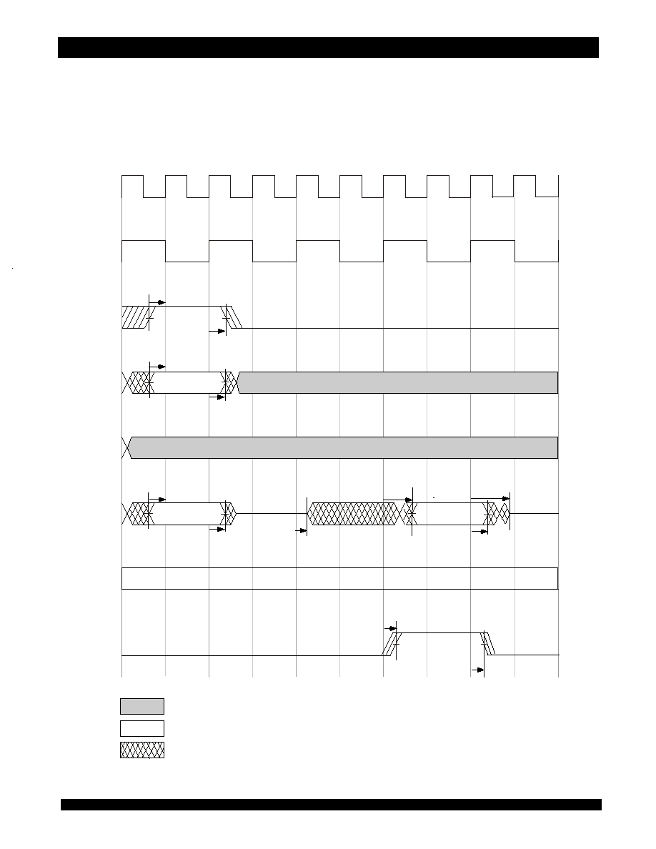
26
IDT75T43100
Preliminary Information
IP Co-Processor 32K Entries Commercial and Industrial Temperature Ranges
Output Timing (with IPC Read)
Timing Diagrams
CCLK
tH
tSU
REQSTB
CMD[3:0]
IP C R E A D
tSU
tH
REQDATA
Read Data
tCDC
(
MIN.
)
tCLZ
tSU
tH
Address
tCHZ
(
MAX.
)
(
MAX.
)
tCRD
(
MIN.
)
INDX
RDACK
tCRACK
(
MIN.
)
H5325 drw 03
Don't Care
Driven HIGH or LOW, but to an indeterminate state.
LOW impedance state.
tCRACK
(
MAX.
)
CMD[6:4]
CLK2X
t1
t2
t3
t4
t5
t6
t7
t8
t0
t9
(IPC READ)
6.42
27
IDT75T43100 Preliminary Information
IP Co-Processor 32K Entries Commercial and Industrial Temperature Ranges
Output Timing (with ZBT SRAM)
Timing Diagrams
NOTES:
1. CCLK is an internal signal not seen by the user.
2. The Index Bus is driven but to an indeterminate state.
3. Signal will drive LOW or HIGH depending on command; see sequence diagram for state.
4. This pin will be tied to the
CE input of ZBT and OE input will be tied LOW.
5. Refer to the SRAM datasheet for timing specifications.
6. HITACK and VALID signals can be valid based on the rising edge of CLK2X at time tCDV dependent on the Pipeline Delay (PD) value that
is programmed into the System Configuration Register (SCR). These signals will drive for 2 CLK2X cycles. A PD value of 3 is shown for
clarity. Typically, the PD would be set to 2.
7. RDACK signal can be valid based on the rising edge of CLK2X, at time tCRAK, dependent on the Pipeline Delay (PD)
value that is programmed into the System Configuration Register (SCR). This signal will drive for 2 CLK2X cycles. A PD value of 3 is shown
for clarity. Typically, the PD would be set to 2.
WE
SRAMDATA
HITACK
VALID
(MIN.)
t
CDC
NOTE 3
H5325 d04
(MAX.)
t
CDV
(MAX.)
t
CDV
(MIN.)
t
CDC
NOTE 3
RDACK
(7)
(M A X .)
t
C R A K
(MIN.)
t
CRAK
SRAM READ or
WRITE DATA
(NOTE 5)
t
CDV
(MIN.)
t
CDV
(MAX.)
NOTE 3
CE
/
OE
(4)
MATCHOUT
t
CMDV
(MIN.)
(MAX.)
t
CMDV
(MAX.)
t
CDV
.
VALID INDEX
(MIN.)
t
CDC
t
CIV
(MAX.)
INDX
NOTE 2
NOTE 2
CCLK
(1)
CLK2X
t9
t10
t11
t12
t13
t14
t8
(OUTPUT TIMING for
all commands except
IPC Read and Write)
t15
t16
(MIN.)
t
CDV
t18
t17
Pipeline Delay (PD)
(NOTE 6)
PD=0
PD=2
PD=3
PD=1
NOTE 3
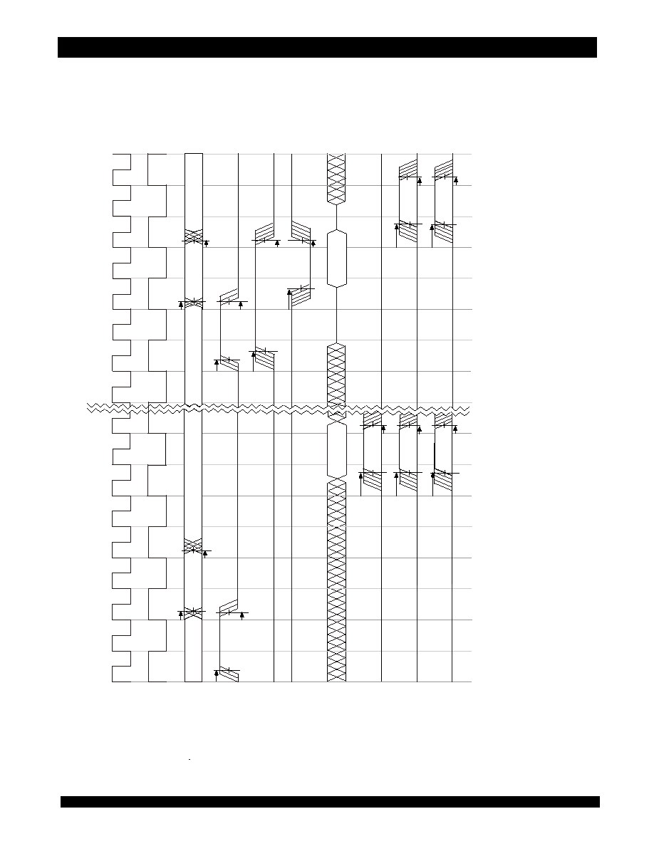
28
IDT75T43100
Preliminary Information
IP Co-Processor 32K Entries Commercial and Industrial Temperature Ranges
Timing Diagrams
Output Timing (with Synchronous Pipeline Burst)
NOTES:
1
.
CCLK is an internal signal not seen by the user.
2. The Index Bus is driven but to an indeterminate state.
3. Signal will drive LOW or HIGH depending on command; see sequence diagram for state.
4. This pin will be tied to the
OE
input of PBSRAM and
CE
input will be tied LOW.
5. Refer to the SRAM datasheet for timing specifications.
6. HITACK and VALID signals can be valid based on the rising edge of CLK2X at time tCDV dependent on the Pipeline Delay (PD) va
lue that is programmed into the System
Configuration Register (SCR). These signals will drive for 2 CLK2X cycles. A PD value of 2 is shown. Refer to Output Timing
(with ZBT SRAM) for the relative timing
of all PD values.
7
.
RDACK signal can be valid based on the rising edge of CLK2X, at time tCRAK, dependent on the Pipeline Delay (PD)
value that is programmed into the System Configuration Register (SCR). This signal will drive for 2 CLK2X cycles. A PD value
of 3 is shown for clarity. Typically, the
PD would be set to 2.
CLK2X
CCL
K
(1
)
W
E
S
RAMDATA
t 9
t 10
t 11
t 12
t 13
t 14
t 8
HITACK
(6
)
VA
L
I
D
(6
)
R
DAC
K
(7)
M
A
TCHO
UT
C
E
/
O
E
(
4
)
(
M
AX.
)
t
CI
V
VAL
I
D
I
NDEX
(
M
IN
.)
t
CD
C
t
CM
DV
(M
I
N
.
)
t
CM
D
V
(M
A
X
.
)
IND
X
(
M
AX.
)
t
CDV
(M
I
N
.
)
t
CDC
(M
A
X
.
)
t
CDV
(M
I
N
.
)
t
CD
C
NO
T
E
3
NO
T
E
3
NOT
E
3
(
M
AX.
)
t
CR
A
K
(M
I
N
.
)
t
CR
A
K
H
5325
d
0
5
t
CI
V
(M
A
X
.
)
VAL
I
D
I
NDEX
t
CDC
(M
I
N
.
)
t 81
t 82
t 83
t 84
t 85
t 86
t 80
NOT
E
2
t
CMD
V
(M
I
N
.
)
t
CM
D
V
(
M
AX.
)
(
M
IN
.)
t
CD
V
(M
A
X
.
)
t
CD
V
(M
I
N
.
)
t
CDV (M
A
X
.
)
t
CD
V
(N
O
T
E
5
)
t 15
t 78
t 79
NOT
E
2
NOT
E
2
SRA
M
W
R
I
T
E
D
ATA
.
.
NO
T
E
2
(N
O
T
E
5
)
(
Loo
k
u
p
S
R
A
M
R
ead
a
n
dN
oW
a
i
t
R
e
a
d
Ou
t
p
u
t
T
i
m
i
n
g
)
(
S
R
A
M
W
r
i
t
e
O
u
t
p
ut
T
i
m
i
ng
)
SR
A
M
RE
AD
D
A
T
A
(
M
AX.
)
t
CD
V
(M
I
N
.
)
t
CDC
(M
A
X
.
)
t
CD
V
(M
I
N
.
)
t
CDC
NO
T
E
3
NO
T
E
3
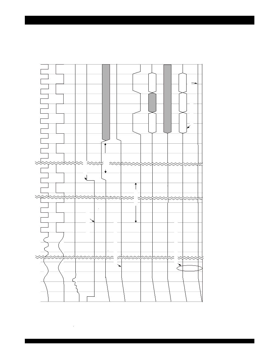
6.42
29
IDT75T43100 Preliminary Information
IP Co-Processor 32K Entries Commercial and Industrial Temperature Ranges
Reset/Initialization Sequence
Sequence Diagrams
CO
NF
I
G
U
R
A
T
I
O
N
R
E
G
I
ST
E
R
AD
D
R
E
S
S
WR
I
T
E
D
A
T
A
NE
X
T
CO
M
M
A
ND
A
D
D
R
ES
S
O
R
D
AT
A
N
EXT
C
O
MM
AN
D
IP
C
W
R
I
T
E
CO
M
M
A
N
D
B
egi
n
I
P
C
I
n
i
t
i
a
l
i
z
a
t
i
on
(
not
e
4
)
t 31
t 32
t 33
t 48
t 49
t 50
t 51
t 52
t 53
t 54
CL
K2X
CC
L
K
CM
D[
3
:
0]
RE
Q
D
A
T
A
CM
D[
6
:
4]
I5
3
2
5
d
r
w
0
1
OU
T
P
U
T
SIG
N
A
L
S
(5
)
(
R
ESET
/
I
N
I
T
I
A
L
I
Z
A
T
I
O
N
)
t 1
t 2
R
S
T
(1
)
t 0
V
DD
&V
DDQ
I
/
O
s
a
n
d
O
u
t
put
s
a
r
e
d
r
i
v
en
t
o
H
I
G
H
i
m
pedanc
e
s
t
a
t
e
(
not
e
2
)
CO
N
F
I
G
O
U
T
CO
NF
I
G
I
N
RE
Q
S
T
B
t 55
t 56
I
/
O
s
and
O
u
t
put
s
a
r
e
dr
i
v
en
t
o
H
I
G
H
i
m
pedanc
e
s
t
a
t
e
(
not
e
2
)
C
o
m
p
l
e
t
e
S
y
nc
hr
ono
us
R
e
s
e
t
16
Cy
c
l
es
Requi
r
e
d
32
Cy
c
l
e
s
R
equ
i
r
ed
B
egi
n
i
nt
er
nal
l
ogi
c
i
ni
t
i
al
i
z
at
i
o
n
(
no
t
e
3)
t 57
(N
o
t
e
6
)
NOTES:
1
.
Reset input,
RST
, must be driven Low during power up and before driving the clock and inputs.
2
.
After
RST
is Low and VDDQ supply ramps (stabilizes), all I/O's and outputs will be driven to a high impedance state asynchronously.
3
.
Synchronous reset of the internal logic and specific registers begins after clock stabilization and VDD and VDDQ supplies ram
p to operating levels. 32 CLK2X cycles are required
to fully reset from power up (Cold Reset) all internal logic and registers. Only 16 CLK2X cycles are required for a Hot Reset.
See Initialization for details.
4
.
IPC initialization can begin 16 CLK2X cycles after
RST
drives to HIGH. IPC Write commands set configuration registers and Data/Mask entries for required Implementation. See
Initialization for details.
5
.
The output signals consist of: INDX, MATCHOUT,
OE
/
CE
,
WE
, RDACK, HITACK and VALID.
6
.
The Index Bus remains in a high impedance state until the first command (a lookup or SRAM Access) which actively drives it to
a valid state. Afterwards the Index Bus will
always be driving to a valid state depending on the instruction.
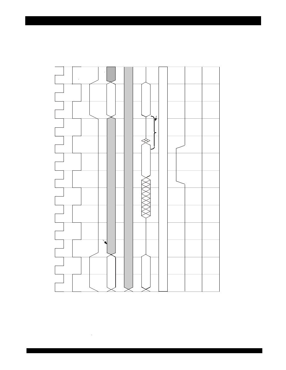
30
IDT75T43100
Preliminary Information
IP Co-Processor 32K Entries Commercial and Industrial Temperature Ranges
IPC Read (Register, Data, Mask)
NOTES:
1
.
CCLK is an internal signal not seen by the user.
2
.
The Index Bus is driven, but to an indeterminate state.
3
.
Commands initiated from t
2
to t
8
are ignored. The next command can be initiated at t
10
one cycle after the READ is complete. This allows for one bus turnaround cycle
on the Request Bus.
Sequence Diagrams
CL
K2
X
CC
L
K
(1
)
CM
D[
3
:
0
]
REQ
D
A
T
A
I
5
32
5
d
r
w
02
I
NDX
C
M
D
[
6:
4]
R
DACK
B
u
s
T
ur
nar
ound
C
ycl
e
HI
T
ACK
VA
L
I
D
t 1
t 2
t 3
t 4
t 5
t 6
t 7
t 8
t 0
RE
Q
S
T
B
t 9
t 10
t 11
T
h
e
n
ext
c
om
ma
nd
c
anno
t
b
e
i
n
i
t
iate
d
u
n
til
R
e
a
d
i
s
c
o
m
p
l
et
e
(
s
e
e
n
ot
e
3
)
(
I
PC
RE
A
D
)
IP
C
R
EA
D
CO
M
M
AND
REA
D
ADDRE
SS
NEX
T
CO
M
M
A
N
D
Ne
x
t
Co
m
m
a
n
d
,
A
d
dr
e
s
s
o
r
D
at
a
R
ead
D
a
t
a
NOT
E
2
t 12
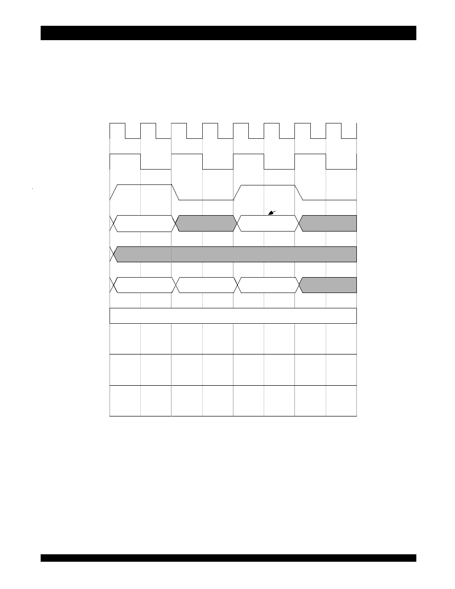
6.42
31
IDT75T43100 Preliminary Information
IP Co-Processor 32K Entries Commercial and Industrial Temperature Ranges
IPC Write (Register, Data, Mask)
Sequence Diagrams
NOTES:
1. CCLK is an internal signal not seen by the user.
2. The Index Bus is driven, but to an indeterminate state.
3. Next command can be initiated as early as the cycle t
4
.
CLK2X
CCLK
CMD[3:0]
REQDATA
I5325 drw03
INDX
CMD6:4]
RDACK
HITACK
VALID
t1
t2
t3
t4
t5
t6
t7
t0
REQSTB
(1)
NOTE 3
(IPC WRITE)
IPC WRITE
COMMAND
NEXT COMMAND
WRITE ADDRESS
WRITE DATA
NEXT COMMAND
ADDRESS OR DATA
NOTE 2
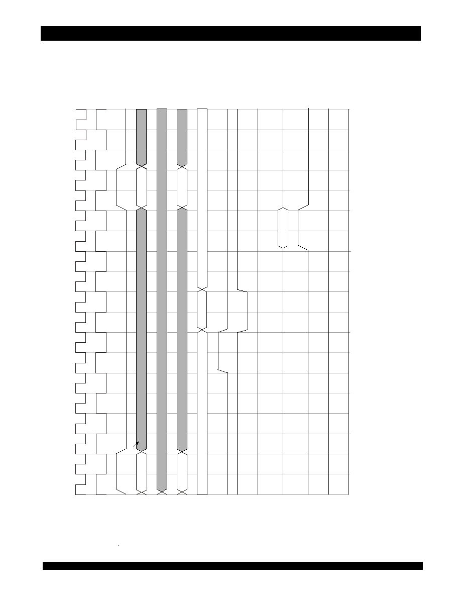
32
IDT75T43100
Preliminary Information
IP Co-Processor 32K Entries Commercial and Industrial Temperature Ranges
SRAM Read (ZBT)
Sequence Diagrams
NOTES:
1
.
CCLK is an internal signal not seen by the user.
2
.
Commands initiated from t
2
to t
12
are ignored. The next command can be initiated at t
14
, the following cycle after RDACK drives HIGH (Read is complete).
3
.
The Index Bus is driven, but to an indeterminate state.
4
.
For ZBT SRAM, the
OE
input is tied Low and the
CE
input is driven by the IPC
CE
/
OE
output..
5
.
RDACK signal can be valid based on the rising edge of CLK2X, at time tCRAK, dependent on the Pipeline Delay (PD)
value that is programmed into the System Configuration Register (SCR). This signal will drive for 2 CLK2X cycles. A PD value
of 3 is shown for clarity. Typically, the PD
would be set to 2.
N
E
X
T
CO
M
M
A
ND
ADDRESS
OR
DATA
F
O
R
N
EXT
CO
M
M
A
N
D
REQ
D
A
T
A
I5
3
2
5
d
r
w
0
5
I
NDE
X
I
NDX
MA
TCHO
UT
C
E
(4
)
SR
A
M
DA
TA
RDA
C
K
(5
)
VA
LI
D
SRAM
READ
DA
TA
CM
D[
6
:
4
]
W
E
HI
TA
CK
READ
A
DDRE
S
S
CL
K2
X
CCL
K
(1
)
CM
D[
3
:
0
]
t 1
t 2
t 3
t 4
t 5
t 6
t 7
t 8
t 0
t 9
t 10
t 11
t 12
t 13
t 14
t 15
t 16
RE
Q
S
TB
The
n
ext
c
om
m
a
nd
c
ann
ot
be
i
n
i
t
i
a
t
e
d
unt
i
l
R
ead
i
s
com
p
l
e
t
e
.
(
see
not
e
2
)
(S
R
A
M
R
E
A
D
)
SRAM
READ
COM
M
A
N
D
t 17
t 18
NOT
E
3
NOTE
3
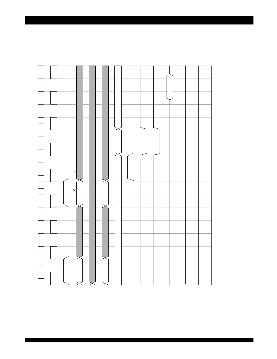
6.42
33
IDT75T43100 Preliminary Information
IP Co-Processor 32K Entries Commercial and Industrial Temperature Ranges
SRAM Write (ZBT)
Sequence Diagrams
NOTES:
1
.
CCLK is an internal signal not seen by the user.
2
.
The next command can be initiated during the cycle t
6
. Two dead cycles are inserted because a) write commands require one dead cycle before the next instruction
initiates, and b) the second cycles insures that no contention occurs on the SRAM Data Bus. If the next command is an IPC Read
, IPC Write or SRAM Write, it can
be initiated on the cycle t
4
.
3
.
The Index Bus is driven, but to an indeterminate state.
3
.
The Index Bus is driven, but to an indeterminate state.
4
.
For ZBT, the
OE
is tied LOW, and the
CE
input is driven by the IPC
CE
/
OE
output.
CL
K2
X
CC
L
K
(1
)
CMD
[
3:
0]
RE
QDA
T
A
IN
D
E
X
SR
A
M
W
R
IT
E
D
AT
A
IND
X
C
E
(4
)
W
E
HI
T
A
C
K
VA
L
I
D
,
I
5
32
5
d
r
w
06
RDA
C
K
W
R
I
T
E
A
DDR
E
S
S
N
E
X
T
CO
M
M
A
N
D,
AD
D
R
ES
S
O
R
D
A
T
A
t 1
t 2
t 3
t 4
t 5
t 6
t 7
t 8
t 0
t 9
M
A
T
CHOUT
RE
QS
T
B
CM
D[6:4]
t 10
t 11
t 12
t 13
t 14
t 15
t 16
No
t
e
2
SR
A
M
D
A
T
A
(S
RAM
W
R
I
T
E
)
SR
AM
W
R
I
T
E
CO
M
M
A
N
D
N
EXT
C
O
M
M
A
N
D
NO
T
E
3
NO
T
E
3

34
IDT75T43100
Preliminary Information
IP Co-Processor 32K Entries Commercial and Industrial Temperature Ranges
SRAM No Wait Read (ZBT)
Sequence Diagrams
NOTES:
1
.
CCLK is an internal signal not seen by the user.
2
.
The SRAM No Wait Read command does not require the user to wait until the Read is complete. The next commands can be initiat
ed as early as the following cycle
t
2
.
3
.
The Index Bus is driven, but to an indeterminate state.
4
.
For ZBT, the
OE
input is tied LOW, and the
CE
input is driven by the IPC
CE
/
OE
output.
5. HITACK and VALID signals can be valid based on the rising edge of CLK2X at time tCDV dependent on the Pipeline Delay (PD)
value that is programmed into the System
Configuration Register (SCR). These signals will drive for 2 CLK2X cycles. A PD value of 2 is shown. Refer to Output Timing
(with ZBT SRAM) for the relative timing
of all PD values.
I
NDE
X
SR
A
M
R
EAD
D
A
TA
REQ
D
A
T
A
IN
DX
MA
T
C
H
O
U
T
C
E
(4)
SRA
M
D
A
T
A
HI
T
A
CK
(5
)
VA
LI
D
(5
)
CM
D[
6
:
4
]
W
E
RDA
C
K
RE
AD
A
DDRES
S
ADDR
ESS
O
R
DAT
A
FO
R
N
EXT
CO
M
M
A
N
D
CL
K
2
X
CC
L
K
(1
)
CM
D[
3
:
0
]
I5
325
d
r
w
07
t 1
t 2
t 3
t 4
t 5
t 6
t 7
t 8
t 0
t 9
t 10
t 11
t 12
t 13
t 14
t 15
t 16
RE
Q
S
T
B
N
e
xt
command
c
a
n
b
e
i
ni
t
i
a
t
ed
t
h
is
cycle.
(
S
ee
not
e
2
)
(
S
R
A
MN
oW
a
i
t
R
e
a
d
)
S
R
AM
ACCE
SS
CO
M
M
AND
NEXT
C
O
M
M
A
N
D
NO
T
E
3
NOT
E
3
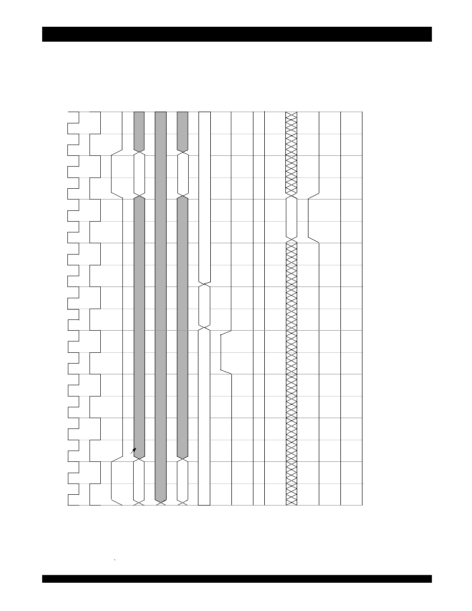
6.42
35
IDT75T43100 Preliminary Information
IP Co-Processor 32K Entries Commercial and Industrial Temperature Ranges
SRAM Read (PBSRAM)
Sequence Diagrams
NOTES:
1
.
CCLK is an internal signal not seen by the user.
2
.
Commands initiated from t
2
to t
12
are ignored. The next command can be initiated at t
14
, the following cycle after RDACK drives HIGH (Read is complete).
3
.
The Index Bus is driven, but to an indeterminate state.
4
.
For Synchronous Pipelined Burst SRAM, the
CE
input is tied LOW,
ADSP
is tied HIGH,
ADSC
Is tied LOW and the
OE
input is driven by the IPC
CE
/
OE
output.
5
.
RDACK signal can be valid based on the rising edge of CLK2X, at time tCRAK, dependent on the Pipeline Delay (PD)
value that is programmed into the System Configuration Register (SCR). This signal will drive for 2 CLK2X cycles. A PD value
of 3 is shown for clarity. Typically, the PD
would be set to 2.
N
EXT
CO
M
M
A
N
D
ADDR
ESS
O
R
DAT
A
F
O
R
N
E
X
T
C
O
MMA
N
D
RE
QD
A
T
A
I5
32
5
d
r
w
0
9
IN
D
E
X
IN
DX
MA
T
C
H
O
U
T
O
E
(4
)
SR
AM
REA
D
D
A
T
A
SRA
M
DA
TA
RD
A
C
K
(5
)
VA
LI
D
CM
D[
6
:
4
]
W
E
HI
T
A
C
K
R
EAD
ADDR
ESS
CL
K
2
X
CC
L
K
(1
)
CM
D[
3
:
0
]
t 1
t 2
t 3
t 4
t 5
t 6
t 7
t 8
t 0
t 9
t 10
t 11
t 12
t 13
t 14
t 15
t 16
RE
QST
B
T
h
e
nex
t
c
om
mand
c
annot
be
ini
t
iated
until
R
e
ad
i
s
com
p
lete.
(
s
e
e
note
2
)
(
S
RA
M
R
E
A
D)
SR
A
M
R
E
AD
CO
M
M
A
N
D
t 17
NO
T
E
3
NO
T
E
3
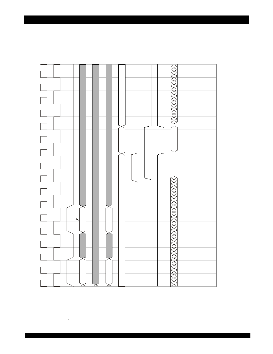
36
IDT75T43100
Preliminary Information
IP Co-Processor 32K Entries Commercial and Industrial Temperature Ranges
SRAM Write (PBSRAM)
Sequence Diagrams
NOTES:
1
.
CCLK is an internal signal not seen by the user.
2
.
The next command can be initiated during the cycle t
4
. Write commands require one dead cycle before the next instruction intiates.
3
.
The Index Bus is driven, but to an indeterminate state.
4
.
For -Synchronous Pipeline Burst SRAM, the
CE
is tied LOW,
ADSP
is tied HIGH,
ADSC
is tied LOW, and the
OE
input is driven by the IPC
CE
/
OE
output.
B
CLK2X
CC
L
K
(1
)
CMD[3:
0]
R
E
Q
DAT
A
INDE
X
SR
A
M
W
R
I
T
E
D
AT
A
INDX
O
E
(4
)
W
E
HITA
CK
VA
L
I
D
I5
32
5
d
r
w
10
RDA
CK
W
R
I
T
E
A
DDRESS
N
E
XT
CO
M
M
AND,
A
DDR
E
S
S
O
R
D
A
T
A
t 1
t 2
t 3
t 4
t 5
t 6
t 7
t 8
t 0
t 9
MA
TCHO
U
T
RE
Q
S
T
B
CMD[
6:
4]
t 10
t 11
t 12
t 13
t 14
t 15
t 16
NO
TE
2
SR
A
M
D
A
T
A
(
S
RA
M
W
RITE
)
SR
A
M
W
R
I
T
E
CO
M
M
A
N
D
NE
X
T
CO
M
M
A
N
D
NO
TE
3
NO
T
E
3
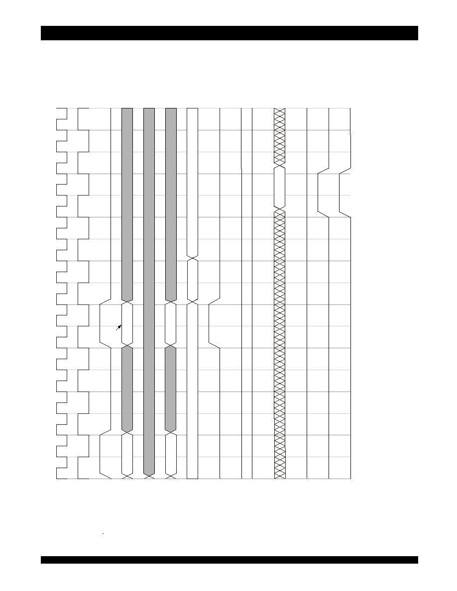
6.42
37
IDT75T43100 Preliminary Information
IP Co-Processor 32K Entries Commercial and Industrial Temperature Ranges
SRAM No Wait Read (PBSRAM)
Sequence Diagrams
NOTES:
1
.
CCLK is an internal signal not seen by the user.
2
.
The SRAM No Wait Read command does not require the user to wait until the Read is complete. If the next command is a SRAM Wri
te, it can be initiated during the cycle
t
6
. Two dead cycles are inserted to insure that no contention occurs on the SRAM Data Bus. All other commands can be initiated
on the cycle t
2
.
3
.
The Index Bus is driven, but to an indeterminate state.
4
.
For Synchronous Pipeline Burst SRAM, the
CE
input is tied Low,
ADSP
is tied HIGH,
ADSC
is tied LOW, and the
OE
input is driven by the IPC
CE
/
OE
output.
5. HITACK and VALID signals can be valid based on the rising edge of CLK2X at time tCDV dependent on the Pipeline Delay (PD) v
alue that is programmed into the System
Configuration Register (SCR). These signals will drive for 2 CLK2X cycles. A PD value of 2 is shown. Refer to Output Timing
(with ZBT SRAM) for the relative timing
of all PD values.
INDE
X
SR
A
M
R
EAD
D
A
T
A
RE
Q
D
A
T
A
I
5325
d
r
w
1
1
IND
X
MA
T
C
H
O
UT
O
E
(4
)
SR
A
M
D
A
T
A
HIT
A
CK
(5
)
VA
L
I
D
(5
)
CM
D[6:
4]
W
E
RDA
CK
R
EAD
AD
D
R
ESS
A
DDRE
S
S
O
R
DA
T
A
F
O
R
N
E
X
T
CO
M
M
A
ND
CLK2X
CC
L
K
(1
)
CM
D[3:0]
t 1
t 2
t 3
t 4
t 5
t 6
t 7
t 8
t 0
t 9
t 10
t 11
t 12
t 13
t 14
t 15
t 16
RE
Q
S
TB
N
e
x
t
c
o
m
m
and
c
a
n
b
e
i
ni
t
i
at
ed
t
h
i
s
c
y
c
l
e.
(S
ee
not
e
2
)
(
S
R
A
M
N
o
W
a
i
t
R
ead
)
S
R
AM
AC
C
E
SS
CO
M
M
A
ND
NE
X
T
C
O
M
M
A
N
D
NO
T
E
3
NO
T
E
3
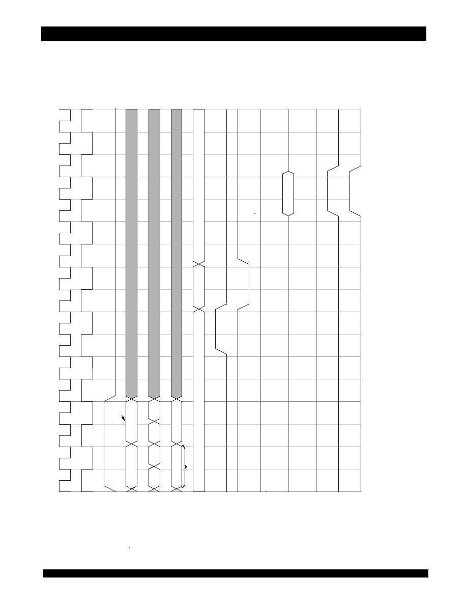
38
IDT75T43100
Preliminary Information
IP Co-Processor 32K Entries Commercial and Industrial Temperature Ranges
72-Bit Lookup (with ZBT SRAM)
(5)
Sequence Diagrams
NOTES:
1
.
CCLK is an internal signal not seen by the user.
2
.
Next command can be initiated during cycle t
2
.
3
.
The Index Bus is driven, but to an indeterminate state.
4
.
For ZBT SRAM, the
OE
input is tied Low and the
CE
input is driven by the IPC
CE
/
OE
output.
5
.
For Synchronous Pipelined Burst SRAM sequence see Output Timing diagram (with PBSRAM).
6. HITACK and VALID signals can be valid based on the rising edge of CLK2X at time tCDV dependent on the Pipeline Delay (PD) va
lue that is programmed into the System
Configuration Register (SCR). These signals will drive for 2 CLK2X cycles. A PD value of 2 is shown. Refer to Output Timing
(with ZBT SRAM) for the relative timing
of all PD values.
CL
K2X
CCL
K
(1
)
RE
Q
D
A
T
A
I
5325
d13
VA
L
I
D
(6
)
SR
AM
R
E
AD
D
A
T
A
HI
T
A
C
K
(6
)
RDA
CK
INDX
CE
(4
)
MA
T
CHO
U
T
SR
A
M
D
A
T
A
CMD[6
:
4]
IN
DEX
B
I
T
S
71:
0
NE
X
T
CO
M
M
A
N
D
A
D
DRE
S
S
O
R
DA
T
A
7
2
BI
T
M
AT
C
H
D
A
T
A
GM
R
RE
GI
S
T
E
R
SR
R
RE
G
I
S
T
E
R
N
EXT
G
M
R
R
E
G
I
STER
NE
X
T
SRR
R
E
GI
ST
ER
WE
RE
Q
S
TB
t 1
t 2
t 3
t 4
t 5
t 6
t 7
t 8
t 0
(7
2
B
I
T
L
O
O
K
U
P
)
t 9
t 10
t 11
t 12
t 13
t 14
t 15
t 16
72
B
I
T
L
OOK
U
P
CO
M
M
A
N
D
NE
X
T
CO
M
M
A
ND
NO
T
E
2
NO
T
E
3
NO
T
E
3
CM
D[3:
0]

6.42
39
IDT75T43100 Preliminary Information
IP Co-Processor 32K Entries Commercial and Industrial Temperature Ranges
144-Bit Lookup (with ZBT SRAM)
(5)
Sequence Diagrams
NOTES:
1
.
CCLK is an internal signal not seen by the user.
2. Next command can be initiated during cycle (t
2
)
.
3
.
The Index Bus is driven, but to an indeterminate state.
4
.
For ZBT SRAM, the
OE
input is tied Low and the
CE
input is driven by the IPC
CE
/
OE
output.
5. For Synchronous Pipelined Burst SRAM sequence see Output Timing diagram (with PBSRAM).
6. HITACK and VALID signals can be valid based on the rising edge of CLK2X at time tCDV dependent on the Pipeline Delay (PD) va
lue that is programmed into the System
Configuration Register (SCR). These signals will drive for 2 CLK2X cycles. A PD value of 2 is shown. Refer to Output Timing
(with ZBT SRAM) for the relative timing of
all PD values.
CL
K2
X
CC
L
K
(1
)
C
M
D[
3:
0]
RE
Q
D
A
T
A
I
5325
d14
VA
L
I
D
(6
)
HI
TA
C
K
(6
)
RD
A
C
K
IN
D
X
CE
(4
)
MA
T
C
H
O
UT
C
M
D[
6:
4]
GM
R
REG
I
STER
SR
R
R
E
G
I
ST
ER
I
NDE
X
NE
X
T
CO
M
M
A
ND
A
DDR
E
S
S
O
R
D
A
T
A
1
4
4
BIT
M
AT
C
H
D
A
T
A
NEXT
G
M
R
REG
I
ST
ER
N
E
XT
SR
R
REG
I
S
T
ER
WE
SR
A
M
D
A
T
A
RE
Q
S
T
B
t 1
t 2
t 3
t 4
t 5
t 6
t 7
t 8
t 0
(
1
4
4
B
I
T
LOOK
U
P
)
t 9
t 10
t 11
t 12
t 13
t 14
t 15
t 16
144
B
I
T
L
OOK
UP
CO
M
M
A
N
D
NE
X
T
CO
M
M
A
N
D
NO
T
E
2
BI
T
S
71:
0
BI
T
S
144:
72
SR
A
M
R
E
AD
D
A
T
A
NO
T
E
3
NO
T
E
3
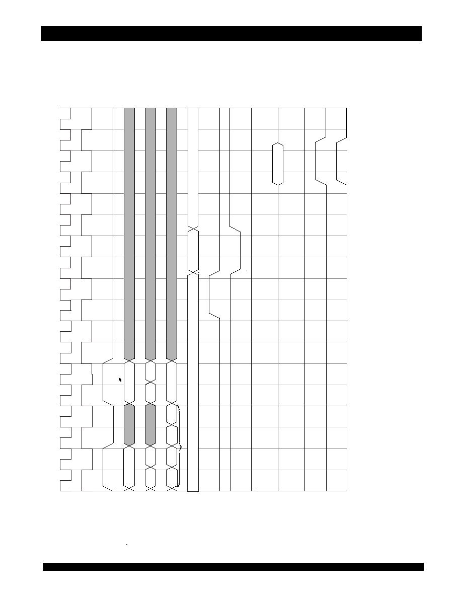
40
IDT75T43100
Preliminary Information
IP Co-Processor 32K Entries Commercial and Industrial Temperature Ranges
288-Bit Lookup (with ZBT SRAM)
(5)
Sequence Diagrams
NOTES:
1
.
CCLK is an internal signal not seen by the user.
2
.
Next command can be initiated during cycle t
4
.
3
.
The Index Bus is driven, but to an indeterminate state.
4
.
For ZBT SRAM, the
OE
input is tied Low and the
CE
input is driven by the IPC
CE
/
OE
output.
5
.
For Synchronous Pipelined Burst SRAM sequence see Output Timing diagram (with PBSRAM).
6. HITACK and VALID signals can be valid based on the rising edge of CLK2X at time tCDV dependent on the Pipeline Delay (PD) va
lue that is programmed into the System
Configuration Register (SCR). These signals will drive for 2 CLK2X cycles. A PD value of 2 is shown. Refer to Output Timing
(with ZBT SRAM) for the relative timing of
all PD values.
CL
K2
X
CC
L
K
(1
)
CM
D
[
3:
0]
REQ
D
A
T
A
I5
325
d15
VA
L
I
D
(6
)
SRAM
READ
DATA
HI
T
A
CK
(6
)
RDA
CK
INDX
IN
D
E
X
CE
(4)
M
A
T
CHO
UT
SR
A
M
D
A
T
A
CM
D
[
6:
4]
N
EXT
G
M
R
R
E
G
I
ST
ER
NEXT
SRR
REGI
ST
E
R
NEX
T
COM
M
A
N
D
A
D
DRE
S
S
OR
DAT
A
2
8
8
BI
T
M
A
T
CH
DA
T
A
GM
R
R
E
GIS
T
E
R
SR
R
RE
GI
ST
E
R
WE
B
IT
S
287
:216
B
IT
S
71:0
B
IT
S
14
3:72
B
IT
S
215:144
RE
Q
S
T
B
t 1
t 2
t 3
t 4
t 5
t 6
t 7
t 8
t 0
(
2
8
8
BIT
LO
O
K
UP
)
t 9
t 10
t 11
t 12
t 13
t 14
t 15
t 16
288
B
I
T
L
O
O
K
U
P
CO
M
M
A
N
D
NEXT
CO
M
M
AND
NO
T
E
2
NO
T
E
3
NOT
E
3
t 1
7
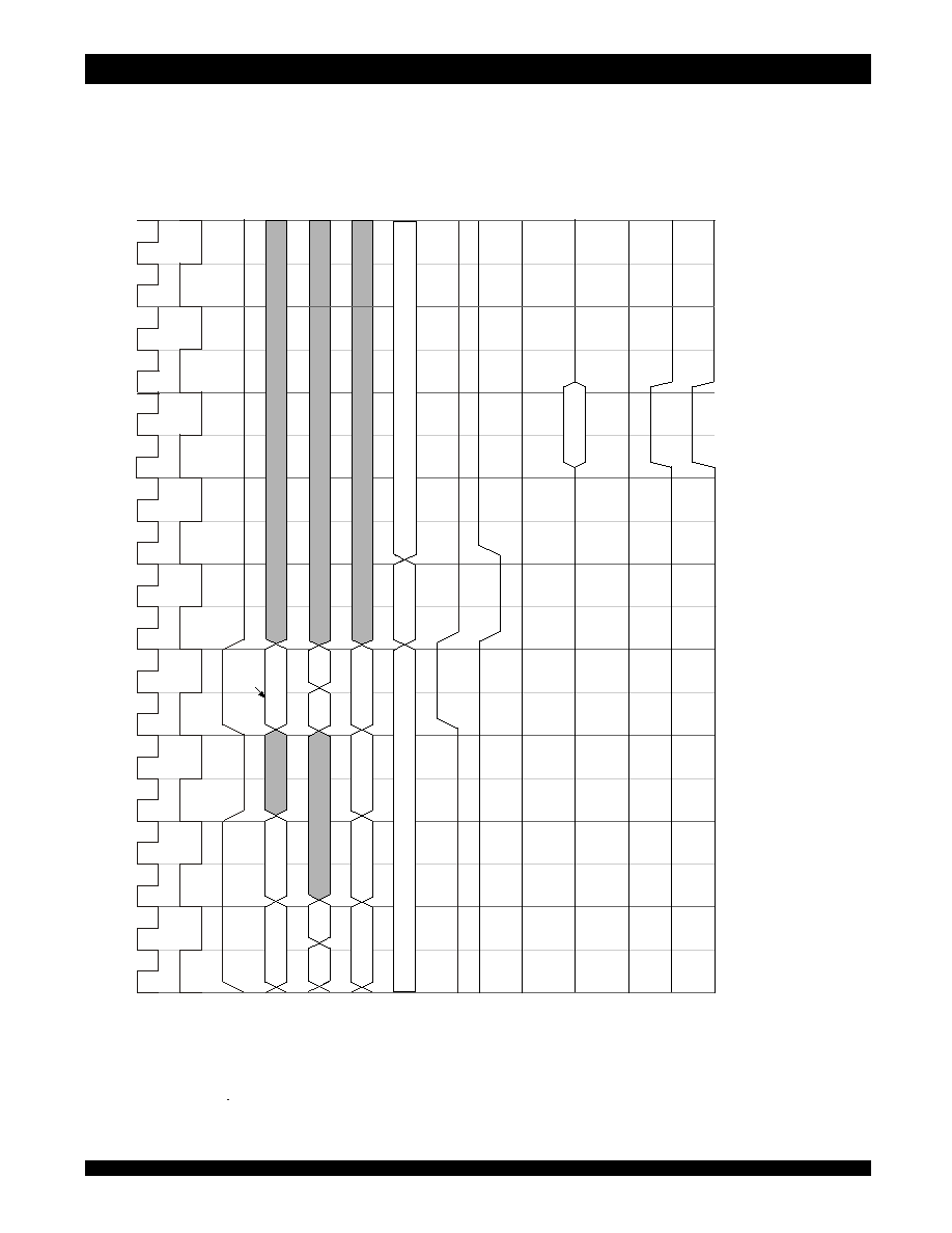
6.42
41
IDT75T43100 Preliminary Information
IP Co-Processor 32K Entries Commercial and Industrial Temperature Ranges
72 Bit Lookup Followed by an IPC Write (with ZBT SRAM)
(5)
Sequence Diagrams
NOTES:
1
.
CCLK is an internal signal not seen by the user.
2
.
Next command can be initiated during cycle t
6.
3
.
The Index Bus is driven, but to an indeterminate state.
4
.
For ZBT SRAM, the
OE
input is tied Low and the
CE
input is driven by the IPC
CE
/
OE
output.
5
.
For Synchronous Pipelined Burst SRAM sequence see Output Timing diagram (with PBSRAM).
6. HITACK and VALID signals can be valid based on the rising edge of CLK2X at time tCDV dependent on the Pipeline Delay (PD) va
lue that is programmed into the System
Configuration Register (SCR). These signals will drive for 2 CLK2X cycles. A PD value of 2 is shown. Refer to Output Timing
(with ZBT SRAM) for the relative timing
of all PD values.
CL
K
2
X
CCL
K
(1
)
C
M
D
[
3:
0]
RE
Q
D
A
T
A
72-
B
I
T
L
O
O
K
U
P
I
NDE
X
I
5
32
5
d
r
w
22
SRA
M
R
E
AD
D
A
T
A
VA
LID
(6
)
C
E
(4
)
W
E
RDA
CK
H
ITA
C
K
(6
)
IN
D
X
C
M
D
[
6:
4]
SRA
M
D
A
T
A
NE
XT
C
O
M
M
A
N
D,
A
D
DR
ESS
OR
DA
T
A
GM
R
RE
G
I
S
T
E
R
SR
R
R
E
GI
ST
ER
NE
W
G
MR
RE
G
I
S
T
E
R
NE
W
S
R
R
R
E
GIST
E
R
MA
T
CHO
UT
t 1
t 2
t 3
t 4
t 5
t 6
t 7
t 8
t 0
t 1
t 2
t 3
t 4
t 5
t 6
t 7
t 8
t 0
(72
b
i
t
l
ook
up)
(
I
PC
W
R
IT
E)
IP
C
W
RIT
E
CO
M
M
AN
D
R
E
Q
S
T
B
7
2
-
B
it
L
O
O
K
UP
COM
M
AND
IP
C
W
RI
T
E
CO
M
M
A
ND
N
EXT
CO
M
M
A
ND
NOT
E
2
t 9
t 10
t 11
t 12
t 13
t 14
t 15
7
2
-B
I
T
MA
T
C
H
DAT
A
W
R
I
T
E
A
DD
RE
SS
WR
I
T
E
D
A
T
A
NO
T
E
3
NOT
E
3
42
IDT75T43100
Preliminary Information
IP Co-Processor 32K Entries Commercial and Industrial Temperature Ranges
JTAG Interface Specification
JTAG InterfaceSpecification
TCK
Device Inputs
(1)
/
TDI/TMS
Device Outputs
(2)
/
TDO
TRST
(3)
t
JCD
t
JDC
t
JRST
t
JS
t
JH
t
JCYC
t
JRSR
t
JF
t
JCL
t
JR
t
JCH
M5325 drw 01
x
Symbol
Parameter
Min.
Max.
Units
t
JCYC
JTAG Clock Input Period
100
____
ns
t
JCH
JTAG Clock HIGH
40
____
ns
t
JCL
JTAG Clock Low
40
____
ns
t
JR
JTAG Clock Rise Time
____
3
(1)
ns
t
JF
JTAG Clock Fall Time
____
3
(1)
ns
t
JRST
JTAG Reset
100
____
ns
t
JRSR
JTAG Reset Recovery
100
____
ns
t
JCD
JTAG Data Output
____
20
ns
t
JDC
JTAG Data Output Hold
0
____
ns
t
JS
JTAG Setup
15
____
ns
t
JH
JTAG Hold
15
____
ns
I5325 tbl 01
Register Name
Bit Size
Instruction (IR)
4
Bypass (BYR)
1
JTAG Identification (JIDR)
32
Boundary Scan (BSR)
Note (1)
I5325 tbl 03
NOTES:
1. Device inputs = All device inputs except TDI, TMS and
TRST.
2. Device outputs = All device outputs except TDO.
3. During power up,
TRST should be driven low.
NOTE:
1. The Boundary Scan Descriptive Language (BSDL) file for this device is available
by contacting your local IDT sales representative.
JTAG AC Electrical
Characteristics
(1,2,3,4)
Scan Register Sizes
NOTES:
1. Guaranteed by design.
2. AC Test Load (stated earlier in this document) on external output signals.
3. Refer to AC Test Conditions stated earlier in this document.
4. JTAG operations occur at one speed (10MHz). The base device may run at
any speed specified in this datasheet.
6.42
43
IDT75T43100 Preliminary Information
IP Co-Processor 32K Entries Commercial and Industrial Temperature Ranges
JTAG Identification Register Definitions
JTAG InterfaceSpecification
Instruction Field
Value
Description
Revision Number (31:28)
0x1
Reserved for version number
IDT Device ID (27:12)
0x200
Defines IDT part number
IDT JEDEC ID (11:1)
0x33
Allows unique identification of device vendor as IDT
ID Register Indicator Bit (Bit 0)
1
Indicates the presenc e of an ID register
I5325 tbl 02
Instruction
Description
O P CO DE
E XTE S T
(3)
Fo rc e s c o nte nts o f the b o und ary s c an c e lls o nto the d e v ic e o utp uts
(1,3)
.
P lac e s the b o und ary s c an re g is te r (B S R ) b e twe e n TD I and TD O .
0000
S A M P LE /P RE LO A D
P lac e s the b o und ary s c an re g is te r (B S R ) b e twe e n TD I and TD O .
S A M P LE allo ws d ata fro m d e v ic e inp uts
(2)
and o utp uts
(1)
to b e c ap ture d
in the b o und ary s c an c e lls and shifte d s e rially thro ug h TDO . P RE LO A D
allo w s d ata to b e inp ut s e rially into the b o und ary s c an c e lls v ia the TDI.
0001
DE V IC E _ID
Lo ad s the J TA G ID re g is te r (J IDR) with th e v e nd o r ID c o d e and p lac e s
the re g is te r b e twe e n TDI and TDO .
0010
HIG HZ
P lac e s the b y p as s re g is te r (B Y R) b e twe e n TDI and TDO . F o rc e s all
d e v ic e o utp ut d riv e rs to a H ig h-Z s tate .
0011
RE S E RV E D
S e v e ral c o m b inatio ns are re s e rv e d . Do n o t us e c o d e s o the r than tho s e
id e ntifie d fo r E XTE S T, S A M P LE /P RE LO A D, D E V ICE _ID, HIG H Z, CLA M P,
VA LIDATE and B Y PA S S ins tructio ns .
0100
RE S E RV E D
0101
RE S E RV E D
0110
RE S E RV E D
0111
CLA M P
Us e s B Y R . Fo rc e s c o nte nts o f the b o und ary s c an c e lls o nto the d e v ic e
o utp uts . P lac e s the b y p as s re g is te r (B Y R ) b e twe e n TDI and TD O .
1000
RE S E RV E D
S am e as ab o v e .
1001
RE S E RV E D
1010
RE S E RV E D
1011
RE S E RV E D
1100
VA LIDATE
A uto m atic ally lo ad e d into the ins truc tio n re g is te r whe ne v e r the TA P
c o ntro lle r p as s e s thro ug h the C A P TU RE -IR s tate . The lo w e r two b its '01'
are m and ate d b y the IE E E s td . 1149.1 s p e c ific atio n.
1101
RE S E RV E D
S am e as ab o v e .
1110
B Y PA S S
The B Y PA S S ins truc tio n is u s e d to trunc ate the b o und ary s c an re g is te r
as a sing le b it in le ng th.
1111
I5325 tbl 04
Available JTAG Instructions
NOTES:
1. Device outputs = All device outputs except TDO.
2. Device inputs = All device inputs except TDI, TMS and
TRST.
3. The IDT75T43100 supports a user-designed Bidirectional Boundary Scan Cell, in compliance with IEEE Standard 1149.1b-1994, for each of the REQDATA
signals. When using these Bidirectional cells acting as outputs, while EXTEST is in effect, the capture flip-flop loads a 0 (ZERO) data at the CAPTURE-DR
state. Refer to the Boundary Scan Descriptive Language (BSDL) file for a detailed description of the cell.
44
IDT75T43100
Preliminary Information
IP Co-Processor 32K Entries Commercial and Industrial Temperature Ranges
Package Diagram Outline - 304 Ball Grid Array
Package Diagram Outline
6.42
45
IDT75T43100 Preliminary Information
IP Co-Processor 32K Entries Commercial and Industrial Temperature Ranges
Ordering Information
Ordering Information
304 Ball Grid Array (BGA)
S
Power
X
Speed
XX
Package
BS
IDT
XXX
50
66
L5325 drw 01
Device
Type
75T43100
Mega Lookups per second
,
X
X
Process/
Temperature
Range
Blank
I
Commercial (0
o
C to +70
o
C)
Industrial (-40
o
C to +85
o
C)
CORPORATE HEADQUARTERS
for SALES:
for Tech Support:
2975 Stender Way
831-754-4555
ipchelp@idt.com
Santa Clara, CA 95054
fax: 831-754-4547
831-754-4555
www.idt.com
The IDT logo is a registered trademark of Integrated Device Technology, Inc.
ZBT
Æ
and Zero Bus Turnaround are trademarks of Integrated Device Technology, Inc. and the architecture is supported by Micron Technology and Motorola Inc.

46
IDT75T43100
Preliminary Information
IP Co-Processor 32K Entries Commercial and Industrial Temperature Ranges
Revision History
Revision History
REV
DATE
PAGES
DESCRIPTION
00
06/01/2001
1 - 46
Preliminary Information Datasheet, Public Release
01
07/09/2001
p. 1,9,45
Added Industrial Temperature
p. 9
Modify the Power #'s (Refer to Errata Notification # SREN-01-01)
p. 18
Clarified Figure 3.2, Read & Writes of Registers (Refer to Errata Notification # SREN-01-02)