 | –≠–ª–µ–∫—Ç—Ä–æ–Ω–Ω—ã–π –∫–æ–º–ø–æ–Ω–µ–Ω—Ç: 77V107 | –°–∫–∞—á–∞—Ç—å:  PDF PDF  ZIP ZIP |
1 of 24
July 3, 2001
2001 Integrated Device Technology, Inc.
DSC 5362/2
Single ATM PHY for 25.6 and
51.2 Mbps with Utopia Level 2
Features List
Features List
Features List
Features List
!
Performs the PHY-Transmission Convergence (TC) and
Physical Media Dependent (PMD) Sublayer functions of the
Physical Layer
!
Compliant to ATM Forum (af-phy-040.000) and ITU-T I.432.5
specifications for 25.6 Mbps physical interface
!
Also operates at 51.2Mbps
!
8-bit Utopia Level 2 Interface
!
3-Cell Transmit & Receive FIFOs
!
Receiver Auto-Synchronization and Good Signal Indication
!
Supports UTP Category 3 physical media
!
Interfaces to standard magnetics
!
Low-Power CMOS
!
3.3V supply with 5V tolerant inputs
!
100-lead TQFP Package (14 x 14 mm)
!
Commercial and Industrial temperature ranges
D
D
D
Description
escription
escription
escription
The IDT77V107 is a member of IDT's family of products supporting
Asynchronous Transfer Mode (ATM) data communications and
networking. The IDT77V107 implements the physical layer for 25.6
Mbps ATM, connecting a serial copper link (UTP Category 3) to an ATM
layer device such as a SAR or a switch ASIC. The IDT77V107 also
operates at 51.2 Mbps and is well suited to backplane driving applica-
tions. The 77V107 has an 8-bit UTOPIA Level 2 interface on the cell
side.
The IDT77V107 is fabricated using IDT's state-of-the-art CMOS tech-
nology, providing the highest levels of integration, performance and reli-
ability, with the low-power consumption characteristics of CMOS.
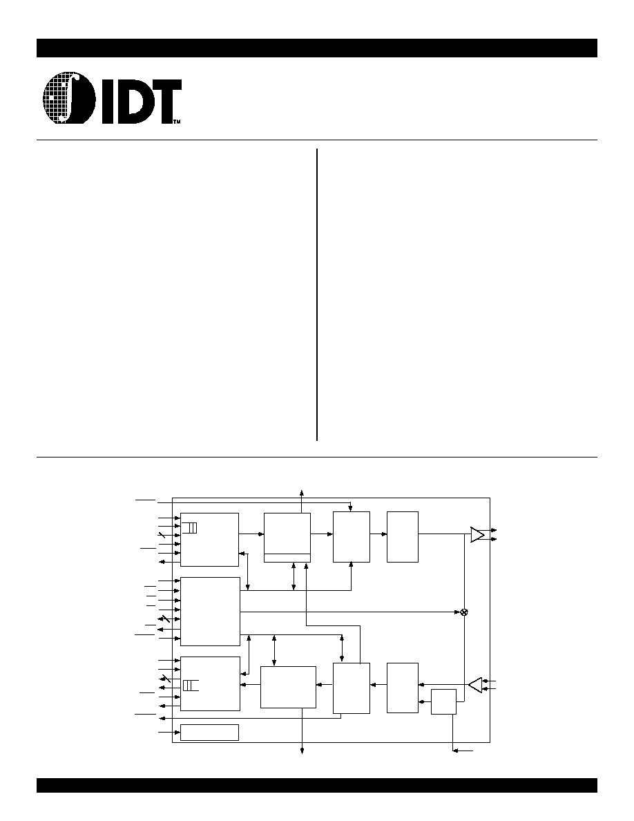
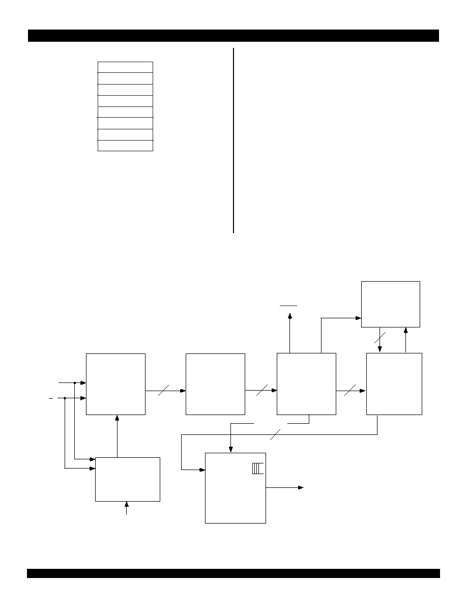
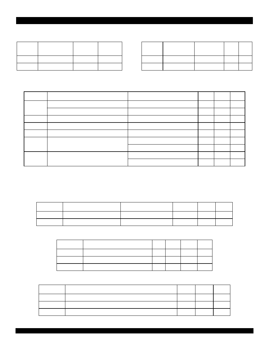
77V107 Overview
77V107 Overview
77V107 Overview
77V107 Overview
The 77V107 is a physical layer interface chip for 25.6Mbps ATM
network communications as defined by ATM Forum document af-phy-
040.000 and ITU-T I.432.5. The physical layer is divided into a Physical
Media Dependent sub layer (PMD) and Transmission Convergence (TC)
sub layer. It is based on the 77V106.
The PMD sub layer includes the functions for the transmitter, receiver
and clock recovery for operation across 100 meters of category 3
unshielded twisted pair (UTP) cable. This is referred to as the Line Side
Interface.
The TC sub layer defines the line coding, scrambling, data framing
and synchronization. Transmitted cells are first scrambled, then pass
through a 4b5b encoder and are finally NRZI encoded. In the 4b5b
encoder, 4-bit nibbles are converted to 5-bit symbols via a look-up table.
In addition to the 16 valid data symbols, a 17th symbol is used for a
special escape (X) symbol. This symbol has the property of being
Functional Block Diagram
Functional Block Diagram
Functional Block Diagram
Functional Block Diagram
TxREF
TxDATA
TxSOC
TxE N
ALE
RXCLAV
W R
R D
C S
AD[7:0]
I NT
RxDATA
RxSOC
R xE N
TXCLAV
RxR EF
3 CELL FIFO
9
8
9
UTILITY
BUS
CONTROLLER
3 CELL FIFO
SCRAMBLER
PRNG
DESCRAMBLER
5B/4B
DECODER
S/P
DNRZI
4B/5B
ENCODER
P/S
NRZI
CLK
REC
TXD+
Line
Driver
TXD-
Line
RxVR
RxD+
RxD-
LOOP BACK
RESET
RxLED
OSC
77V107
5362 drw 01
TxLED
RESET
TxCLK
RxCLK
TxAddr[4:0]
RxAddr[4:0]
M1, M0
MODE SELECT
IDT77V107
2 of 24
July 3, 2001
IDT77V107
uniquely defined such that this bit sequence cannot be duplicated by
concatenating any two other valid symbols. The escape symbol is used
incombination with a second symbol to form command symbol pairs.
Two command symbol pairs are defined as start-of-cell indicators, and
one is used as the 8kHz timing marker.
In the absence of a cell to transmit, the TC will continue to generate
valid symbols which are then transmitted across the line. When a
complete cell is available for transmission, the TC transmits the appro-
priate start-of-cell command symbol pair followed immediately the the
scrambled and encoded 53-byte cell. A falling edge on the TxREF pin
results in the insertion of an 8kHz timing marker in the transmit stream.
The receiver PMD performs clock and data recovery. The TC
achieves symbol framing (as described below). Start-of-cell command
symbol pairs and 8kHz timing symbol pair are handled appropriately,
with receive cells being placed into the receive FIFO.
On the cell side, the 77V107 connects to an ATM layer device (such
as a switch core or SAR) through an 8-bit Utopia Level 2 interface.
An 8-bit muxed address and data bus, controlled by a conventional
asynchronous read/write handshake, provides software access to
numerous internal control and status registers.
Additional pins permit insertion and extraction of an 8kHz timing
marker, and provide LED indication of receive and transmit status.
Auto-Synchronization and Good
Auto-Synchronization and Good
Auto-Synchronization and Good
Auto-Synchronization and Good
Signal Indication
Signal Indication
Signal Indication
Signal Indication
The 77V107 features a new receiver synchronization algorithm that
allows it to achieve 4b5b symbol framing on any valid data stream. This
is an improvement on earlier products which could frame only on the
escape symbol, which occurs only in start-of-cell or 8kHz (X8) timing
marker symbol pairs.
ATM25 transceivers always transmit valid 4b5b symbols, allowing
the 77V107 receive section to achieve symbol framing and properly indi-
cate receive signal status, even in the absence of ATM cells or 8kHz
(X8) timing markers in the receive data stream. A state machine moni-
tors the received symbols and asserts the "Good Signal" status bit when
a valid signal is being received. "Good Signal" is deasserted and the
receive FIFO is disabled when the signal is lost. This is sometimes
referred to as Loss of Signal (LOS).
Operation at 51.2 Mbps
Operation at 51.2 Mbps
Operation at 51.2 Mbps
Operation at 51.2 Mbps
In addition to operation at the standard rate of 25.6 Mbps, the
77V107 is also specified to operate at 51.2 Mbps. Except for the
doubled bit rate, all other aspects of operation are identical to the 25.6
Mbps mode. Other aspects of the ATM Forum Residential Broadband
standard (af-rbb-phy-0101.000) at 51.2 Mbps are not supported.
Rate selection is determined by a combination of the reference clock
frequency (OSC pin) and a software control bit. OSC is 32 MHz for the
25.6 Mbps line rate, and either 32 or 64 MHz for the 51.2 Mbps line rate.
See Figure 15 for recommended line magnetics. Magnetics for 51.2
Mbps operation have a higher bandwidth than magnetics optimized for
25.6 Mbps.
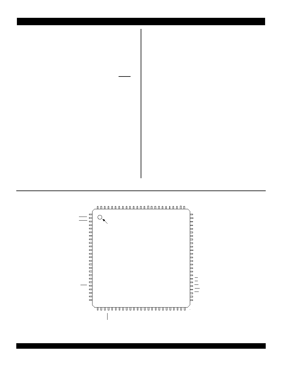
Figure 1 Pin Assignments
1
2
3
4
5
6
7
8
9
10
11
12
13
14
15
16
RXREF
TXREF
TXLED
TXDATA0
TXDATA1
TXDATA2
TXDATA3
TXDATA4
TXDATA5
TXDATA6
TXDATA7
TXEN
TXSOC
VDD
TXCLAV
R
X
A
D
D
R
3
N
C
R
P
L
I
G
N
D
R
X
P
A
R
I
T
Y
R
X
D
A
T
A
7
R
X
D
A
T
A
6
R
X
D
A
T
A
5
R
X
D
A
T
A
4
V
D
D
R
X
D
A
T
A
3
R
X
D
A
T
A
2
R
X
D
A
T
A
1
R
X
D
A
T
A
0
35 36 37
39 40 41 42 43 44 45 46 47 48
50
38
49
51
52
53
54
55
56
57
58
59
60
61
62
63
64
65
66
AD7
AD6
AD5
AD4
GND
AD3
AD2
AD1
AD0
ALE
CS
RD
WR
RST
INT
RXLED
85
86
87
88
89
90
91
92
93
94
95
96
97
98
99
100
S
E
A
G
N
D
A
V
D
D
O
S
C
A
G
N
D
A
V
D
D
A
G
N
D
A
V
D
D
R
X
D
-
R
X
D
+
A
V
D
D
G
N
D
T
X
D
-
T
X
D
+
M
0
5362 drw 02
R
X
A
D
D
R
4
TXPARITY
V
D
D
Pin 1 Index
IDT77V107
17
18
19
20
21
22
23
24
25
TXADDR0
NC
GND
T
X
C
L
K
R
X
E
N
R
X
C
L
A
V
R
X
S
O
C
G
N
D
R
X
A
D
D
R
0
R
X
A
D
D
R
1
R
X
A
D
D
R
2
26 27 28
30 31 32 33 34
29
R
X
C
L
K
67
68
69
70
71
72
73
74
75
76
77
78
79
80
81
82
83
84
VDD
TXADDR1
TXADDR2
TXADDR3
TXADDR4
GND
G
N
D
DA
RCO
VDD
NC
NC
NC
NC
NC
NC
A
G
N
D
V
D
D
M
1
N
C
N
C
N
C
N
C
N
C
N
C
3 of 24
July 3, 2001
IDT77V107
Line Side Signals
Signal Name
Pin Number
I/O
Signal Description
RXD+, RXD-
85, 84
In
Positive and negative receive differential input pair.
TXD+, TXD-
93, 92
Out
Positive and negative transmit differential output pair.
Utility Bus Signals
Signal Name
Pin Number
I/O
Signal Description
AD[7:0]
67, 66, 65, 64,
62, 61, 60, 59
In/Out Utility bus address/data bus. The address input is sampled on the falling edge of ALE. Data is output on this bus when
a read is performed. Input data is sampled at the completion of a write operation.
ALE
58
In
Utility bus address latch enable. Asynchronous input. An address on the AD bus is sampled on the falling edge of ALE.
ALE must be low when the AD bus is being used for data.
CS
57
In
Utility bus asynchronous chip select. CS must be asserted to read or write an internal register. It may remain asserted
at all times if desired.
RD
56
In
Utility bus read enable. Active low asynchronous input. After latching an address, a read is performed by deasserting
WR and asserting RD and CS.
WR
55
In
Utility bus write enable. Active low asynchronous input. After latching an address, a write is performed by deasserting
RD, placing data on the AD bus, and asserting WR and CS. Data is sampled when WR or CS is deasserted.
UTOPIA Bus Signals
Signal Name
Pin Number
I/O
Signal Description
RXADDR[4:0]
37, 36, 35, 34,
33
In
Utopia Receive Address. Address for polling and selecting a Utopia port/PHY.
RXCLAV
30
Out
Utopia Receive Cell Available. "1" indicates that the receive FIFO contains a complete received cell. "0" indicates that
it does not. RXCLAV is high impedance when RXADDR[4:0] does not match the internally programmed Utopia
address.
RXCLK
28
In
Utopia Receive Clock. This is a free running clock input.
RXDATA[7:0]
39, 40, 41, 42,
44, 45, 46, 47
Out
Utopia Receive Data. When one of the four ports is selected, the 77V107 transfers received cells to an ATM device
across this bus. Also see RXPARITY.
RXEN
29
In
Utopia Receive Enable. Driven by an ATM device to indicate its ability to receive data across the RXDATA bus.
RXPARITY
38
Out
Utopia Receive Data Parity. Odd parity over RXDATA[7:0].
RXSOC
31
Out
Utopia Receive Start of Cell. Asserted coincident with the first word of data for each cell on RXDATA.
TXADDR[4:0]
19, 18, 17, 16,
15
In
Utopia Transmit Address. Address for polling and selecting a Utopia port/PHY.
TXCLAV
24
Out
Utopia Transmit Cell Available. "1" indicates that the transmit FIFO has room available for at least one complete cell.
"0" indicates that it does not. TXCLAV is high impedance when TXADDR[4:0] does not match the internally pro-
grammed Utopia address.
TXCLK
27
In
Utopia Transmit Clock. This is a free running clock input.
TXDATA[7:0]
14, 13, 12, 11,
10, 9, 8, 7
In
Utopia Transmit Data. An ATM device transfers cells across this bus to the 77V107 for transmission. Also see TXPAR-
ITY.
TXEN
21
In
Utopia Transmit Enable. Driven by an ATM device to indicate it is transmitting data across the TXDATA bus.
Table 1 Signal Descriptions (Part 1 of 2)

4 of 24
July 3, 2001
IDT77V107
TXPARITY
20
In
Utopia Transmit Data Parity. Odd parity across TXDATA[7:0]. Parity is checked and errors are indicated in the Interrupt
Status Registers, as enabled in the Master Control Register. No other action is taken in the event of an error. Tie high
or low if unused.
TXSOC
22
In
Utopia Transmit Start of Cell. Asserted coincident with the first word of data for each cell on TXDATA.
DA
75
In
Reserved signal. This input must be connected to logic low.
INT
53
Out
Interrupt. INT is an open-drain output, driven low to indicate an interrupt. Once low, INT remains low until the interrupt
status in the appropriate interrupt Status Register is read. Interrupt sources are programmable via the interrupt Mask
Registers.
M1, M0
99, 100
In
Mode Select signals. These inputs must be connected to logic low.
OSC
79
In
TTL line rate clock source, driven by a 100 ppm oscillator. 32 MHz for 25.6 Mbps; 64 MHz for 51.2 Mbps.
RCO
69
Out
Recovered Clock Output. This is the bit clock from the receive section.
RPLI
48
Out
Reserved signal. This output should be allowed to float (unconnected).
RST
54
In
Reset. Active low asynchronous input resets all control logic, counters and FIFOs. A reset must be performed after
power up prior to normal operation of the part.
RXLED
51
Out
Receive LED driver. Driven low for 223 cycles of OSC, beginning with RXSOC when a good (non-null and non-errored)
cell is received. Drives 8 mA both high and low.
RXREF
2
Out
Receive Reference. Active low. RXREF pulses low for a programmable number of clock cycles when an x_8 command
byte is received.
SE
76
In
Reserved signal. This input must be connected to logic low.
TXLED
4
Out
Transmit LED driver. Goes low for 223 cycles of OSC, beginning with TXSOC when a cell is received for transmission.
8 mA drive current both high and low
TXREF
3
In
Transmit Reference. At the falling edge of TXREF, an X_8 command byte is inserted into the transmit data stream.
Typical application is WAN timing.
Power Supply Signals
Signal Name
Pin Number
I/O
Signal Description
AGND
77, 80, 82, 87 ____ Analog ground. AGND is ground the analog portion of the ship, which sources a more constant current than the digital
portion.
AVDD
78, 81, 83, 86 ____
Analog power supply. AVDD supplies power to the analog portion of the chip, which draws a more constant current
than the digital portion. 3.3 ± 0.3V
GND
1, 25, 26, 32,
50, 63, 91
____
Digital Ground.
VDD
6, 23, 43, 68,
94, 98
____
Digital power supply. 3.3 ± 0.3V.
Table 1 Signal Descriptions (Part 2 of 2)
5 of 24
July 3, 2001
IDT77V107
Functional Description
Functional Description
Functional Description
Functional Description
Transmission convergence (TC) sub layer
Transmission convergence (TC) sub layer
Transmission convergence (TC) sub layer
Transmission convergence (TC) sub layer
Introduction
Introduction
Introduction
Introduction
The TC sub layer defines the line coding, scrambling, data framing
and synchronization. Under control of a switch interface or Segmenta-
tion and Reassembly (SAR) unit, the 25.6Mbps ATM PHY accepts a 53-
byte ATM cell, scrambles the data, appends a command byte to the
beginning of the cell, and encodes the entire 53 bytes before transmis-
sion. These data transformations ensure that the signal is evenly distrib-
uted across the frequency spectrum. In addition, the serialized bit
stream is NRZI coded. An 8kHz timing sync pulse may be used for
isochronous communications.
Data Structure and Framing
Data Structure and Framing
Data Structure and Framing
Data Structure and Framing
Each 53-byte ATM cell is preceded with a command byte. This byte
is distinguished by an escape symbol followed by one of 17 encoded
symbols. Together, this byte forms one of seventeen possible command
bytes. Three command bytes are defined:
1. X_X (read: 'escape' symbol followed by another 'escape'): Start-
of-cell with scrambler/descrambler reset.
2. X_4 ('escape' followed by '4'): Start-of-cell without scrambler/
descrambler reset.
3. X_8 ('escape' followed by '8'): 8kHz timing marker. This
command byte is generated when the 8kHz sync pulse is
detected, and has priority over all line activity (data or command
bytes). It is transmitted immediately when the sync pulse is
detected. When this occurs during a cell transmission, the data
transfer is temporarily interrupted on an octet boundary, and the
X_8 command byte is inserted. This condition is the only allowed
interrupt in an otherwise contiguous transfer.
Below is an illustration of the cell structure and command byte usage:
{X_X} {53-byte ATM cell} {X_4} {53-byte ATM {X_8} cell} ...
In the above example, the first ATM cell is preceded by the X_X start-
of-cell command byte which resets both the transmitter-scrambler and
receiver-descrambler pseudo-random nibble generators (PRNG) to their
initial states. The following cell illustrates the insertion of a start-of-cell
command without scrambler/descrambler reset. During this cell's trans-
mission, an 8kHz timing sync pulse triggers insertion of the X_8 8kHz
timing marker command byte.
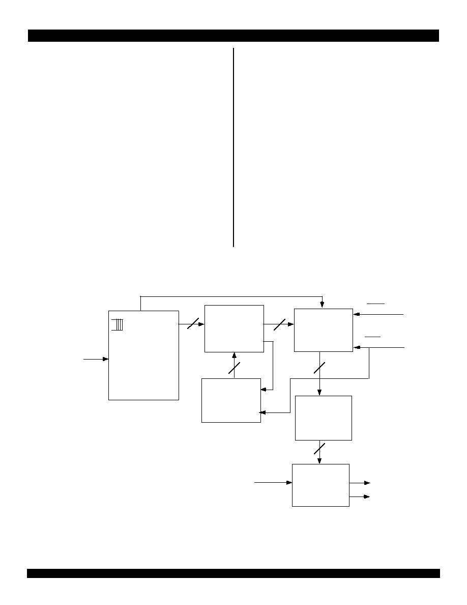
Figure 2
TC Transmit Block Diagram
PHY-ATM
Interface
Control,
HEC Gen. &
Insertion
Scrambler
4
Command
Byte
Insertion
4
PRNG
4
Scramble
Nibble
Next
Reset
4b/5b
Encoding
4
NRZI
Encoding
1
Tx +
Tx -
Line Rate
Clock
TxRef (8kHz)
5362 drw 05
3 Cells
Start of Cell
UTOPIA
Interface
.

6 of 24
July 3, 2001
IDT77V107
Transmission Description
Transmission Description
Transmission Description
Transmission Description
Refer to Figure 4 on the previous page. Cell transmission begins with
the PHY-ATM Interface. An ATM layer device transfers a cell into the
77V107 across the Utopia transmit bus. This cell enters a 3-cell deep
transmit FIFO. Once a complete cell is in the FIFO, transmission begins
by passing the cell, four bits (MSB first) at a time to the 'Scrambler'.
The 'Scrambler' takes each nibble of data and exclusive-ORs them
against the 4 high order bits (X(t), X(t-1), X(t-2), X(t-3)) of a 10 bit
pseudo-random nibble generator (PRNG). Its function is to provide the
appropriate frequency distribution for the signal across the line.
The PRNG is clocked every time a nibble is processed, regardless of
whether the processed nibble is part of a data or command byte. Note
however that only data nibbles are scrambled. The entire command byte
(X _C) is NOT scrambled before it's encoded (see diagram for illustra-
tion). The PRNG is based upon the following polynomial:
X
10
+ X
7
+ 1
With this polynomial, the four output data bits (D3, D2, D1, D0) will
be generated from the following equations:
D3 = d3 xor X(t-3)
D2 = d2 xor X(t-2)
D1 = d1 xor X(t-1)
D0 = d0 xor X(t)
The following nibble is scrambled with X(t+4), X(t+3), X(t+2), and
X(t+1).
A scrambler lock between the transmitter and receiver occurs each
time an X_X command is sent. An X_X command is initiated only at the
beginning of a cell transfer after the PRNG has cycled through all of its
states (2
10
- 1 = 1023 states). The first valid ATM data cell transmitted
after power on will also be accompanied with an X_X command byte.
Each time an X_X command byte is sent, the first nibble after the last
escape (X) nibble is XOR'd with 1111b (PRNG = 3FFx).
Because a timing marker command (X_8) may occur at any time, the
possibility of a reset PRNG start-of-cell command and a timing marker
command occurring consecutively does exist (e.g. X_X_X_8). In this
case, the detection of the last two consecutive escape (X) nibbles will
cause the PRNG to reset to its initial 3FFx state. Therefore, the PRNG is
clocked only after the first nibble of the second consecutive escape pair.
Once the data nibbles have been scrambled using the PRNG, the
nibbles are further encoded using a 4b/5b process. The 4b/5b scheme
ensures that an appropriate number of signal transitions occur on the
line. A total of seventeen 5-bit symbols are used to represent the sixteen
4-bit data nibbles and the one escape (X) nibble. The table below lists
the 4-bit data with their corresponding 5-bit symbols:
This encode/decode implementation has several very desirable
properties. Among them is the fact that the output data bits can be
represented by a set of relatively simple symbols;
!
Run length is limited to <= 5;
!
Disparity never exceeds +/- 1.
On the receiver, the decoder determines from the received symbols
whether a timing marker command (X_8) or a start-of-cell command
was sent (X_X or X_4). If a start-of-cell command is detected, the next
53 bytes received are decoded and forwarded to the descrambler. (See
the TC Receive Block Diagram).
The output of the 4b/5b encoder provides serial data to the NRZI
encoder. The NRZI code transitions the wire voltage each time a '1' bit is
sent. This, together with the previous encoding schemes guarantees
that long run lengths of either '0' or '1's are prevented. Each symbol is
shifted out with its most significant bit sent first.
When no cells are available to transmit, the 77V107 keeps the line
active by continuing to transmit valid symbols. But it does not transmit
another start-of-cell command until it has another cell for transmission.
The 77V107 never creates its own idle cells for transmission.
Transmit HEC Byte Calculation/Insertion
Transmit HEC Byte Calculation/Insertion
Transmit HEC Byte Calculation/Insertion
Transmit HEC Byte Calculation/Insertion
Byte #5 of each ATM cell, the HEC (Header Error Control) is calcu-
lated automatically across the first 4 bytes of the cell header, depending
upon the setting of bit 5 of the LED Driver and HEC Status/Control
Register (0x03). This byte is then either inserted as a replacement of the
fifth byte transferred to the PHY by the external system, or the cell is
transmitted as received. A third operating mode provides for insertion of
"Bad" HEC codes which may aid in communication diagnostics. These
modes are controlled by the LED Driver and HEC Status/Control Regis-
ters.
Receiver Description
Receiver Description
Receiver Description
Receiver Description
The receiver side of the TC sublayer operates like the transmitter,
but in reverse. The data is NRZI decoded before each symbol is reas-
sembled. The symbols are then sent to the 5b/4b decoder, followed by
the Command Byte Interpreter, De-Scrambler, and finally through a
FIFO to the UTOPIA interface to an ATM Layer device.
Data
0000
0100
1000
1100
Symbol
10101
00111
10010
10111
Symbol
01001
01101
11001
11101
Data
0001
0101
1001
1101
Symbol
01010
01110
11010
11110
Data
0010
0110
1010
1110
Data
0011
0111
1011
1111
ESC(X) = 00010
3505 drw 05a
Symbol
01011
01111
11011
11111
.
.
7 of 24
July 3, 2001
IDT77V107
Figure 3 ATM Cell Format
Note that although the IDT77V107 can detect symbol and HEC
errors, it does not attempt to correct them.
Upon resetting the device or re-establishing a serial link, logic in front
of the 4b/5b decoder uses feedback from the 4b/5b decoder to deter-
mine if it is not properly "framed" on the 5-bit symbols. If not properly
Bit 7
Bit 0
Header Byte 1
Header Byte 2
Header Byte 3
Header Byte 4
UDF
Payload Byte 1
∑
∑
∑
Payload Byte 48
3505 drw 52
UDF = User Defined Field (or HEC)
.
framed, it will shift its framing, one bit at a time, until it achieves proper
symbol framing. Receipt of an Escape (X) symbol will also force proper
symbol framing.
The IDT77V107 monitors line conditions and can provide an interrupt
if the line is deemed 'bad'. The Interrupt Status Register contains a
Good Signal Bit (bit 6, set to 0 = Bad signal initially) which shows the
status of the line per the following algorithm:
To declare 'Good Signal' (from "Bad" to "Good"):
To declare 'Good Signal' (from "Bad" to "Good"):
To declare 'Good Signal' (from "Bad" to "Good"):
To declare 'Good Signal' (from "Bad" to "Good"):
There is an up-down counter that counts from 7 to 0 and is initially
set to 7. When the clock ticks for 1,024 cycles (32MHz clock, 1,024
cycles = 204.8 symbols) and no "bad symbol" has been received, the
counter decreases by one. However, if at least one "bad symbol" is
detected during these 1,024 clocks, the counter is increased by one, to a
maximum of 7. The Good Signal Bit is set to 1 when this counter
reaches 0. The Good Signal Bit could be set to 1 as quickly as 1,433
symbols (204.8 x 7) if no bad symbols have been received.
Figure 4 TC Receive Block Diagram
4
PHY-ATM
Interface
Control -
RECV
4
5
NRZI
Decoding
Rx +
Rx
4
4
PRNG
Scramble
Nibble
Next
Reset
RxRef
Line Clock
Synthesizer
& PLL
5b/4b
Decoding
Command
Byte
Detection,
Removal,
& Decode
De-
Scrambler
5362 drw 06
OSC
3 Cells
Start of Cell
UTOPIA
Interface
.

8 of 24
July 3, 2001
IDT77V107
To declare 'Bad Signal' (from "Good" to "Bad"):
To declare 'Bad Signal' (from "Good" to "Bad"):
To declare 'Bad Signal' (from "Good" to "Bad"):
To declare 'Bad Signal' (from "Good" to "Bad"):
The same up-down counter counts from 0 to 7 (being at 0 to provide
a "Good" status). When the clock ticks for 1,024 cycles (32MHz clock,
1,024 cycles = 204.8 symbols) and there is at least one "bad symbol",
the counter increases by one. If it detects all "good symbols" and no
"bad symbols" in the next time period, the counter decreases by one.
The "Bad Signal" is declared when the counter reaches 7. The Good
Signal Bit could be set to 0 as quickly as 1,433 symbols (204.8 x 7) if at
least one "bad symbol" is detected in each of seven consecutive groups
of 204.8 symbols.
8kHz Timing Marker
8kHz Timing Marker
8kHz Timing Marker
8kHz Timing Marker
The 8kHz timing marker, described earlier, is a completely optional
feature which is essential for some applications requiring synchroniza-
tion for voice or video, and unnecessary for other applications. When
unused, TXREF should be tied high. Also note that it is not limited to
8kHz, should a different frequency be desired. When looped, a received
X_8 command byte causes one to be generated on the transmit side.
A received X_8 command byte causes the 77V107 to issue a nega-
tive pulse on RXREF. The source channel of the marker is program-
mable.
Utopia Level 2 PHY-ATM Interface
Utopia Level 2 PHY-ATM Interface
Utopia Level 2 PHY-ATM Interface
Utopia Level 2 PHY-ATM Interface
UTOPIA Level 2 is a Physical Layer to ATM Layer interface standard-
ized by the ATM Forum. It is selected using the M1 and M0 pins. It trans-
fers ATM cells and has separate transmit and receive channels and
specific handshaking protocols. UTOPIA Level 2 has dedicated address
signals for both the transmit and receive directions that allow the ATM
layer device to specify which PHY device it is communicating with. It is
defined in ATM Forum document af-phy-0039.
Note that the 77V107 supports the standard "Operation with 1
TxClav and 1 Rx Clav" multi-phy scheme from the Utopia Level 2 stan-
dard. The optional Multiplexed Status Polling multi-phy scheme is not
directly supported.
There is a single 8-bit data bus in the transmit (ATM-to-PHY) direc-
tion, and a single 8-bit data bus in the receive (PHY-to-ATM) direction. In
addition to the data bus, each direction also includes a single optional
parity bit, an address bus, and several handshaking signals. The
UTOPIA address of the PHY is determined by bits 4 to 0 in the
Enhanced Control Register. Please note that the transmit bus and the
receive bus operate completely independently. The Utopia signals are
summarized below:
The ATM device starts by polling the PHY ports on the Utopia bus to
determine if any of them has room to accept a cell for transmission
(TXCLAV), or has a receive cell available to pass on to the ATM device
(RXCLAV). To poll, the ATM device drives an address (TXADDR or
RXADDR) then observes TXCLAV or RXCLAV on the next cycle of
TXCLK or RXCLK. The PHY will tri-state TXCLAV and RXCLAV except
when it is addressed.
If TXCLAV or RXCLAV is asserted, the ATM device may select the
PHY, then transfer a cell to or from it. Selection of a PHYis performed by
driving the address of the desired port while TXEN or RXEN is high,
then driving TXEN or RXEN low. When TXEN is driven low, TXSOC
(start of cell) is driven high to indicate that the first byte of the cell
isbeing driven on TXDATA. The ATM device may chose to temporarily
suspend transfer of the cell by deasserting TXEN. Otherwise, TXEN
remains asserted as the next byte is driven onto TXDATA with each
cycle of TXCLK.
In the receive direction, the ATM device selects a PHY if it wishes to
receive the cell that the PHY is holding. It does this by asserting RXEN.
The PHY then transfers the data 8 bits each clock cycle, as determined
by RXEN. As in the transmit direction, the ATM device may suspend
transfer by deasserting RXEN at any time. Note that the PHY asserts
RXSOC coincident with the first byte of each cell.
TXPARITY and RXPARITY are parity bits for the corresponding 8-bit
data fields. Odd parity is used, which means that for an all-zero data
pattern, the corresponding parity bit is one.
The following figures may be referenced for Utopia Level 2 bus
examples.
TXDATA[7:0]
ATM to PHY
TXPARITY
ATM to PHY
TXSOC
ATM to PHY
TXADDR[4:0]
ATM to PHY
TXEN
ATM to PHY
TXCLAV
PHY to ATM
TXCLK
ATM to PHY
RXDATA[7:0]
PHY to ATM
RXPARITY
PHY to ATM
RXSOC
PHY to ATM
RXADDR[4:0]
ATM to PHY
RXEN
ATM to PHY
RXCLAV
PHY to ATM
RXCLK
ATM to PHY

9 of 24
July 3, 2001
IDT77V107
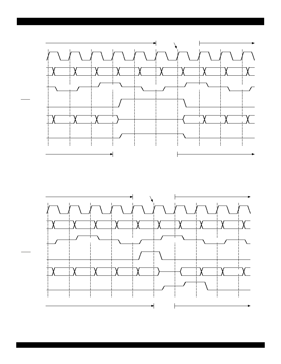
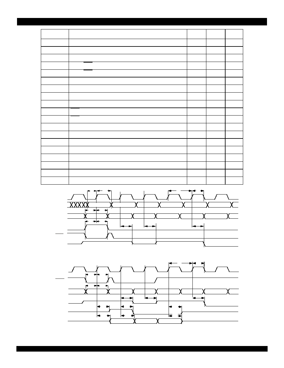
Figure 5 Utopia Transmit Handshake - Back to Back Cells
Figure 6 Utopia Transmit Handshake - Delay Between Cells
TxCLK
TxSOC
TxCLAV
TxEN
TxData[7:0],
TxPARITY
P44
P45
P46
P47
P48
H1
H2
H3
77v1054 drw 09
TxADDR[4:0]
1F
N+3
1F
N+2
1F
N+3
1F
N
1F
N+3
N+2
N+3
N
N+1
PHY N
PHY N+3
cell transmission to:
polling
polling
polling:
selection
H4
High-Z
.
TxCLK
TxSOC
TxCLAV
TxEN
TxData[7:0],
TxPARITY
P46
P47
P48
H1
H2
H3
77v1054 drw 10
TxADDR[4:0]
1F
N+3
1F
N+2
1F
N+3
1F
N
1F
N+3
N+2
N+3
N
N+1
PHY N
PHY N+3
cell transmission to:
polling
polling
polling:
selection
H4
High-Z
.
10 of 24
July 3, 2001
IDT77V107
Figure 7 Utopia Transmit Handshake - Transmission Suspended
Figure 8 Utopia Receive Handshake - Back to Back Cells
TxCLK
TxSOC
TxCLAV
TxEN
TxData[7:0],
TxPARITY
P28
P29
P30
P31
P32
77v1054 drw 11
TxADDR[4:0]
1F
N+3
1F
N+2
1F
M
1F
N
1F
N+3
N+2
M
N
N+1
PHY M
PHY M
cell transmission to:
polling
polling
polling:
selection
P33
High-Z
High-Z
High-Z
.
RxCLK
RxSOC
RxCLAV
RxEN
RxData[7:0],
RxPARITY
P44
P45
P46
P47
P48
H1
H2
H3
77v1054 drw 12
RxADDR[4:0]
1F
N+3
1F
N+2
1F
N+3
1F
N
1F
N+3
N+2
N+3
N
N+1
PHY N
PHY N+3
cell transmission to:
polling
polling
polling:
selection
H4
High-Z
High-Z
High-Z
.
11 of 24
July 3, 2001
IDT77V107
Figure 9 Utopia Receive Handshake - Delay Between Cells
Figure 10 Utopia 2 Receive Handshake - Suspended Transfer of Data
RxCLK
RxSOC
RxCLAV
RxEN
RxData[7:0],
RxPARITY
P47
P48
H1
H2
77v1054 drw 13
RxADDR[4:0]
N+3
1F
N+2
1F
N+1
1F
N+1
1F
N+3
N+2
N+1
N+1
N
PHY N+3
PHY N+1
cell transmission to:
polling
polling
polling:
selection
undefined
1F
High-Z
High-Z
High-Z
.
RxCLK
RxSOC
RxCLAV
RxEN
RxData[7:0],
RxPARITY
P28
P29
P30
P31
P32
77v1054 drw 14
RxADDR[4:0]
N+3
1F
N+2
1F
M
1F
N+1
1F
N+3
N+2
M
N+1
PHY M
PHY M
cell transmission from:
polling
polling
polling:
re-selection
P33
N+2
High-Z
High-Z
High-Z
.

12 of 24
July 3, 2001
IDT77V107
Control and Status Interface
Control and Status Interface
Control and Status Interface
Control and Status Interface
Utility Bus
Utility Bus
Utility Bus
Utility Bus
The Utility Bus is a byte-wide interface that provides access to the
registers within the IDT77V107. These registers are used to select
desired operating characteristics and functions, and to communicate
status to external systems.
The Utility Bus is implemented using a multiplexed address and data
bus (AD[7:0]) where the register address is latched via the Address
Latch Enable (ALE) signal.
The Utility Bus interface is comprised of the following pins:
AD[7:0], ALE, CS, RD, WR
Read Operation
Read Operation
Read Operation
Read Operation
Refer to the Utility Bus timing waveforms. A register read is
performed as follows:
1. Initial condition:
≠ RD, WR, CS not asserted (logic 1)
≠ ALE not asserted (logic 0)
2. Set up register address:
≠ place desired register address on AD[7:0]
≠ set ALE to logic 1;
≠ latch this address by setting ALE to logic 0.
3. Read register data:
≠ Remove register address data from AD[7:0]
≠ assert CS by setting to logic 0;
≠ assert RD by setting to logic 0
≠ wait minimum pulse width time (see AC specifications)
Write Operation
Write Operation
Write Operation
Write Operation
A register write is performed as described below:
1. Initial condition:
≠ RD, WR, CS not asserted (logic 1)
≠ ALE not asserted (logic 0)
2. Set up register address:
≠ place desired register address on AD[7:0]
≠ set ALE to logic 1;
≠ latch this address by setting ALE to logic 0.
3. Write data:
≠ place data on AD[7:0]
≠ assert CS by setting to logic 0;
≠ assert WR (logic 0) for minimum time (according to timing
specification); reset WR or CS to logic 1 to complete register
write cycle.
Interrupt Operations
Interrupt Operations
Interrupt Operations
Interrupt Operations
A variety of selectable interrupt and signalling conditions are
provided. They are useful both during `normal' operation, and as diag-
nostic aids. Refer to the Status and Control Register List section.
Overall interrupt control is provided via bit 0 of the Master Control
Register. When this bit is cleared (set to 0), interrupt signalling is
prevented on the respective port. The Interrupt Mask Register allows
individual masking of different interrupt sources. Additional interrupt
signal control is provided by bit 5 of the Master Control Register. When
this bit is set (=1), receive cell errors will be flagged via interrupt signal-
ling and all other interrupt conditions are masked. These errors include:
≠ Bad receive HEC
≠ Short (fewer than 53 bytes) cells
≠ Received cell symbol error
Normal interrupt operations are performed by setting bit 0 and
clearing bit 5 in the Master Control Register. INT (pin 34) will go to a low
state when an interrupt condition is detected. The external system
should then interrogate the 77V107 to determine which one (or more)
conditions caused this flag, and reset the interrupt for further occur-
rences. This is accomplished by reading the Interrupt Status Register.
Decoding the bits in this byte will tell which error condition caused the
interrupt. Reading these registers also:
≠ clears the (sticky) interrupt status bits in the registers that are
read
≠ resets INT
This leaves the interrupt system ready to signal an alarm for further
problems.
LED Control and Signalling
LED Control and Signalling
LED Control and Signalling
LED Control and Signalling
The LED outputs provide bi-directional LED drive capability of 8 mA.
As an example, the RxLED outputs are described in the truth table:
As illustrated in the following figure, this could be connected to
provide for a two-LED condition indicator. These could also be different
colors to provide simple status indication at a glance. (The minimum
value for R should be 330
).
TxLED Truth Table
TxLED Truth Table
TxLED Truth Table
TxLED Truth Table
Figure 11
State
Pin Voltage
Cells being transmitted
Low
Cells not being received
High
State
Pin Voltage
Cells being transmitted
Low
Cells not being received
High
RxLED
TxLED
3.3V
(Indicates: Cells
being received or
transmitted)
(Indicates: Cells are
not being received or
transmitted)
5362 drw 32
R
R
13 of 24
July 3, 2001
IDT77V107
Diagnostic Functions
Diagnostic Functions
Diagnostic Functions
Diagnostic Functions
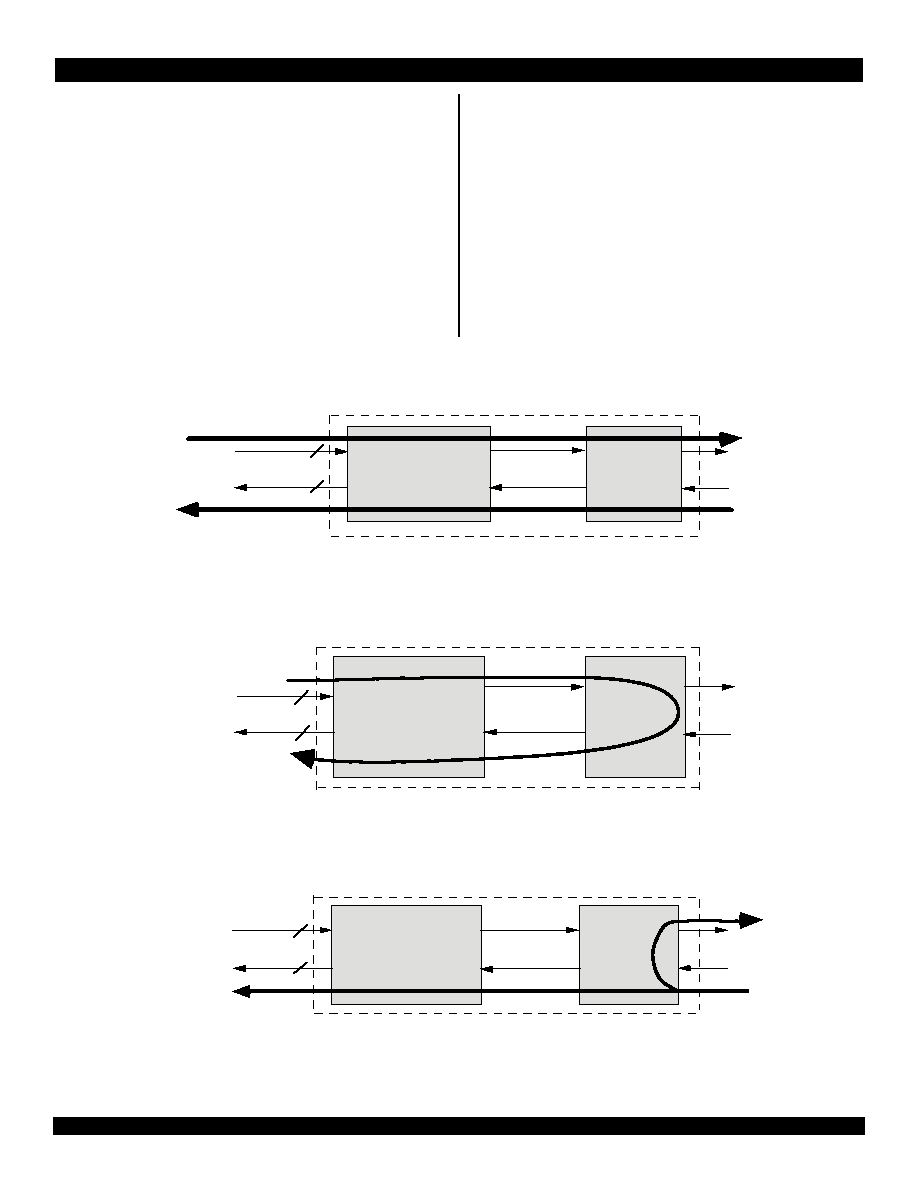
1. Loopback
1. Loopback
1. Loopback
1. Loopback
There are two loopback modes supported by the 77V107. The loop-
back mode is controlled via bits 1 and 0 of the Diagnostic Control Regis-
ters:
Normal Mode
Normal Mode
Normal Mode
Normal Mode
Figure 12 shows normal operating conditions: data to be transmitted
is transferred to the TC, where it is queued and formatted for transmis-
sion by the PMD. Receive data from the PMD is decoded along with its
clock for transfer to the receiving "upstream system".
PHY Loopback
PHY Loopback
PHY Loopback
PHY Loopback
As Figure 13 illustrates below, this loopback mode provides a
connection within the PHY from the transmit PHY-ATM interface to the
PHY-ATM receive interface. Note that while this mode is operating, no
data is forwarded to or received from the line interface.
Line Loopback
Line Loopback
Line Loopback
Line Loopback
Figure 14 might also be called "remote loopback" since it provides for
a means to test the overall system, including the line. Since this mode
will probably be entered under direction from another system (at a
remote location), receive data is also decoded and transferred to the
upstream system to allow it to listen for commands. A common example
would be a command asking the upstream system to direct the TC to
leave this loopback state, and resume normal operations.
Figure 12 Normal Mode
Figure 13 PHY Loopback
Figure 14 Line Loopback
TC sublayer
PMD sublayer
Line
Interface
ATM Layer
Device
5362 drw 33
Utopia
Interface
ATM Layer
Device
TC sublayer
PMD sublayer
Line
Interface
77v1054 drw 34
Utopia
Interface
ATM Layer
Device
TC sublayer
PMD
sublayer
Line
Interface
77v1054 drw 35
Utopia
Interface

14 of 24
July 3, 2001
IDT77V107
2. Counters
2. Counters
2. Counters
2. Counters
Several condition counters are provided to assist external systems
(e.g. software drivers) in evaluating communications conditions. It is
anticipated that these counters will be polled from time to time (user
selectable) to evaluate performance.
!
Symbol Error Counters
≠ 8 bits
≠ counts all invalid 5-bit symbols received
!
Transmit Cell Counters
≠ - 16 bits
≠ counts all transmitted cells
!
Receive Cell Counters
≠ - 16 bits
≠ counts all received cells, excluding idle cells and HEC errored
cells
!
Receive HEC Error Counters
≠ 5 bits
≠ counts all HEC errors received
The TxCell and RxCell counters are sized (16 bits) to provide a full
cell count (without roll over) if the counter is read once/second. The
Symbol Error counter and HEC Error counter were given sufficient size
to indicate exact counts for low error-rate conditions. If these counters
overflow, a gross condition is occurring, where additional counter resolu-
tion does not provide additional diagnostic benefit.
Reading Counters
Reading Counters
Reading Counters
Reading Counters
1. Decide which counter value is desired. Write to the Counter
Select Register to the bit location corresponding to the desired
counter. This loads the High and Low Byte Counter Registers with
the selected counter's value, and resets this counter to zero.
NOTE: Only one counter may be enabled at any time in the
Counter Select Register.
2. Read the Counter Registers (low byte and high byte) to get the
value.
Further reads may be accomplished in the same manner by writing to
the Counter Select Registers.
Line Side (Serial) Interfac
Line Side (Serial) Interfac
Line Side (Serial) Interfac
Line Side (Serial) Interfaceeee
P
P
P
PHY to Magnetics Interface
HY to Magnetics Interface
HY to Magnetics Interface
HY to Magnetics Interface
A standard connection to 100
and 120
unshielded twisted pair
cabling is shown in the figure below. Note that the transmit signal is
somewhat attenuated in order to meet the launch amplitude specified by
the standards. The receive circuitry is designed to attenuate low
frequencies in order to compensate for the high frequency attenuation of
the cable.
Also, the receive circuitry biases the positive and negative RX inputs
to slightly different voltages. This is done so that the receiver does not
receive false signals in the absence of a real signal. This can be impor-
tant because the 77V107 does not disable error detection or interrupts
when an input signal is not present.
When connecting to UTP at 51.2 Mbps, it is necessary to use
magnetics with sufficient bandwidth. Such a device can also operate
satisfactorily at 25.6 Mbps.
Figure 15 Recommended Connection to Magnetics
7
8
10
9
3
4
5
Magnetics
R
J
4
5
C
o
n
n
e
c
t
o
r
IDT77V107
AGND
14
13
12
AGND
1
2
16
15
AGND
AVDD
RxD+
RxD-
TxD+
TxD-
R1
R2
R3
R4
R6
R8
R9
R10
C1
C2
L1
5362 drw 36
R7
1
2
3
4
5
6
7
8
.
R5
C3

15 of 24
July 3, 2001
IDT77V107
Component
Value
Tolerance
R1
47
±5%
R2
47
±5%
R3
620
±5%
R4
62
±5%
R5
62
±5%
R6
10k
±5%
R7
10k
±5%
R8
33
±5%
R9
33
±5%
R10
82
±5%
C1
470pF
±20%
C2
470pF
±20%
C3
0.1
µ
F
±20%
L1
3.3
µ
H
±20%
Table 2 Analog Component Values
Magnetics Modules for 25.6 Mbps
Magnetics Modules for 25.6 Mbps
Magnetics Modules for 25.6 Mbps
Magnetics Modules for 25.6 Mbps
Magnetics Modules for 51.2 Mbps
Magnetics Modules for 51.2 Mbps
Magnetics Modules for 51.2 Mbps
Magnetics Modules for 51.2 Mbps
Status and Control Register List
Status and Control Register List
Status and Control Register List
Status and Control Register List
Nomenclature
Nomenclature
Nomenclature
Nomenclature
"Reserved" register bits, if written, should always be written "0"
R/W = register may be read and written via the utility bus
R-only or W-only = register is read-only or write-only
sticky = register bit is cleared after the register containing it is read;
all sticky bits are read-only
"0" = `cleared' or `not set'
"1" = `set'
Pulse PE-67583 or R4005
(619) 674-8100
TDK TLA-6M103
(847) 803-6100
Pulse R4005
(619) 674-8100
Master Control Register
Master Control Register
Master Control Register
Master Control Register
Address:0x00
Address:0x00
Address:0x00
Address:0x00
Bit Type
Initial State
Function
7
R/W
0 = OSC
multiplied by one
Clock Multiplier Controls whether or not the OSC reference clock input is multiplied by two to generate the line
clock.
Cleared (0) = OSC is multiplied by 1 to generate line clock
Set (1) = OSC is multiplied by 2 to generate line clock
6
R/W
1 = discard errored
cells
Discard Receive Error Cells On receipt of any cell with an error (e.g. short cell, invalid command mnemonic,
receive HEC error (if enabled)), this cell will be discarded and will not enter the receive FIFO.
5
R/W
0 = all interrupts
Enable Cell Error Interrupts Only If Bit 0 in this register is set (Interrupts Enabled), setting of this bit enables only
"Received Cell Error" (as defined in bit 6) to trigger interrupt line.
4
R/W
0 = disabled
Transmit Data Parity Check Directs TC to check parity of TxDATA against parity bit located in TXPARITY.
3
R/W
1= discard idle cells
Discard Received Idle Cells Directs TC to discard received idle (VPI/VCI = 0 and GFC = 0) cells from PMD without
signalling external systems.
2
R/W
0 = not halted
Halt Tx Halts transmission of data from TC to PMD and forces the TxD outputs to the "0" state.
1
R/W
0
Reserved
0
R/W
1 = enable interrupts
Enable Interrupt Pin (Interrupt Mask Bit) Enables the INT output pin. If cleared, pin is always high and interrupt is
masked. If set, an interrupt will be signaled by setting the interrupt pin to "0". It doesn't affect the Interrupt Status Reg-
isters.

16 of 24
July 3, 2001
IDT77V107
Interrupt Status Register
Interrupt Status Register
Interrupt Status Register
Interrupt Status Register
Address:0x01
Address:0x01
Address:0x01
Address:0x01
Diagnostic Control Register
Diagnostic Control Register
Diagnostic Control Register
Diagnostic Control Register
Address:0x02
Address:0x02
Address:0x02
Address:0x02
Bit Type Initial State
Function
7
0
Reserved
6
R
0 = Bad Signal
Good Signal Bit See definitions earlier in this data sheet.
1 - Good Signal
0 - Bad Signal
5
sticky
0
HEC error cell received Set when a HEC error is detected on received cell.
4
sticky
0
"Short Cell" Received Interrupt signal which flags received cells with fewer than 53 bytes. This condition is detected
when receiving Start-of-Cell command bytes with fewer than 53 bytes between them.
3
sticky
0
Transmit Parity Error If Bit 4 of the Master Control Register (Transmit Data Parity Check) is set, this interrupt flags a
transmit data parity error condition. Odd parity is used.
2
sticky
0
Receive Signal Condition change This interrupt is set when the received 'signal' changes either from 'bad to good' or
from 'good to bad'.
1
sticky
0
Received Symbol Error Set when an undefined 5-bit symbol is received.
0
sticky
0
Receive FIFO Overflow Interrupt which indicates when the receive FIFO has filled and cannot accept additional data.
Bit Type Initial State
Function
7
R/W
0 = normal
Force TxCLAV Deassert This feature can be used during line loopback mode to prevent cells from being passed
across the Utopia bus for transmission.
6
R/W
0
Reserved
5
R/W
1
Reserved
4
R/W
0 = normal
RFLUSH = Clear Receive FIFO This signal is used to tell the TC to flush (clear) all data in the receive FIFO. The TC
signals this completion by clearing this bit.
3
R/W
0 = normal
Insert Transmit Payload Error Tells TC to insert cell payload errors in transmitted cells. This can be used to test error
detection and recovery systems at destination station, or, under loopback control, at the local receiving station. This pay-
load error is accomplished by flipping bit 0 of the last cell payload byte.
2
R/W
0 = normal
Insert Transmit HEC Error Tells TC to insert HEC error in Byte 5 of transmitted cells. This can be used to test error
detection and recovery systems in downstream switches, or, under loopback control, the local receiving station. The HEC
error is accomplished by flipping bit 0 of the HEC byte.
1, 0
R/W
00 = normal
Loopback Control
bit # 1 0
0 0 Normal mode (receive from network)
1 0 PHY Loopback
1 1 Line Loopback

17 of 24
July 3, 2001
IDT77V107
LED Driver and HEC Status/Control Registers
LED Driver and HEC Status/Control Registers
LED Driver and HEC Status/Control Registers
LED Driver and HEC Status/Control Registers
Address:0x03
Address:0x03
Address:0x03
Address:0x03
Low Byte Counter Register [7:0]
Low Byte Counter Register [7:0]
Low Byte Counter Register [7:0]
Low Byte Counter Register [7:0]
Address:0x04
Address:0x04
Address:0x04
Address:0x04
High Byte Counter Register [15:8]
High Byte Counter Register [15:8]
High Byte Counter Register [15:8]
High Byte Counter Register [15:8]
Address:0x05
Address:0x05
Address:0x05
Address:0x05
Counter Select Register
Counter Select Register
Counter Select Register
Counter Select Register
Address:0x06
Address:0x06
Address:0x06
Address:0x06
Note: For proper operation, only one bit may be set in the Counter Select Register at any time.
Bit Type
Initial State
Function
7
R
0
Reserved
6
R/W
0 = enable checking
Disable Receive HEC Checking (HEC Enable) When not set, the HEC is calculated on first 4 bytes of received
cell, and compared against the 5th byte. When set (= 1), the HEC byte is not checked.
5
R/W
0 = enable calculate &
replace
Disable Transmit HEC Calculate & Replace When set, the 5th header byte of cells queued for transmit is not
replaced with the HEC calculated across the first four bytes of that cell.
4,3
R/W
00 = 1 cycle
RxREF Pulse Width Select
bit # 4 3
0 0 RxREF active for 1 cycle of the recovered clock
0 1 RxREF active for 2 cycles of the recovered clock
1 0 RxREF active for 4 cycles of the recovered clock
1 1 RxREF active for 8 cycles of the recovered clock
2
R
1 = empty
Transmit FIFO Status 1 = TxFIFO empty 0 = TxFIFO not empty
1
R
1
TxLED Status 0 = Cell Transmitted 1 = Cell Not Transmitted
0
R
1
RxLED Status 0 = Cell Received 1 = Cell Not Received
Bit Type Initial State
Function
[7:0] R
0x00
Provides low-byte of counter value selected via the Counter Select Register.
Bit Type Initial State
Function
[7:0] R
0x00
Provides high-byte of counter value selected via the Counter Select Register.
Bit Type Initial State
Function
7
--
0
Reserved
6
--
0
Reserved
5
--
0
Reserved
4
--
0
Reserved
3
W
0
Symbol Error Counter
2
W
0
TxCell Counter
1
W
0
RxCell Counter Does not count HEC errored cells, even when bit 6 of the Master Control Register is cleared.
0
W
0
Receive HEC Error Counter

18 of 24
July 3, 2001
IDT77V107
Interrupt Mask Register
Interrupt Mask Register
Interrupt Mask Register
Interrupt Mask Register
Address:0x07
Address:0x07
Address:0x07
Address:0x07
Note: When set to "1", these bits mask the corresponding interrupts going to the interrupt pin (INT). When set to "0", the interrupts are
unmasked. These interrupts correspond to the interrupt status bits in the Interrupt Status Registers.
Enhanced Control Register
Enhanced Control Register
Enhanced Control Register
Enhanced Control Register
Address:0x08
Address:0x08
Address:0x08
Address:0x08
Absolute Maximum Ratings Recommended DC Operating Conditions
Absolute Maximum Ratings Recommended DC Operating Conditions
Absolute Maximum Ratings Recommended DC Operating Conditions
Absolute Maximum Ratings Recommended DC Operating Conditions
Bit Type
Initial State
Function
7
0
Reserved
6
0
Reserved
5
R/W
0 = interrupt enabled
HEC Error Cell.
4
R/W
0 = interrupt enabled
Short Cell Error.
3
R/W
0 = interrupt enabled
Transmit Parity Error.
2
R/W
0 = interrupt enabled
Receive Signal Condition Change.
1
R/W
0 = interrupt enabled
Received Cell Symbol Error.
0
R/W
0 = interrupt enabled
Receive FIFO Overflow.
Bit Type Initial State
Function
7
W
0 = not reset
Software Reset 1 = Reset. This bit is self-clearing; it isn't necessary to write ""0"" to exit reset.
6
R/W
0 = OSC
Transmit Line Clock (or Loop Timing Mode) When set to 0, the OSC input is used as the transmit line clock. When
set to 1, the recovered receive clock is used as the transmit line clock.
5
R/W
0
Reserved
4-0
R/W
00000
Utopia Port Address These bits determine the 5-bit address of the Utopia port for both receive and transmit.
Symbol
Rating
Value
Unit
Symbol
Parameter
Min
Typ
Max
Unit
V
TERM
Terminal Voltage with
Respect to GND
-0.5 to +5.5 V
VDD
Digital Supply Voltage
3.0
3.3
3.6
V
GND
Digital Ground Voltage
0
0
0
V
T
BIAS
Temperature Under Bias -55 to +125
∞
C
VIH
Input High Voltage
2.0
____
5.25
V
T
STG
Storage Temperature
-55 to +120
∞
C
VIL
Input Low Voltage
-0.3
____
0.8
V
I
OUT
DC Output Current
50
mA
AVDD
Analog Supply Voltage
3.0
3.3
3.6
V
Note: Stresses greater than those listed under ABSOLUTE MAXIMUM
RATINGS may cause permanent damage to the device. This is a stress
rating only and functional operation of the device at these or any other
conditions above those indicated in the operational sections of this
specification is not implied. Exposure to absolute maximum rating condi-
tions for extended periods may affect reliabilty.
AGND
Analog Ground Voltage
0
0
0
V
VDIF
VDD - AVDD
-0.5
0
0.5
V
19 of 24
July 3, 2001
IDT77V107
Recommended Operating
Recommended Operating
Recommended Operating
Recommended Operating
C
C
C
Capacitance
apacitance
apacitance
apacitance
Temperature and Supply Voltage
Temperature and Supply Voltage
Temperature and Supply Voltage
Temperature and Supply Voltage
(
(
(
(TA = +25
TA = +25
TA = +25
TA = +25
∞
∞
∞
∞
C,
C,
C,
C, f =
f =
f =
f = 1MHz)
1MHz)
1MHz)
1MHz)
DC Electrical Characteristics (All Pins except TXD+/- and RXD+/-)
DC Electrical Characteristics (All Pins except TXD+/- and RXD+/-)
DC Electrical Characteristics (All Pins except TXD+/- and RXD+/-)
DC Electrical Characteristics (All Pins except TXD+/- and RXD+/-)
DC Electrical Characteristics
DC Electrical Characteristics
DC Electrical Characteristics
DC Electrical Characteristics (TXD+/- Output Pins Only)
DC Electrical Characteristics
DC Electrical Characteristics
DC Electrical Characteristics
DC Electrical Characteristics (RXD+/- Input Pins Only)
UTOPIA Bus Timing Prameters
UTOPIA Bus Timing Prameters
UTOPIA Bus Timing Prameters
UTOPIA Bus Timing Prameters
Grade
Ambiant
Temperature
GND,
AGND
VDD,
AVDD
Symbol
Parameter
Conditions
Max Unit
Commercial 0
∞
C to +70
∞
C
0V
3.3V ± 0.3V
C
IN1
Input Capacitance
VIN = 0V
10
pF
Industrial
-40
∞
C to +85
∞
C
0V
3.3V ± 0.3V
C
IO1
I/O Capacitance
VOUT = 0V
10
pF
1.
Characterized values, not currently tested.
Symbol
Parameter
Test Conditions
Min
Max
Unit
I
LI
Input Leakage Current (TxADDR, RxADDR, M0, DA)
Gnd
VIN
VDD
-60
60
µA
Input Leakage Current (all other input signals)
Gnd
VIN
VDD
-5
5
µA
V
OH11
1.
For AD[7:0] pins only.
Output Logic "1" Voltage
IOH = -2mA, VDD = min.
2.4
___
V
V
OH22
2.
For all output pins except AD[7:0], INT and TXD+/-.
Output Logic "1" Voltage
IOH = -8mA, VDD = min.
2.4
___
V
V
OL3
3.
For all output pins except TXD+/-.
Output Logic "0" Voltage
IOL = 8mA, VDD = min.
___
0.4
V
I
DD14
,
5
4.
Add 15mA when TXD+/- are driving a load
5.
Total supply current is the sum of IDD1 and IDD2
Digital Power Supply Current (VDD pins)
OSC = 32 MHz, all outputs unloaded
___
45
mA
OSC = 64 MHz, all outputs unloaded
___
80
mA
I
DD2
5
Analog Power Supply Current (AVDD pins)
OSC = 32 MHz, all outputs unloaded
___
40
mA
OSC = 64 MHz, all outputs unloaded
___
55
mA
Symbol
Parameter
Test Conditions
Min
Max
Unit
VOH
Output Logic High Voltage
IOH = -20mA
VDD - 0.5V
____
V
VOL
Output Logic Low Voltage
IOL = 20mA
____
0.5
V
Symbol
Parameter
Min
Typ
Max
Unit
V
IR
RXD+/- input voltage range
0
____
VDD
V
V
IP
RXD+/- input peak-to-peak differential voltage 0.6
____
2*VDD
V
V
ICM
RXD+/- input common mode voltage
1.0
VDD/2
VDD-0.5 V
Symbol
Parameter
Min
Max
Unit
t1
TxCLK Frequency
0.2
50
MHz
t2
TxCLK Duty Cycle (% of t1)
40
60
%
t3
TxDATA[7:0], TxPARITY Setup Time to TxCLK
4
____
ns
20 of 24
July 3, 2001
IDT77V107
Figure 16 UTOPIA Transmit Timing Waveforms
Figure 17 UTOPIA Receive Timing Waveform
t4
TxDATA[7:0], TxPARITY Hold Time to TxCLK
1.5
____
ns
t5
TxADDR[4:0], Setup Time to TxCLK
4
____
ns
t6
TxADDR[4:0}, Hold Time to TxCLK
1.5
____
ns
t7
TxSOC, TxEN Setup Time to TxCLK
4
____
ns
t8
TxSOC, TxEN Hold Time to TxCLK
1.5
____
ns
t9
TxCLK to TxCLAV High-Z
2
10
ns
t10
TxCLK to TxCLAV Low-Z (min) and Valid (max)
2
10
ns
t12
RxCLK Frequency
0.2
50
MHz
t13
RxCLK Duty Cycle (% of t12)
40
60
ns
t14
RxEN Setup Time to RxCLK
4
____
ns
t15
RxEN Hold Time to RxCLK
1.5
____
ns
t16
RxADDR[4:0] Setup Time to RxCLK
4
____
ns
t17
RxADDR[4:0] Hold Time to RxCLK
1.5
____
ns
t18
RxCLK to RxCLAV High-Z
2
10
ns
t19
RxCLK to RxCLAV Low-Z (min) and Valid (max)
2
10
ns
t20
RxCLK to RxSOC High-Z
2
10
ns
t21
RxCLK to RxSOC Low-Z (min) and Valid (max)
2
10
ns
t22
RxCLK to RxDATA, RxPARITY High-Z
2
10
ns
t23
RxCLK to RxDATA, RxPARITY Low-Z (min) and Valid (max)
2
10
ns
Symbol
Parameter
Min
Max
Unit
77v1054 drw 37
TxEN
TxCLAV
TxDATA[7:0],
TxPARITY
TxADDR[4:0]
TxSOC
TxCLK
t
3
t
10
t
7
t
4
t
1
t
2
t
9
t
10
High-Z
High-Z
t
8
t
5
t
6
Octet 1
Octet 2
77v1054 drw 38
RxEN
RxCLAV
RxDATA[7:0],
RxPARITY
RxADDR[4:0]
RxSOC
RxCLK
t
19
t
14
t
12
t
13
t
18
t
19
High-Z
High-Z
t
15
t
16
t
17
t
21
t
23
t
22
t
20
t
23
t
21
High-Z
High-Z
High-Z
High-Z
21 of 24
July 3, 2001
IDT77V107
Utility Bus Read Cycle
Utility Bus Read Cycle
Utility Bus Read Cycle
Utility Bus Read Cycle U
U
U
Utility Bus Write Cycle
tility Bus Write Cycle
tility Bus Write Cycle
tility Bus Write Cycle
Figure 18 Utility Bus Read Cycle
Figure 19 Utility Bus Write Cycle
Name Min Max Unit
Description
Name Min Max Unit
Description
Tas
10
____
ns
Address setup to ALE
Tapw
10
____
ns
ALE min pulse widt
Tcsrd
0
____
ns
Chip select to read enable
Tas
10
____
ns
Address set up to ALE
Tah
5
____
ns
Address hold to ALE
Tah
5
____
ns
Address hold time to ALE
Tapw
10
____
ns
ALE min pulse width
Tacswr
0
____
ns
CS Assert to WR
Ttria
____
0
ns
Address tri-state to RD assert
Twrpw
20
____
ns
Min. WR pulse width
Trdpw
20
____
ns
Min. RD pulse width
Tdws
20
____
ns
Write Data set up
Tdh
0
____
ns
Data Valid hold time
Tdwh
10
____
ns
Write Data hold time
Tch
0
____
ns
RD deassert to CS deassert
Tch
0
____
ns
WR deassert to CS deassert
Ttrid
____
10
ns
RD deassert to data tri-state
Taw
20
____
ns
ALE low to end of write
Trd
____
18
ns
Read Data access
Tar
5
____
ns
ALE low to start of read
Trdd
0
____
ns
Start of read to Data low-Z
3505 drw 43
CS
RD
ALE
Tah
Tas
Tapw
Tch
Trdd
Trdpw
AD[7:0]
(output)
Tdh
Trd
Ttrid
Tcsrd
Address
Data
Tar
AD[7:0]
(input)
3505 drw 44
CS
WR
ALE
AD[7:0]
Tah
Tas
Tapw
Tch
Tdwh
Tdws
Twrpw
Address
Data (input)
Taw
Tcswr
22 of 24
July 3, 2001
IDT77V107
OSC,
OSC,
OSC,
OSC, T
T
T
TXREF
XREF
XREF
XREF and Reset Timing
and Reset Timing
and Reset Timing
and Reset Timing
Figure 20 OSC, TXREF and Reset Timing
AC Test Conditions
AC Test Conditions
AC Test Conditions
AC Test Conditions
Symbol
Parameter
Min
Typ
Max
Unit
Tcyc
OSC cycle period (25.6 Mbps) (51.2 Mbps)
30
15
31.25
15.625
33
16.5
ns
ns
Tckh
OSC high time
40
____
60
%
Tckl
OSC low time
40
____
60
%
Tcc
OSC cycle to cycle period variation
____
____
1
%
Ttrh
TXREF High Time
35
____
____
ns
Ttrl
TXREF Low Time
35
____
____
ns
Trspw
Minimum RST Pulse Width
two OSC cycles
____
____
____
Trrpw
RXREF Pulse Width (For default setting in register 0x03
and 25.6 mbps. Can be programmed for multiples of this
ammount.)
0.9
1
(31.25ns)
1.1
Receive
Data Bit
Period
Input Pulse Levels
GND to 3.0V
Input Rise/Fall Times
3ns
Input Timing Reference Levels
1.5V
Output Reference Levels
1.5V
Output Load
See Figure 21
Figure 21 Output Test Load
5362 drw 45
OSC
RST
Trspw
TXREF
Ttrl
Ttrh
Tcyc
Tckh
Tckl
.
RXREF
Trrpw
1.5V
50
D.U.T.
3505 drw 46
.
Zo = 50
23 of 24
July 3, 2001
IDT77V107
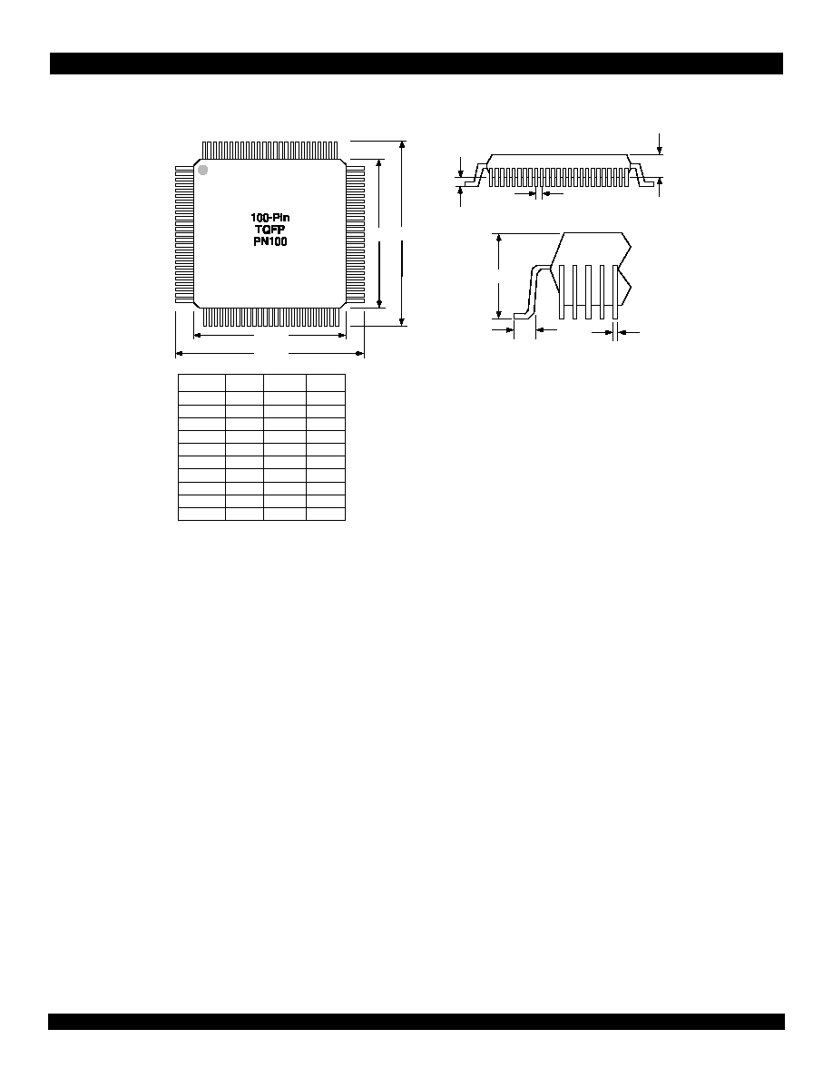
Package Drawing
Package Drawing
Package Drawing
Package Drawing
2.4792 '
1
100
A1
A2
e
b
L
5.5125 '
D
4.4458 '
D1
A
4.3514 ' 5.4035 '
E1
77v107 drw 01
E
A
A1
A2
D
D1
E
E1
L
e
b
-
0.05
1.35
-
-
-
-
0.45
-
0.17
-
0.10
1.40
16.00
14.00
16.00
14.00
-
0.50
0.22
1.60
0.15
1.45
-
-
-
-
0.75
-
0.27
SYMBOL
MIN.
NOM.
MAX.
Dimensions are in millimeters
For the complete package drawing, see PSC4036.pdf in the packaging section of the IDT web site.

24 of 24
July 3, 2001
IDT77V107
CORPORATE HEADQUARTERS
2975 Stender Way
Santa Clara, CA 95054
for SALES:
800-345-7015 or 408-727-6116
fax: 408-330-1748
www.idt.com
for Tech Support:
email: phyhelp@idt.com
phone: 408-
492-8208
The IDT logo is a registered trademark of Integrated Device Technology, Inc.
Ordering Information
Ordering Information
Ordering Information
Ordering Information
Revision History
Revision History
Revision History
Revision History
1/20/2000:
ADVANCE INFORMATION. Initial release.
2/18/2000
PRELIMINARY. Initial release.
1/4/2001
FINAL. DPI interface option removed, package drawing added, power consumption and Utopia timing limits improved. Corrections to Diag-
nostic Control Register. Description added of symbol framing hunt logic. Corrections to resistor values on "Recommended Connection to
Magnetics" on pages 14 and 15.
4/19/01
Added RXREF waveform and pulse width information in Figure 20.
7/03/01
Corrected 0x03 address register name on page 17 to read "LED Driver and HEC Status/Control Registers."
Package
IDT
NNNNN
Device Type
A
Power
NNN
Speed
A
A
Process/
Temp. Range
Blank
25
Speed in Mb/s
77V107
25Mbps ATM Single PHY with
Utopia 2
Commercial (0∞C to +70∞C)
5362 drw 50
L
PF
100-Lead TQFP (PN-100)
I
Industrial (-40∞C to +85∞C)