 | ÐлекÑÑоннÑй компоненÑ: 79R4640 | СкаÑаÑÑ:  PDF PDF  ZIP ZIP |
4640ds.fm
1 of 23
April 10, 2001
2001 Integrated Device Technology, Inc.
DSC 3486/2
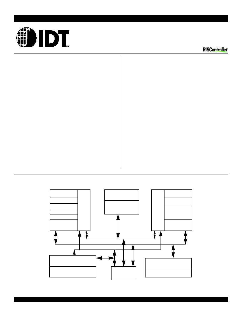
Block Diagram
Block Diagram
Block Diagram
Block Diagram
The IDT logo is a registered trademark and RC4600, RC4650, RC3081,RC3052,RC3051,RC3041 RISController, and RISCore are trademarks of Integrated Device Technology, Inc.
267 MHz 64-bit CPU
64-bit Register File
64-bit Adder
Store Aligner
Logic Unit
Load Aligner
High-Performance
Integer Multiply
P
i
pe
l
i
n
e
C
o
nt
r
o
l
FP Register File
FP Add/Sub/Cvt/
Pack/Unpack
FP Multiply
P
i
pe
li
ne
C
ont
r
o
l
89 MFlops Single-Precision FPA
Div/Sqrt
32-bit
Synchronized
System Interface
Address Translation/
Cache Attribute Control
Exception Management
Functions
System Control Coprocessor
Data Cache
Data Cache
Instruction Bus
Control Bus
Data Bus
Set A
(Lockable)
Set B
Instruction Cache
Set B
Instruction Cache
Set A
(Lockable)
Features
Features
Features
Features
x
High-performance embedded 64-bit microprocessor
64-bit integer operations
64-bit registers
Based on the MIPS RISC Architecture
100MHz, 133MHz, 150MHz, 180MHz, 200MHz and 267MHz
operating frequencies
32-bit bus interface brings 64-bit power to 32-bit system cost
x
High-performance DSP capability
133.5 Million Integer Mul-Accumulate
operations/sec @267MHz
89 MFlops floating-point operations @267MHz
x
High-performance microprocessor
133.5 M Mul-Add/second @267MHz
89 MFlops @267MHz
>640,000 dhrystone (2.1)/sec capability @267MHz (352
dhrystone MIPS)
x
High level of integration
64-bit, 267 MHz integer CPU
8KB instruction cache; 8KB data cache
Integer multiply unit with 133.5M Mul-Add/sec
x
Upwardly software compatible with IDT RISController
Family
x
Easily upgradable to 64-bit system
x
Low-power operation
Active power management powers-down inactive units
Standby mode
x
Large, efficient on-chip caches
Separate 8KB Instruction and 8KB Data caches
Over 3200MB/sec bandwidth from internal caches
2-set associative
Write-back and write-through support
Cache locking, to facilitate deterministic response
High performance write protocols, for graphics and data
communications
x
Bus compatible with RC4000 family
System interfaces to 125MHz, provides bandwidth up to 500
MB/sec
Direct interface to 32-bit wide systems
Synchronized to external reference clock for multi- master
operation
Socket compatible with IDT RC 64474 and RC64574
x
Improved real-time support
Fast interrupt decode
Optional cache locking
Note: "R" refers to 5V parts; "RV" refers to 3.3V parts; "RC"
refers to both
Low-Cost Embedded
64-bit RISController
w/ DSP Capability
IDT79RC4640
TM
2 of 23
April 10, 2001
IDT79RC4640TM
Description
Description
Description
Description
The IDT79RC4640 is a low-cost member of the Integrated Device
Technology, Inc. RC4000 family, targeted to a variety of performance-
hungry embedded applications. The RC4640 continues the RC4000
tradition of high-performance through high-speed pipelines, high-band-
width caches and bus interface, 64-bit architecture, and careful attention
to efficient control. The cost of this performance is reduced by removing
functional units frequently not required for many embedded applications.
The RC4640 supports a wide variety of embedded processor-based
applications, such as internetworking equipment (routers, switches),
office automation equipment (printers, scanners), and consumer multi-
media game systems. Also, being upwardly software-compatible with
the RC32300 family as well as bus- and upwardly software-compatible
with the IDT RC4000 family, the RC4640 will serve in many of the same
applications. And, the RC4640 supports applications that require integer
digital signal processing (DSP) functions.
The RC64475 and RC64575 processors offer a direct migration path
for designs based on IDT's RC4650 processors, through full pin and
socket compatibility.
The RC4640 brings 64-bit performance levels to lower cost systems.
High performance is preserved by retaining large on-chip two-way set-
associative caches, a streamlined high-speed pipeline, high bandwidth,
64-bit execution, and facilities such as early restart for data cache
misses.
These techniques allow the system designer over 3.2 GB/sec aggre-
gate internal bandwidth, 500 MB/sec bus bandwidth, almost 352 Dhrys-
tone MIPS, 89MFlops, and 133.5 M Mul-Add/sec. An array of tools
facilitates rapid development of RC4640-based systems, allowing a
wide variety of customers access to the processor's high-performance
capabilities while maintaining short time-to-market goals.
Hardware Overview
Hardware Overview
Hardware Overview
Hardware Overview
Some key elements of the RC4640 are briefly described below. More
detailed information is available in the IDT79RC4640/IDT79RC4650
RISC Processor Hardware User's Manual.
Pipeline
Pipeline
Pipeline
Pipeline
The RC4640 uses a 5-stage pipeline that is similar to the
IDT79RC3000 and the IDT79RC4700 processors. The simplicity of this
pipeline allows the RC4640 to cost less than super-scalar processors
and require less power than super-pipelined processors. So, unlike
superscalar processors, applications that have large data dependen-
cies, or require frequent load/stores, can still achieve peak performance.
Integer Execution Engine
Integer Execution Engine
Integer Execution Engine
Integer Execution Engine
The RC4640 implements the MIPS-III Instruction Set Architecture
and is fully upward compatible with applications that run on earlier
generation parts. The RC4640 is software-compatible with the RC4650,
and includes the instruction set found in the RC4700 microprocessor,
targeted at higher performance while maintaining binary compatibility
with RC32300 processors.
The extensions result in better code density, greater multi-
processing support, improved performance for commonly used code
sequences in operating system kernels, and faster execution of floating-
point intensive applications. All resource dependencies are made trans-
parent to the programmer, insuring transportability among implementa-
tions of the MIPS instruction set architecture. In addition, MIPS-III
specifies new instructions defined to take advantage of the 64-bit archi-
tecture of the processor.
Finally, the RC4640 also implements additional instructions, which
are considered extensions to the MIPS-III architecture. These instruc-
tions improve the multiply and multiply-add throughput of the CPU,
making it well suited to a wide variety of imaging and DSP applications.
These extensions, which use opcodes allocated by MIPS Technologies
for this purpose, are supported by a wide variety of development tools.
The MIPS integer unit implements a load/store architecture with
single cycle ALU operations (logical, shift, add, sub) and autonomous
multiply/divide unit. The 64-bit register resources include: 32 general-
purpose orthogonal integer registers, the HI/LO result registers for the
integer multiply/divide unit, and the program counter. In addition, the on-
chip floating-point co-processor adds 32 floating-point registers, and a
floating-point control/status register.
Register File
Register File
Register File
Register File
The RC4640 has 32 general-purpose 64-bit registers. These regis-
ters are used for scalar integer operations and address calculation. The
register file consists of two read ports and one write port and is fully
bypassed to minimize operation latency in the pipeline.
Arithmetic Logic Unit
Arithmetic Logic Unit
Arithmetic Logic Unit
Arithmetic Logic Unit
The RC4640 ALU consists of the integer adder and logic unit. The
adder performs address calculations in addition to arithmetic operations;
the logic unit performs all of the logic and shift operations. Each unit is
highly optimized and can perform an operation in a single pipeline cycle.
Integer Multiply/Divide
Integer Multiply/Divide
Integer Multiply/Divide
Integer Multiply/Divide
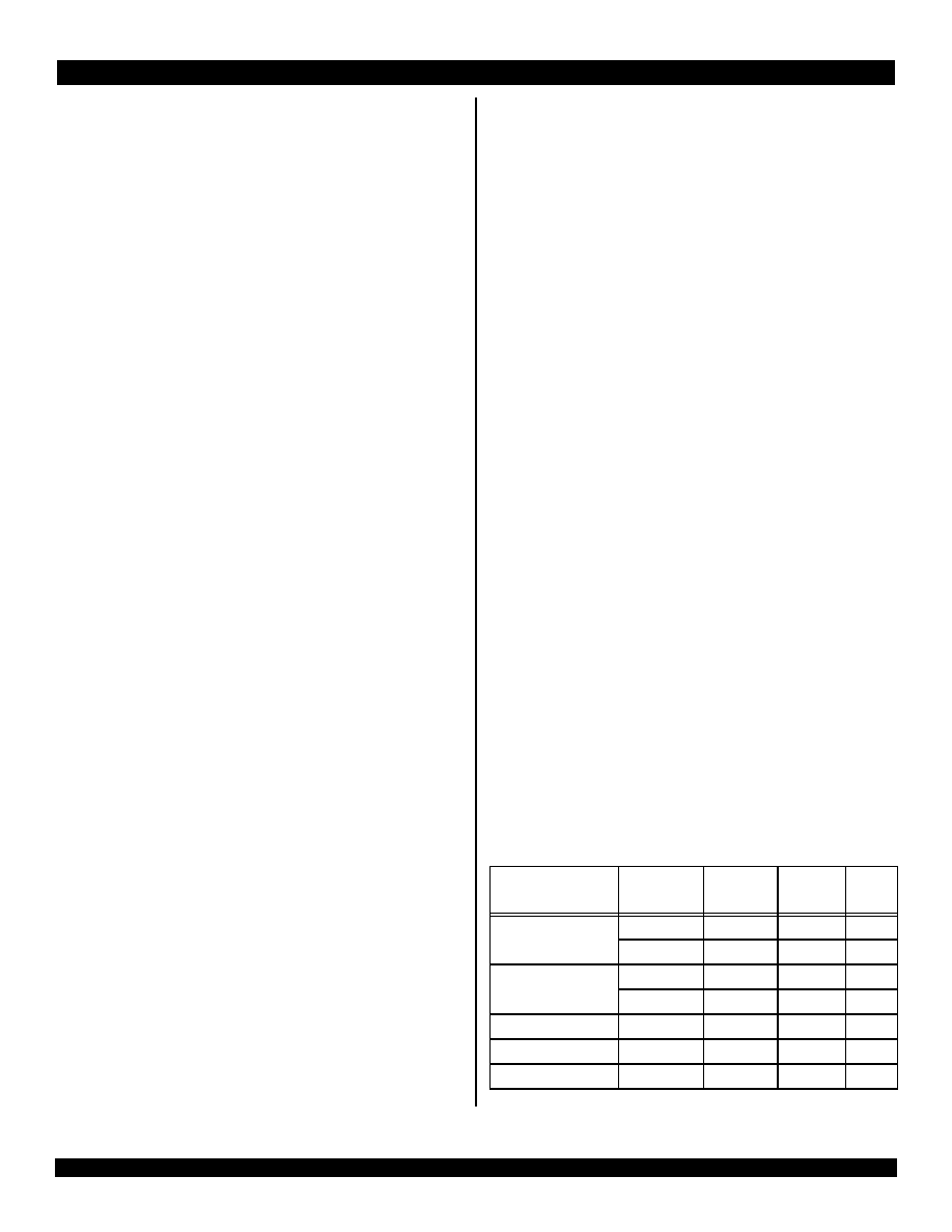
The RC4640 uses a dedicated integer multiply/divide unit, optimized
for high-speed multiply and multiply-accumulate operation. Table 1
shows the performance, expressed in terms of pipeline clocks, achieved
by the RC4640 integer multiply unit.
Opcode
Operand
Size
Latency Repeat Stall
MULT/U, MAD/U
16 bit
3
2
0
32 bit
4
3
0
MUL
16 bit
3
2
1
32 bit
4
3
2
DMULT, DMULTU
any
6
5
0
DIV, DIVU
any
36
36
0
DDIV, DDIVU
any
68
68
0
Table 1 RC4640 Integer Multiply Operation
3 of 23
April 10, 2001
IDT79RC4640TM
The MIPS-III architecture defines that the results of a multiply or
divide operation are placed in the HI and LO registers. The values can
then be transferred to the general purpose register file using the MFHI/
MFLO instructions.
The RC4640 adds a new multiply instruction, "MUL", which can
specify that the multiply results bypass the "Lo" register and are placed
immediately in the primary register file. By avoiding the explicit "Move-
from-Lo" instruction required when using "Lo", throughput of multiply-
intensive operations is increased.
An additional enhancement offered by the RC4640 is an atomic
"multiply-add" operation, MAD, used to perform multiply-accumulate
operations. This instruction multiplies two numbers and adds the product
to the current contents of the HI and LO registers. This operation is used
in numerous DSP algorithms, and allows the RC4640 to cost reduce
systems requiring a mix of DSP and control functions.
Finally, aggressive implementation techniques feature low latency for
these operations along with pipelining to allow new operations to be
issued before a previous one has fully completed. Table 1 also shows
the repeat rate (peak issue rate), latency, and number of processor stalls
required for the various operations. The RC4640 performs automatic
operand size detection to determine the size of the operand, and imple-
ments hardware interlocks to prevent overrun, allowing this high-perfor-
mance to be achieved with simple programming.
Floating-Point Coprocessor
Floating-Point Coprocessor
Floating-Point Coprocessor
Floating-Point Coprocessor
The RC4640 incorporates an entire single-precision floating-point
coprocessor on chip, including a floating-point register file and execution
units. The floating-point coprocessor forms a "seamless" interface with
the integer unit, decoding and executing instructions in parallel with the
integer unit.
The floating-point unit of the RC4640 directly implements single-
precision floating-point operations, which enables the RC4640 to
perform functions such as graphics rendering without requiring exten-
sive die area or power consumption. The single-precision unit of the
RC4640 is directly compatible with the single-precision operation of the
RC4700, and features the same latencies and repeat rates.
The RC4640 does not directly implement the double-precision opera-
tions found in the RC4700. However, to maintain software compatibility,
the RC4640 will signal a trap when a double-precision operation is initi-
ated, allowing the requested function to be emulated in software. Alter-
natively, the system architect could use a software library emulation of
double-precision functions, selected at compile time, to eliminate the
overhead associated with trap and emulation.
Floating-Point Units
Floating-Point Units
Floating-Point Units
Floating-Point Units
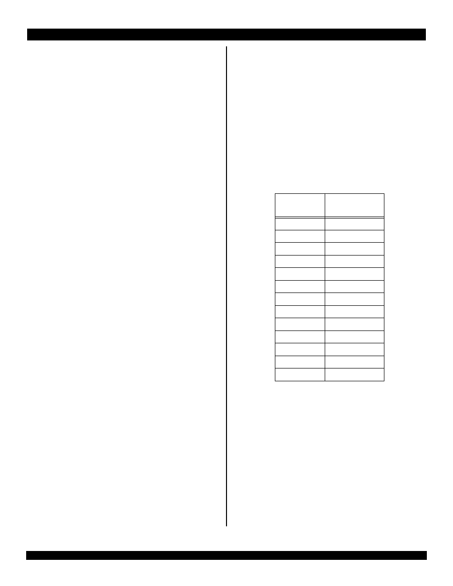
The RC4640's floating-point execution units perform single precision
arithmetic, as specified in IEEE Standard 754. The execution unit is
broken into a separate multiply unit and a combined add/convert/divide/
square root unit. Overlap of multiply and add/subtract is supported. The
multiplier is partially pipelined, allowing a new multiplication instruction
to begin every 6 cycles.
As in the IDT79RC4700, the RC4640 maintains fully precise floating-
point exceptions while allowing both overlapped and pipelined opera-
tions. Precise exceptions are extremely important in mission-critical
environments, such as ADA, and highly desirable for debugging in any
environment.
The floating-point unit's operation set includes floating-point add,
subtract, multiply, divide, square root, conversion between fixed-point
and floating-point format, conversion among floating-point formats, and
floating-point compare. These operations comply with IEEE Standard
754. Double precision operations are not directly supported; attempts to
execute double-precision floating point operations, or refer directly to
double-precision registers, result in the RC4640 signalling a "trap" to the
CPU, enabling emulation of the requested function. Table 2 gives the
latencies of some of the floating-point instructions in internal processor
cycles.
Floating-Point General Register File
Floating-Point General Register File
Floating-Point General Register File
Floating-Point General Register File
The floating-point register file is made up of thirty-two 32-bit regis-
ters. These registers are used as source or target registers for the
single-precision operations.
References to these registers as 64-bit registers (as supported in the
RC4700) will cause a trap to be signalled to the integer unit.
The floating-point control register space contains two registers; one
for determining configuration and revision information for the copro-
cessor and one for control and status information. These are primarily
involved with diagnostic software, exception handling, state saving and
restoring, and control of rounding modes.
Operation
Instruction
Latency
ADD
4
SUB
4
MUL
8
DIV
32
SQRT
31
CMP
3
FIX
4
FLOAT
6
ABS
1
MOV
1
NEG
1
LWC1
2
SWC1
1
Table 2 Floating-Point Operation
4 of 23
April 10, 2001
IDT79RC4640TM
System Control Coprocessor (CP0)
System Control Coprocessor (CP0)
System Control Coprocessor (CP0)
System Control Coprocessor (CP0)
The system control coprocessor in the MIPS architecture is respon-
sible for the virtual to physical address translation and cache protocols,
the exception control system, and the diagnostics capability of the
processor. In the MIPS architecture, the system control coprocessor
(and thus the kernel software) is implementation dependent.
In the RC4640, significant changes in CP0 relative to the RC4600
have been implemented. These changes are designed to simplify
memory management, facilitate debug, and speed real-time processing.
System Control Coprocessor Registers
System Control Coprocessor Registers
System Control Coprocessor Registers
System Control Coprocessor Registers
The RC4640 incorporates all system control co-processor (CP0)
registers on-chip. These registers provide the path through which the
virtual memory system's address translation is controlled, exceptions
are handled, and operating modes are controlled (kernel vs. user mode,
interrupts enabled or disabled, cache features). In addition, the RC4640
includes registers to implement a real-time cycle counting facility, which
aids in cache diagnostic testing, assists in data error detection, and facil-
itates software debug. Alternatively, this timer can be used as the
operating system reference timer, and can signal a periodic interrupt.
Table 3 shows the CP0 registers of the RC4640.
Number
Name
Function
0
IBase
Instruction address space base
1
IBound
Instruction address space bound
2
DBase
Data address space base
3
DBound
Data address space bound
4-7, 10, 20-25,
29, 31
-
Not used
8
BadVAddr
Virtual address on address exceptions
9
Count
Counts every other cycle
11
Compare
Generate interrupt when Count = Compare
12
Status
Miscellaneous control/status
13
Cause
Exception/Interrupt information
14
EPC
Exception PC
15
PRId
Processor ID
16
Config
Cache and system attributes
17
CAlg
Cache attributes for the 8 512MB regions of the
virtual address space
18
IWatch
Instruction breakpoint virtual address
19
DWatch
Data breakpoint virtual address
26
ECC
Used in cache diagnostics
27
CacheErr
Cache diagnostic information
28
TagLo
Cache index information
30
ErrorEPC
CacheError exception PC
Table 3 RC4640 CPO Registers
Operation Modes
Operation Modes
Operation Modes
Operation Modes
The RC4640 supports two modes of operation: user mode and
kernel mode. Kernel mode operation is typically used for exception
handling and operating system kernel functions, including CP0 manage-
ment and access to IO devices. In kernel mode, software has access to
the entire address space and all of the co-processor 0 registers, and
can select whether to enable co-processor 1 accesses. The processor
enters kernel mode at reset, and whenever an exception is recognized.
User mode is typically used for applications programs. User mode
accesses are limited to a subset of the virtual address space, and can
be inhibited from accessing CP0 functions.
Virtual-to-Physical Address Mapping
Virtual-to-Physical Address Mapping
Virtual-to-Physical Address Mapping
Virtual-to-Physical Address Mapping
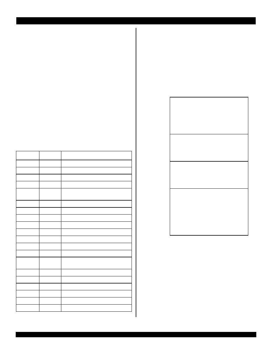
The 4GB virtual address space of the RC4640 is shown in Figure 1.
The 4 GB address space is divided into addresses accessible in either
kernel or user mode (kuseg), and addresses only accessible in kernel
mode (kseg2:0).
The RC4640 supports the use of multiple user tasks sharing
common virtual addresses, but mapped to separate physical addresses.
This facility is implemented via the "base-bounds" registers contained in
CP0.
When a user virtual address is asserted (load, store, or instruction
fetch), the RC4640 compares the virtual address with the contents of
the appropriate "bounds" register (instruction or data). If the virtual
0xFFFFFFFF
0xC0000000
Kernel virtual address space
(kseg2)
Unmapped, 1.0 GB
0xBFFFFFFF
0xA0000000
Uncached kernel physical address space
(kseg1)
Unmapped, 0.5GB
0x9FFFFFFF
0x80000000
Cached kernel physical address space
(kseg0)
Unmapped, 0.5GB
0x7FFFFFF
0x00000000
User virtual address space
(useg)
Mapped, 2.0GB
Figure 1 Mode Virtual Addressing (32-bit mode)
5 of 23
April 10, 2001
IDT79RC4640TM
address is "in bounds", the value of the corresponding "base" register is
added to the virtual address to form the physical address for that refer-
ence. If the address is not within bounds, an exception is signalled.
This facility enables multiple user processes in a single physical
memory without the use of a TLB. This type of operation is further
supported by a number of development tools for the RC4640, including
real-time operating systems and "position independent code".
Kernel mode addresses do not use the base-bounds registers, but
rather undergo a fixed virtual-to-physical address translation.
Debug Support
Debug Support
Debug Support
Debug Support
To facilitate software debug, the RC4640 adds a pair of "watch" regis-
ters to CP0. When enabled, these registers will cause the CPU to take
an exception when a "watched" address is appropriately accessed.
Interrupt Vector
Interrupt Vector
Interrupt Vector
Interrupt Vector
The RC4640 also adds the capability to speed interrupt exception
decoding. Unlike the RC4700, which utilizes a single common exception
vector for all exception types (including interrupts), the RC4640 allows
kernel software to enable a separate interrupt exception vector. When
enabled, this vector location speeds interrupt processing by allowing
software to avoid decoding interrupts from general purpose exceptions.
Cache Memory
Cache Memory
Cache Memory
Cache Memory
To keep the RC4640's high-performance pipeline full and operating
efficiently, the RC4640 incorporates on-chip instruction and data caches
that can each be accessed in a single processor cycle. Each cache has
its own 64-bit data path and can be accessed in parallel. The cache
subsystem provides the integer and floating-point units with an aggre-
gate bandwidth of over 3200 MB per second at a pipeline clock
frequency of 267MHz. The cache subsystem is similar in construction to
that found in the RC4700, although some changes have been imple-
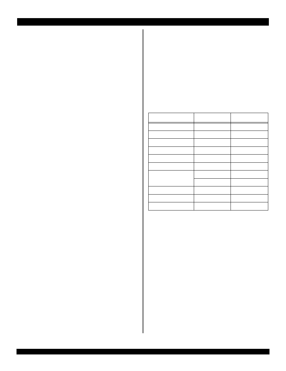
mented. Table 4 is an overview of the caches found on the RC4640.
Instruction Cache
Instruction Cache
Instruction Cache
Instruction Cache
The RC4640 incorporates a two-way set associative on-chip instruc-
tion cache. This virtually indexed, physically tagged cache is 8KB in size
and is parity protected.
Because the cache is virtually indexed, the virtual-to-physical
address translation occurs in parallel with the cache access, thus further
increasing performance by allowing these two operations to occur simul-
taneously. The tag holds a 20-bit physical address and valid bit, and is
parity protected.
The instruction cache is 64-bits wide, and can be refilled or accessed
in a single processor cycle. Instruction fetches require only 32 bits per
cycle, for a peak instruction bandwidth of 1068MB/sec at 267MHz.
Sequential accesses take advantage of the 64-bit fetch to reduce power
dissipation, and cache miss refill, can write 64 bits-per-cycle to minimize
the cache miss penalty. The line size is eight instructions (32 bytes) to
maximize performance.
In addition, the contents of one set of the instruction cache (set "A")
can be "locked" by setting a bit in a CP0 register. Locking the set
prevents its contents from being overwritten by a subsequent cache
miss; refill occurs then only into "set B".
This operation effectively "locks" time critical code into one 4kB set,
while allowing the other set to service other instruction streams in a
normal fashion. Thus, the benefits of cached performance are achieved,
while deterministic real-time response is preserved.
Data Cache
Data Cache
Data Cache
Data Cache
For fast, single cycle data access, the RC4640 includes an 8KB on-
chip data cache that is two-way set associative with a fixed 32-byte
(eight words) line size. Table 4 lists the RC4640 cache attributes.
The data cache is protected with byte parity and its tag is protected
with a single parity bit. It is virtually indexed and physically tagged to
allow simultaneous address translation and data cache access
The normal write policy is writeback, which means that a store to a
cache line does not immediately cause memory to be updated. This
increases system performance by reducing bus traffic and eliminating
the bottleneck of waiting for each store operation to finish before issuing
a subsequent memory operation. Software can however select write-
through for certain address ranges, using the CAlg register in CP0.
Cache protocols supported for the data cache are:
x
Uncached.
Addresses in a memory area indicated as uncached will not be
read from the cache. Stores to such addresses will be written
directly to main memory, without changing cache contents.
x
Writeback.
Loads and instruction fetches will first search the cache, reading
main memory only if the desired data is not cache resident. On
data store operations, the cache is first searched to see if the
target address is cache resident. If it is resident, the cache con-
Characteristics
Instruction
Data
Size
8KB
8KB
Organization
2-way set associative 2-way set associative
Line size
32B
32B
Index
vAddr
11..0
vAddr
11..0
Tag
pAddr
31..12
pAddr
31..12
Write policy
n.a.
writeback /writethru
Line transfer order
read sub-block order
read sub-block order
write sequential
write sequential
Miss restart after transfer of entire line
first word
Parity
per-word
per-byte
Cache locking
set A
set A
Table 4 RC4640 Cache Attributes
Document Outline