32365_ds.fm
1 of 44
February 25, 2004
2003 Integrated Device Technology, Inc.
DSC 6210
IDT and the IDT logo are registered trademarks of Integrated Device Technology, Inc.
Device Overview
Device Overview
Device Overview
Device Overview
The RC32365 device is a member of the IDTTM InterpriseTM family of
integrated communications processors. This device is designed to
address a range of communications applications that require the effi-
cient processing of IPSec algorithms. These applications include gate-
ways, wireless access points, and virtual private network (VPN)
equipment. The key to the RC32365's efficient processing of IPSec
algorithms is a highly progammable security engine which off-loads the
CPU core of encryption/decryption, hashing, and padding tasks.
F
F
F
Features List
eatures List
eatures List
eatures List
x
RC32300 32-bit CPU core
32-bit MIPS instruction set
Supports big or little endian operation
MMU
16-entry TLB
Supports variable page sizes and enhanced write algo-
rithm
Supports variable number of locked entries
8KB Instruction Cache
2-way set associative
LRU replacement algorithm
4 word line size
Sub-block ordering
Word parity
Per line cache locking
2KB Data Cache
2-way set associative
LRU replacement algorithm
4 word line size
Sub-block ordering
Byte parity
Per line cache locking
Can be programmed on a page basis to implement write-
through no write allocate, write-through write allocate, or
write-back algorithms
Enhanced EJTAG and JTAG Interfaces
Compatible with IEEE Std. 1149.1-1990
x
Security Engine
Dedicated DMA channels for high speed data transfers to and
from the security engine
On-chip memory for storage of two security contexts
Supports ECB and CBC modes for the following symmetric
encryption algorithms: DES, triple DES (both two key (k1=k3)
and three key (k1!=k3) modes), AES-128 with 128-bit blocks,
AES-192 with 128-bit blocks
Hardware support for encryption pad generation and checking
using one of seven popular padding algorithms: supports pad
algorithm required by IPSec ESP
Supports MD5 and SHA-1 one-way hash functions
Programmable truncation length of computed hash and HMAC
on a security context basis
Supports concurrent hash and encryption operations
B
B
B
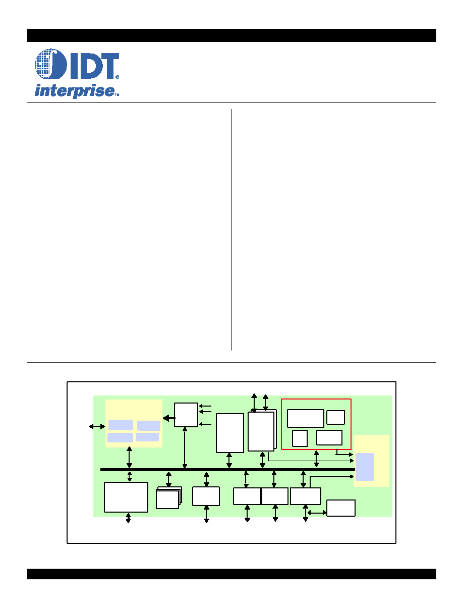
Block Diagram
lock Diagram
lock Diagram
lock Diagram
Figure 1 RC32365 Internal Block Diagram
EJTAG
MMU
D. Cache
I. Cache
32-bit MIPS
CPU Core
JTAG
Interrupt
Controller
3 Counter
Timers
Bus/System
DMA
Controller
Arbiter
SDRAM & Device
UART
(16550)
GPIO
Interface
PCI
Master/Target
Memory &
Peripheral Bus
Serial Channel
GPIO Pins
PCI Bus
Controller
SPI
SPI Bus
MII
MII
Integrity
Monitor
IPBus
TM
Interface
PCI Arbiter
(Host Mode)
.
.
Security Functions
Security
Context Storage
RNG
Encryption
Unit
Unit
Hash
10/100
2 Ethernet
Interfaces
Controllers
including PCMCIA
Support
(including PCMCIA)
RC32365
IDT
TM
Interprise
TM
Integrated
Communications Processor

2 of 44
February 25, 2004
RC32365
Optimized for IPSec AH, ESP, and AH+ESP (single MAC)
tunnel and transport mode processing: initialization Vector (IV)
insertion and extraction, HMAC checking, AH mutable field
processing for both IPv4 and IPv6 packets, IPSec pad gener-
ation and checking
x
Random Number Generator
True hardware random number generator suitable for security
applications: may be used to generate symmetric and public
keys, initialization vectors, and nonces
Dedicated DMA engine for transferring random numbers to
memory
Generates random numbers at a bit rate equal to IPBus clock
frequency divided by 32
Provides 4 word (16 byte) FIFO to queue random numbers
Randomness tester continually verifies proper operation of
random number generator using a randomness test defined in
FIPS 140-2
x
PCI Interface
32-bit PCI revision 2.2 compliant
Supports host or satellite operation in both master and target
modes
PCI clock: supports frequencies from 16 MHz to 66 MHz, PCI
clock may be asynchronous to master clock (CLK)
PCI arbiter in Host mode: supports 3 external masters, fixed
priority or round robin arbitration
I
2
O "like" PCI Messaging Unit
x
Two Ethernet Interfaces
10 and 100 Mb/s ISO/IEC 8802-3:1996 compliant
Two IEEE 802.3u compatible Media Independent Interfaces
(MII) with serial management interface
MII supports IEEE 802.3u auto-negotiation speed selection
Supports 64 entry hash table based multicast address filtering
512 byte transmit and receive FIFOs
Supports flow control functions outlined in IEEE Std. 802.3x-
1997
x
SDRAM Controller
Supports up to 512 MB of memory
2 chip selects (each supports 2 or 4 banks internal SDRAM
banks)
32-bit data width, supports 8/16/32-bit width devices
Supports 16Mb, 64Mb, 128Mb, and 256Mb, and 512Mb
devices
Automatic refresh generation
x
Memory and Peripheral Device Controller
Provides "glueless" interface to standard SRAM, Flash, ROM,
dual-port memory, and peripheral devices
Provides "glueless" interface to many 16-bit PCMCIA devices
Demultiplexed address and data buses: 32-bit data bus, 26-bit
address bus, 6 chip selects, control for external data bus
buffers
Supports 8-bit, 16-bit, and 32-bit width devices: automatic byte
gathering and scattering
Flexible protocol configuration parameters: programmable
number of wait states (0 to 63), programmable postread/post-
write delay (0 to 31), supports external wait state generation,
supports Intel and Motorola style peripherals
Write protect capability per chip select
Programmable bus transaction timer generates warm reset
when counter expires
Supports up to 64MB of memory per chip select
x
DMA Controller
9 DMA channels: two channels for each of the two Ethernet
interfaces (transmit/receive), two channels for PCI (PCI to
Memory and Memory to PCI), two channels for security engine
(input/output), one channel for the hardware random number
generator
Provides flexible descriptor based operation
Supports unaligned transfers (i.e., source or destination
address may be on any byte boundary) with arbitrary byte
length
x
General Purpose Peripherals
Serial port compatible with 16550 Universal Asynchronous
Receiver Transmitter (UART)
Three general purpose 32-bit counter/timers
Interrupt Controller
Serial Peripheral Interface (SPI) supporting host mode
16 general purpose I/O (GPIO) pins which can be configured
as interrupt sources
x
System Features
JTAG Interface (IEEE Std. 1149.1 compatible)
256 pin CABGA package
2.5V core supply and 3.3V I/O supply
C
C
C
CPU Execution Core
PU Execution Core
PU Execution Core
PU Execution Core
The RC32365 is built around the RC32300 32-bit high performance
microprocessor core. The RC32300 implements the enhanced MIPS-II
ISA and helps meet the real-time goals and maximize throughput of
communications and consumer systems by providing capabilities such
as a prefetch instruction, multiple DSP instructions, and cache locking.
The instruction set is largely compatible with the MIPS32 instruction set,
allowing the customer to select from a broad range of software and
development tools. Cache locking guarantees real-time performance by
holding critical code and parameters in the cache for immediate avail-
ability. The microprocessor also i mplements an on-chip MMU with a
TLB, making the it fully compliant with the requirements of real time
operating systems.
Security Engine
Security Engine
Security Engine
Security Engine
The RC32365 incorporates an on-chip security engine that has been
designed to accelerate IPSec performance and minimize the amount of
performance required by the CPU to process secure packet traffic. The
engine includes hardware support for the DES, 3DES, and AES encryp-
tion algorithms and the MD5 and SHA1 hash functions. The engine also
supports hardware-assisted packet processing for the various modes of
IPSec, including AH, ESP, and AH+ESP tunnel and transport modes.
Two dedicated DMA channels are used to transfer data to and from the
security engine, allowing the CPU to work on other tasks during this
time.

3 of 44
February 25, 2004
RC32365
PCI Interface
PCI Interface
PCI Interface
PCI Interface
The PCI interface on the RC32365 is compatible with version 2.2 of
the PCI specification. An on-chip arbiter supports up to three external
bus masters, supporting both fixed priority and rotating priority arbitra-
tion schemes. The RC32365 can support both satellite and host PCI
configurations, enabling it to act as a slave controller for a PCI add-in
card application, or as the primary PCI controller in the system. The PCI
interface can be operated synchronously or asynchronously to the other
I/O interfaces on the RC32365 device.
PCMCIA Interface
PCMCIA Interface
PCMCIA Interface
PCMCIA Interface
The RC32365 provides a "glueless" connection to a single PCMCIA
I/O device via the memory and peripheral device controller. The
PCMCIA interface allows the RC32365 to connect to various types of I/O
peripherals including fax modems, storage devices, and wireless LAN
chipsets. The RC32365 implementation provides a maximum
throughput of 160 Mbps through the 16-bit wide interface as specified by
the PCMCIA 2.1 Standard.
Ethernet Interface
Ethernet Interface
Ethernet Interface
Ethernet Interface
The RC32365 has two Ethernet Channels supporting 10Mbps and
100Mbps speeds and provides a standard media independent interface
(MII) off-chip, allowing a wide range of external devices to be connected
efficiently.
M
M
M
Memory and I
emory and I
emory and I
emory and I////O Controller
O Controller
O Controller
O Controller
The RC32365 incorporates a flexible memory and peripheral device
controller providing direct support for SDRAM, Flash ROM, SRAM,
PCMCIA, and other I/O devices. It can interface directly to 8-bit boot
ROM for a very low cost system implementation. It also offers various
trade-offs in cost / performance for the main memory architecture. The
timers implemented on the RC32365 satisfy the requirements of most
real time operating systems.
DMA Controller
DMA Controller
DMA Controller
DMA Controller
The DMA controller off-loads the CPU core from moving data among
the on-chip interfaces, external peripherals, and memory. The DMA
controller supports scatter / gather DMA with no alignment restrictions,
appropriate for communications and graphics systems.
E
E
E
Enhanced JTAG Interface
nhanced JTAG Interface
nhanced JTAG Interface
nhanced JTAG Interface
For system debugging, the RC32300 CPU core includes an
Enhanced JTAG (EJTAG) interface which operates in Run-Time Mode.
T
T
T
Thermal Considerations
hermal Considerations
hermal Considerations
hermal Considerations
The RC32365 is guaranteed in a ambient temperature range of 0
°
to
+70
°
C for commercial temperature devices and - 40
°
to +85
°
for indus-
trial temperature devices.
R
R
R
Revision Histor
evision Histor
evision Histor
evision Historyyyy
March 17, 2003: Initial publication.
May 15, 2003: Removed "write protect capability" from features of
the SDRAM Controller.
July 9, 2003: In Table 6, changed values for RSTN (output).
Changed values in Tables 7, 8, 9, 10, and 17.
October 3, 2003: Added 180 MHz speed grade. Changed min
values in Table 7 from 1.8 to 1.2 for all signals except SDCLKINP and
SDCKENP. Changed min values for Tdo 10b and 10c in Table 10 for
PCIBEN, etc. and PCIGNTN/PCIREQN from 2.0 to 1.5.
February 25, 2004: Deleted reference to RNGCLK in Table 1
(GPIO[6]) and Table 22.

4 of 44
February 25, 2004
RC32365
P
P
P
Pin Description Table
in Description Table
in Description Table
in Description Table
The following table lists the functions of the pins provided on the RC32365. Some of the functions listed may be multiplexed onto the same pin
(indicated as alternate functions).
To define the active polarity of a signal, a suffix will be used. Signals ending with an "N" should be interpreted as being active, or asserted, when at
a logic zero (low) level. All other signals (including clocks, buses, and select lines) will be interpreted as being active, or asserted, when at a logic one
(high) level.
Signal
Type
Name/Description
Memory and Peripheral Bus
BDIRN
O
External Buffer Direction. Memory and peripheral bus external data bus buffer direction control.
If the RC32365 memory and peripheral bus is connected to the A side of a transceiver such as an
IDT74FCT245, then this pin may be directly connected to the direction control (e.g., BDIR) pin of
the transceiver.
BOEN[1:0]
O
External Buffer Enable. These signals provide output enable control for external buffers on the
memory and peripheral data bus.
BWEN[3:0]
O
Byte Write Enables. These signals are memory and peripheral bus byte write enable signals.
BWEN[0] corresponds to byte lane MDATA[7:0]
BWEN[1] corresponds to byte lane MDATA[15:8]
BWEN[2] corresponds to byte lane MDATA[23:16]
BWEN[3] corresponds to byte lane MDATA[31:24]
CSN[5:0]
O
Chip Selects. These signals are used to select an external device on the memory and peripheral
bus.
MADDR[21:0]
O
Address Bus. 22-bit memory and peripheral bus address bus.
MADDR[25:22] are available as GPIO[5:2] alternate functions.
MDATA[31:0]
I/O
Data Bus. 32-bit memory and peripheral data bus. During a cold reset, bits 0 through 16 of this
data bus function as inputs that are used to load the boot configuration vector.
OEN
O
Output Enable. This signal is asserted when data should be driven by an external device on the
memory and peripheral bus.
RWN
O
Read Write. This signal indicates whether the transaction on the memory and peripheral bus is a
read transaction or a write transaction. A high level indicates a read from an external device. A
low level indicates a write to an external device.
WAITACKN
I
Wait or Transfer Acknowledge. When configured as wait, this signal is asserted during a mem-
ory and peripheral bus transaction to extend the bus cycle. When configured as a transfer
acknowledge, this signal is asserted during a transaction to signal the completion of the transac-
tion.
RASN
O
SDRAM Row Address Strobe. Row address strobe asserted during memory and peripheral bus
SDRAM transactions.
CASN
O
SDRAM Column Address Strobe. Column address strobe asserted during memory and periph-
eral bus SDRAM transactions.
SDCSN[1:0]
O
SDRAM Chip Selects. These signals are used to select SDRAM device(s) on the memory and
peripheral bus.
SDWEN
O
SDRAM Write Enable. This signal is asserted during memory and peripheral bus SDRAM write
transactions.
SDCLKOUT
O
SDRAM Clock Output. This clock is used for all SDRAM memory and peripheral bus operations.
SDCLKINP
I
SDRAM Clock Input. This clock input is typically a delayed version of SDCLKOUT. Data from the
SDRAMs is sampled using this clock.
Table 1 Pin Description (Part 1 of 6)

5 of 44
February 25, 2004
RC32365
General Purpose I/O
GPIO[0]
I/O
General Purpose I/O. This pin can be configured as a general purpose I/O pin.
Alternate function pin name: U0SOUT
Alternate function: UART channel 0 serial output.
GPIO[1]
I/O
General Purpose I/O. This pin can be configured as a general purpose I/O pin.
Alternate function pin name: U0SINP
Alternate function: UART channel 0 serial input.
GPIO[2]
I/O
General Purpose I/O. This pin can be configured as a general purpose I/O pin.
Alternate function pin name: MADDR[22]
Alternate function: Memory and Peripheral bus address bit 22 (output).
GPIO[3]
I/O
General Purpose I/O. This pin can be configured as a general purpose I/O pin.
Alternate function pin name: MADDR[23]
Alternate function: Memory and Peripheral bus address bit 23 (output).
GPIO[4]
I/O
General Purpose I/O. This pin can be configured as a general purpose I/O pin.
Alternate function pin name: MADDR[24]
Alternate function: Memory and Peripheral bus address bit 24 (output).
GPIO[5]
I/O
General Purpose I/O. This pin can be configured as a general purpose I/O pin.
Alternate function pin name: MADDR[25]
Alternate function: Memory and Peripheral bus address bit 25 (output).
GPIO[6]
I/O
General Purpose I/O. This pin can be configured as a general purpose I/O pin.
The value of this pin may be used as a Counter Timer Clock input.
GPIO[7]
I/O
General Purpose I/O. This pin can be configured as a general purpose I/O pin.
Alternate function pin name: SDCKENP
Alternate function: SDRAM clock enable output
The value of this pin may be used as a Counter Timer Clock input.
GPIO[8]
I/O
General Purpose I/O. This pin can be configured as a general purpose I/O pin.
Alternate function pin name: CEN1
Alternate function: PCMCIA chip enable 1 (CE1#) (output).
GPIO[9]
I/O
General Purpose I/O. This pin can be configured as a general purpose I/O pin.
Alternate function pin name: CEN2
Alternate function: PCMCIA chip enable 2 (CE2#) (output).
GPIO[10]
I/O
General Purpose I/O. This pin can be configured as a general purpose I/O pin.
Alternate function pin name: REGN
Alternate function: PCMCIA Attribute Memory Select (REG#) (output).
GPIO[11]
I/O
General Purpose I/O. This pin can be configured as a general purpose I/O pin.
Alternate function pin name: IORDN
Alternate function: PCMCIA IO Read (IORD#) (output).
GPIO[12]
I/O
General Purpose I/O. This pin can be configured as a general purpose I/O pin.
Alternate function pin name: IOWRN
Alternate function: PCMCIA IO Write (IOWR#) (output).
GPIO[13]
I/O
General Purpose I/O. This pin can be configured as a general purpose I/O pin.
Alternate function pin name: PCIREQN[2]
Alternate function: PCI bus request 2 (output).
GPIO[14]
I/O
General Purpose I/O. This pin can be configured as a general purpose I/O pin.
Alternate function pin name: PCIGNTN[2]
Alternate function: PCI bus grant 2 (output).
Signal
Type
Name/Description
Table 1 Pin Description (Part 2 of 6)
Document Outline