 | ÐлекÑÑоннÑй компоненÑ: 79RC64474 | СкаÑаÑÑ:  PDF PDF  ZIP ZIP |
64474ds.fm
1 of 25
April 10, 2001
2001 Integrated Device Technology, Inc.
DSC 4952
Block diagram
Block diagram
Block diagram
Block diagram
The IDT logo is a registered trademark and RC32134, RC32364, RC64145, RC64474, RC64475, RC4650, RC4640, RC4600,RC4700 RC3081, RC3052, RC3051, RC3041, RISController, and RISCore are trade-
marks of Integrated Device Technology, Inc.
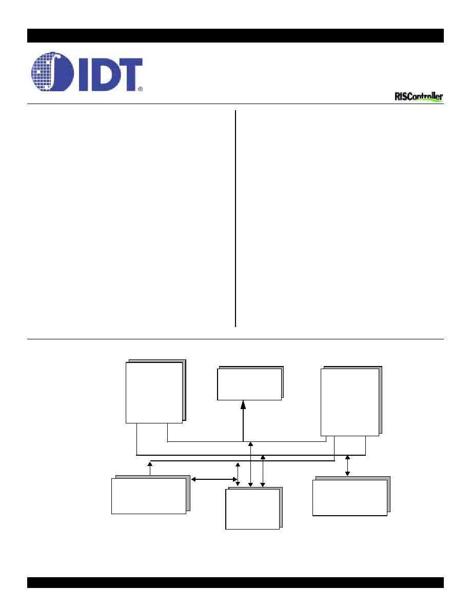
System Control
Coprocessor
(CPO )
Data Cache
(Lockable)
64-bit
330 M IPS
Instruction Cache
(Lockable)
16KB
16KB
RISCore4000
125 M FLO PS
Single/Double
FPA
32-/64-bit
Synchronized
System
Interface
Precision
C o n tro l B u s
In s tru ctio n B u s
D a ta B u s
CPU Core
Features
Features
Features
Features
x
High performance 64-bit microprocessor, based on the
RISCore4000
Minimized branch and load delays, through streamlined
5-stage scalar pipeline.
Single and double precision floating-point unit
125 peak MFLOP/s at 250 MHz
330 Dhrystone MIPS at 250 MHz
Flexible RC4700-compatible MMU
Joint TLB on-chip, for virtual-to-physical address mapping
x
On-chip two-way set associative caches
16KB instruction cache (I-cache)
16KB data cache (D-cache)
x
Optional I-cache and D-cache locking (per set), provides
improved real-time support
x
Enhanced, flexible bus interface allows simple, low-cost
design
64-bit Bus Interface option, 1000MB/s bandwidth support
32-bit Bus Interface option, 500MB/s bandwidth support
SDRAM timing protocol, through delayed data in write cycles
RC4000/RC5000 family bus-protocol compatibility
Bus runs at fraction of pipeline clock (1/2 to 1/8)
x
Implements MIPS-III Instruction Set Architecture (ISA)
x
3.3V core with 3.3V I/O
x
Software compatible with entire RISController Series of
Embedded Microprocessors
x
Industrial temperature range support
x
Active power management
Powers down inactive units, through sleep-mode feature
x
100% pin compatibility between RC64574, RC64474 and
RC4640
x
100% pin compatibility between RC64575, RC64475 and
RC4650
x
RC64474 available in 128-pin QFP package, for 32-bit only
systems
x
RC64475 available in 208-pin QFP package, for full 64/32 bit
systems
x
Simplified board-level testing, through full Joint Test Action
Group (JTAG) boundary scan
x
Windows® CE compliant
RC64474
TM
RC64475
TM
RISController
TM
Embedded
64-bit Microprocessor, based on
RISCore4000
TM
2 of 25
April 10, 2001
RC64474TM RC64475TM
Device Overview
Device Overview
Device Overview
Device Overview
1
1
1
1
Extending Integrated Device Technology's (IDT) RISCore4000 based
choices (see Table 1), the RC64474 and RC64475 are high perfor-
mance 64-bit microprocessors targeted towards applications that require
high bandwidth, real-time response and rapid data processing and are
ideal for products ranging from internetworking equipment (switches,
routers) to multimedia systems such as web browsers, set-top boxes,
video games, and Windows
®
CE based products. These processors are
rated at 330 Dhrystone MIPS and 125 Million floating point operations
per second, at 250 MHz. The internal cache bandwidth for these devices
is over 3GB/second. The 64-bit external bus bandwidth is at more than
1000MB/s, and the 32-bit external bus bandwidth is at 500MB/s.
The RC64474 is packaged in a 128-pin QFP footprint package and
uses a 32-bit external bus, offering the ideal combination of 64-bit
processing power and 32-bit low-cost memory systems. The RC64475
is packaged in a 208-pin QFP footprint package and uses the full 64-bit
external bus. The RC64475 is ideal for applications requiring 64-bit
performance and 64-bit external bandwidth.
IDT's RISCore4000 is a 250MHz 64-bit execution core that uses a
5-stage pipeline, eliminating the "issue restrictions" associated with
other more complex pipelines. The RISCore4000 implements the
MIPS-III Instruction Set Architecture (ISA) and is upwardly compatible
with applications that run on earlier generation parts.
Implementation of the MIPS-III architecture results in 64-bit opera-
tions, improved performance for commonly used code sequences in
1.
Detailed system operation information is provided in the RC64474/RC64475
user's manual.
operating system kernels, and faster execution of floating-point intensive
applications.
The RISCore4000 integer unit implements a load/store architecture
with single cycle ALU operations (logical, shift, add, subtract) and an
autonomous multiply/divide unit. The ALU consists of the integer adder
and logic unit. The adder performs address calculations in addition to
arithmetic operations, and the logic unit performs all of the processor's
logical and shift operations. Each unit is highly optimized and can
perform an operation in a single pipeline cycle. Both 32- and 64-bit data
operations are performed by the RISCore4000, utilizing 32 general
purpose 64-bit registers (GPR) that are used for integer operations and
address calculation. A complete on-chip floating-point co-processor
(CP1), which includes a floating-point register file and execution units,
forms a "seamless" interface, decoding and executing instructions in
parallel with the integer unit.
CP1's floating-point execution units support both single and
double precision arithmetic--as specified in the IEEE Standard 754--
and are separated into a multiply unit and a combined add/convert/
divide/square root unit. Overlap of multiplies and add/subtract is
supported, and the multiplier is partially pipelined, allowing the initiation
of a new multiply instruction every fourth pipeline cycle.
The floating-point register file is made up of thirty-two 64-bit regis-
ters. The floating-point unit can take advantage of the 64-bit wide data
cache and issue a co-processor load or store doubleword instruction in
every cycle. The RISCore4000's system control coprocessor (CP0)
registers are also incorporated on-chip and provide the path through
which the virtual memory system's page mapping is examined and
changed, exceptions are handled, and any operating mode selections
are controlled.
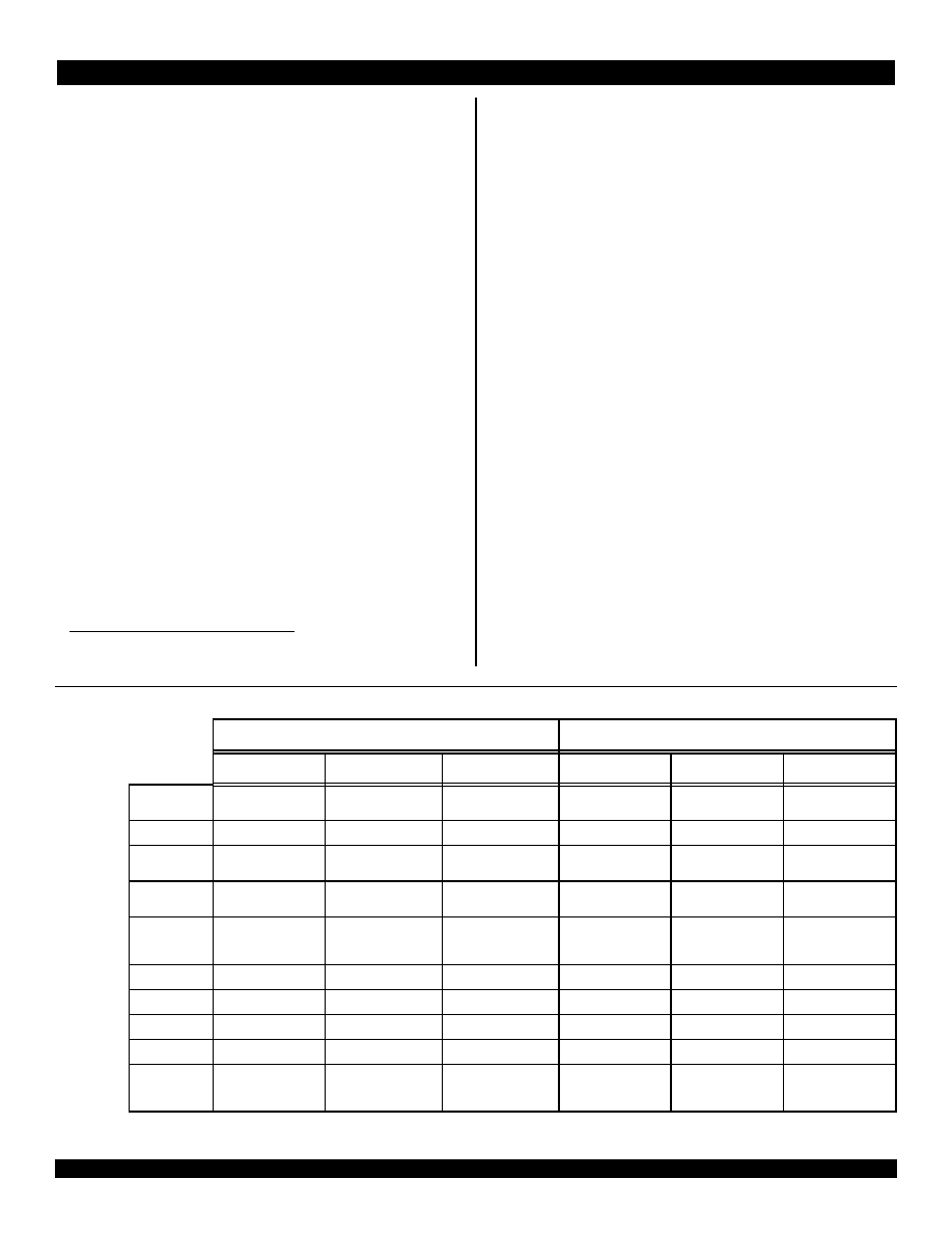
RISCore4000/RISCore5000 Family of Socket Compatible Processors
RISCore4000/RISCore5000 Family of Socket Compatible Processors
RISCore4000/RISCore5000 Family of Socket Compatible Processors
RISCore4000/RISCore5000 Family of Socket Compatible Processors
Table 1 RISCore4000/RISCore5000 Processor Family
32-bit Processors
64-bit Processors
RC4640
RC64474
RC64574
RC4650
RC64475
RC64575
CPU
64-bit RISCore4000
w/ DSP extensions
64-bit RISCore4000
64-bit RISCore5000 w/
DSP extensions
64-bit RISCore4000
w/ DSP extensions
64-bit RISCore4000
64-bit RISCore5000
w/ DSP extensions
Performance
>350MIPS
>330MIPS
>440MIPS
>350MIPS
>330MIPS
>440MIPS
FPA
89 mflops, single pre-
cision only
125 mflops, single and
double precision
666 mflops, single and
double precision
89 mflops, single pre-
cision only
125 mflops, single
and double precision
666 mflops, single
and double precision
Caches
8kB/8kB, 2-way, lock-
able by set
16kB/16kB, 2-way,
lockable by set
32kB/32kB, 2-way,
lockable by line
8kB/8kB, 2-way, lock-
able by set
16kB/16kB, 2-way,
lockable by set
32kB/32kB, 2-way,
lockable by line
External Bus
32-bit
32-bit, Superset pin
compatible w/RC4640
32-bit, Superset pin
compatible w/RC4640,
RC64474
32- or 64-bit
32-or 64-bit, Super-
set pin compatible w/
RC4650
32-or 64-bit, Super-
set pin compatible w/
RC4650, RC64475
Voltage
3.3V
3.3V
2.5V
3.3V
3.3V
2.5V
Frequencies
100-267 MHz
180-250 MHz
200-333 MHz
100-267 MHz
180-250 MHz
200-333 MHz
Packages
128 PQFP
128 QFP
128 QFP
208 QFP
208 QFP
208 QFP
MMU
Base-Bounds
96 page TLB
96 page TLB
Base-Bounds
96 page TLB
96 page TLB
Key Features
Cache locking, on-
chip MAC, 32-bit
external bus
Cache locking, JTAG,
syncDRAM mode, 32-
bit external bus
Cache locking, JTAG,
syncDRAM mode, 32-
bit external bus
Cache locking, on-
chip MAC, 32-bit & 64
bit bus option
Cache locking, JTAG,
syncDRAM mode, 32-
64- bit bus option
Cache locking, JTAG,
syncDRAM mode, 32-
64- bit bus option
3 of 25
April 10, 2001
RC64474TM RC64475TM
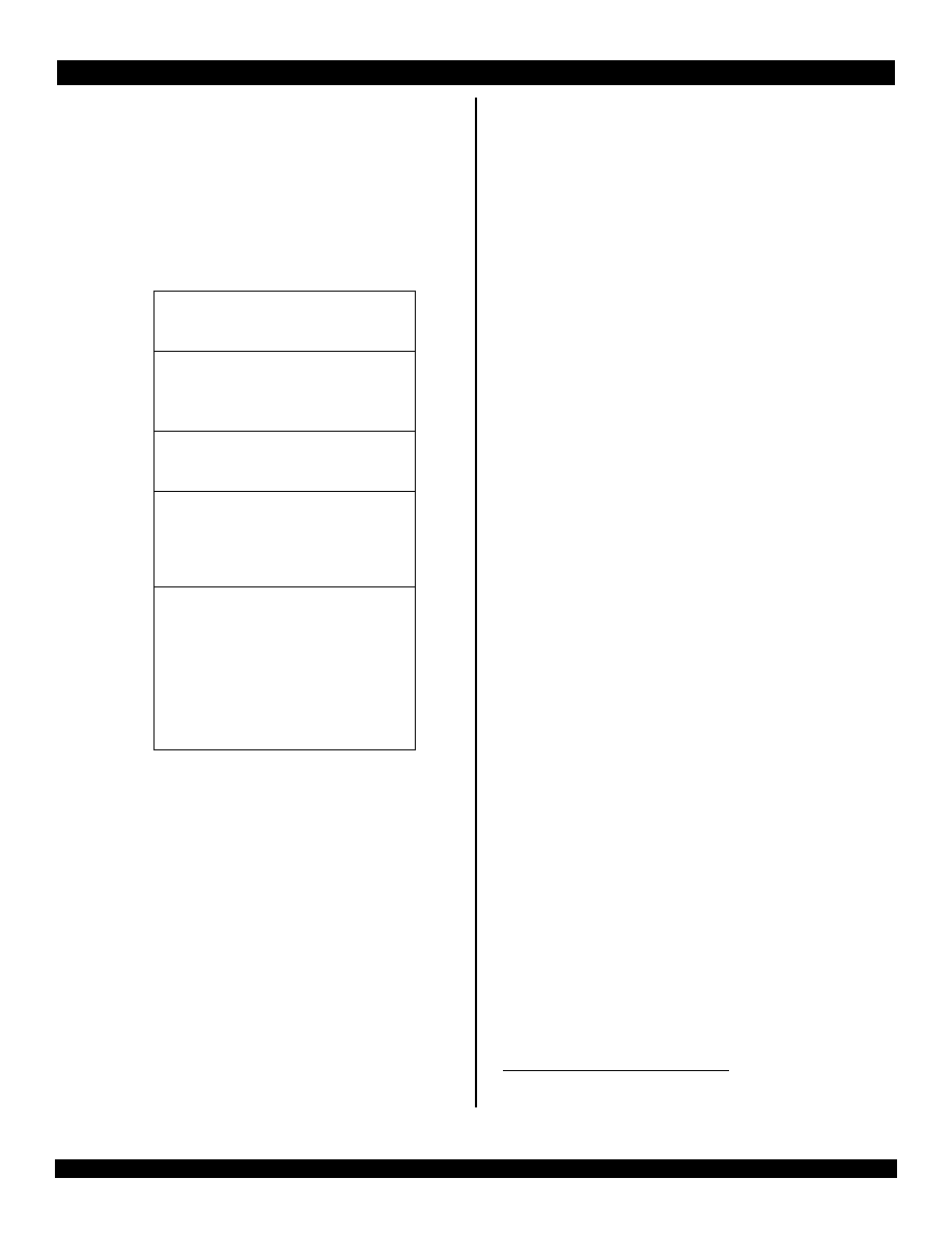
A secure user processing environment is provided through the user,
supervisor, and kernel operating modes of virtual addressing to
system software. Bits in a status register determine which of these
modes is used.
If configured for 64-bit virtual addressing, the virtual address space
layout becomes an upwardly compatible extension of the 32-bit virtual
address space layout. Figure 1 is an illustration of the address space
layout for the 32-bit virtual address operation.
The RC64474/RC64475's Memory Management Unit (MMU)
controls the virtual memory system's page mapping and consists of a
translation lookaside buffer (TLB) used for the virtual memory-mapping
subsystem.
This large, fully associative TLB maps 96 virtual pages to their
corresponding physical addresses. The TLB is organized as 48 pairs of
even-odd entries and maps a virtual address and address space identi-
fier into the large, 64GB physical address space. To assist in controlling
the amount of mapped space and the replacement characteristics of
various memory regions, two mechanisms are provided. First, the page
size can be configured on a per-entry basis, to map a page size of 4KB
to 16MB (in increments of 4x).
The second mechanism controls the replacement algorithm, when a
TLB miss occurs. A random replacement algorithm is provided to select
a TLB entry to be written with a new mapping; however, the processor
provides a mechanism whereby a system specific number of mappings
0xFFFFFFFF
0xE0000000
Kernel virtual address space
(kseg3)
Mapped, 0.5GB
0xDFFFFFFF
Supervisor virtual address space
(sseg)
Mapped, 0.5GB
0xC0000000
0xBFFFFFFF
0xA0000000
Uncached kernel physical address space
(kseg1)
Unmapped, 0.5GB
0x9FFFFFFF
0x80000000
Cached kernel physical address space
(kseg0)
Unmapped, 0.5GB
0x7FFFFFFF
0x00000000
User virtual address space
(useg)
Mapped, 2.0GB
Figure 1 Kernel Mode Virtual Addressing (32-bit Mode)
can be locked into the TLB and avoid being randomly replaced, which
facilitates the design of real-time systems, by allowing deterministic
access to critical software.
The TLB also contains information to control the cache coherency
protocol, and cache management algorithm for each page. However,
hardware-based cache coherency is not supported.
The RC64474 and RC64475 enhance IDT's entire RISCore4000
series through the implementation of features such as boundary scan, to
facilitate board level testing; enhanced support for SyncDRAM, to
simplify system implementation and improve performance.
The RC64474/475 processors offer a direct migration path for
designs based on IDT's RC4640/RC4650 processors
2
, through full pin
and socket compatibility. Also, full 64-bit-family software and bus-
protocol compatibility ensures the RC64474/475 access to a robust
development tools infrastructure, allowing quicker time to market.
Development Tools
Development Tools
Development Tools
Development Tools
An array of hardware and software tools is available to assist system
designers in the rapid development of RC64474/475 based systems.
This accessibility allows a wide variety of customers to take full advan-
tage of the device's high-performance features while addressing today's
aggressive time-to-market demands.
Cache Memory
Cache Memory
Cache Memory
Cache Memory
To keep the RC64474 and RC64475's high-performance pipeline full
and operating efficiently, on-chip instruction and data caches have been
incorporated. Each cache has its own data path and can be accessed in
the same single pipeline clock cycle.
The 16KB two-way set associative instruction cache (I-cache) is
virtually indexed, physically tagged, and word parity protected. Because
this cache is virtually indexed, the virtual-to-physical address translation
occurs in parallel with the cache access, further increasing performance
by allowing both operations to occur simultaneously. The instruction
cache provides a peak instruction bandwidth of 1000MB/sec at 250MHz.
The 16KB two-way set associative data cache (D-cache) is byte
parity protected and has a fixed 32-byte (eight words) line size. Its tag is
protected with a single parity bit. To allow simultaneous address transla-
tion and data cache access, the D-cache is virtually indexed and physi-
cally tagged. The data cache can provide 8 bytes each clock cycle, for a
peak bandwidth of 2GB/sec.
To lock critical sections of code and/or data into the caches for quick
access, a "cache locking" feature has been implemented. Once
enabled, a cache is said to be locked when a particular piece of code or
data is loaded into the cache and that cache location will not be selected
later for refill by other data. This feature locks a set (8KB) of Instructions
and/or Data.
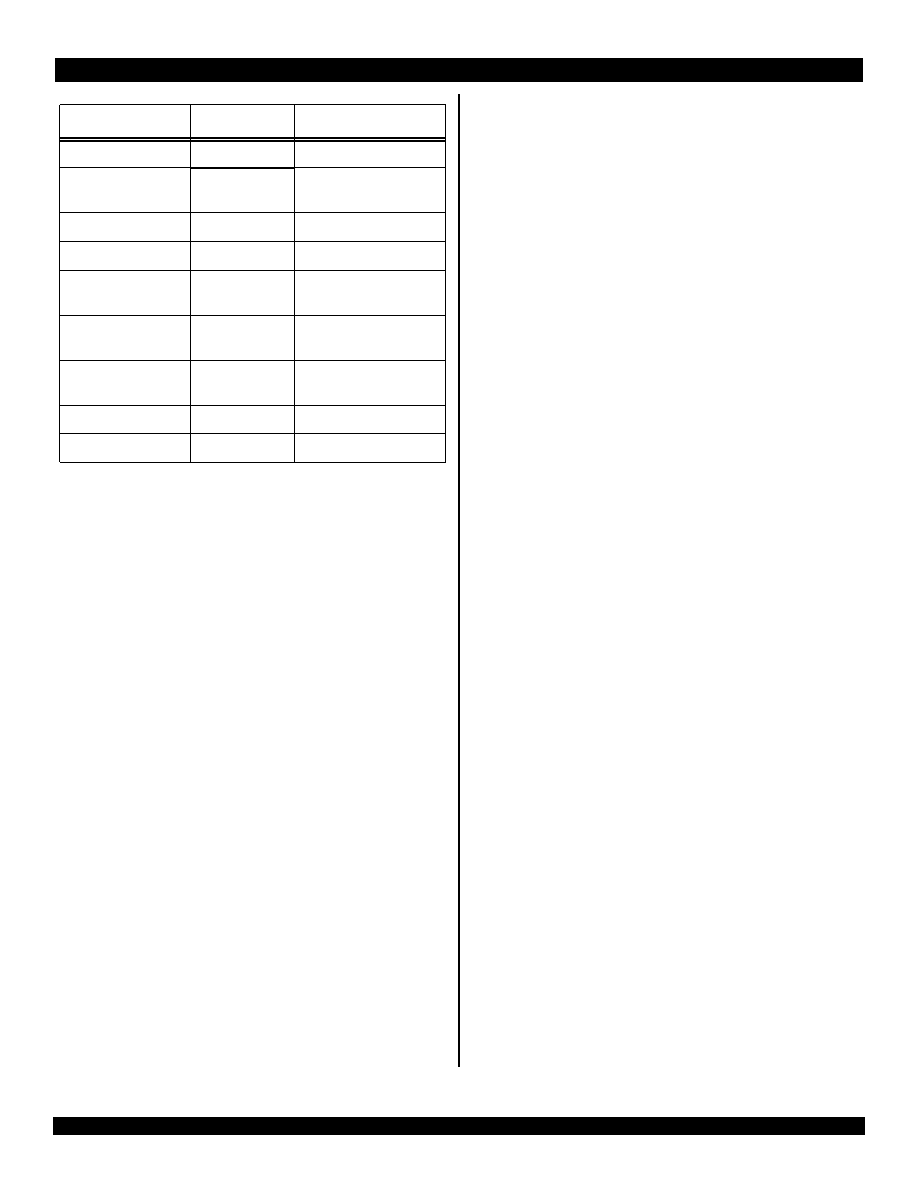
Table 2 lists the RC64474/475 Instruction and data cache attributes.
2.
To ensure socket compatibility, refer to Table 8 and Table 9 at back of data
sheet.
4 of 25
April 10, 2001
RC64474TM RC64475TM
Table 2 RC64474/RC64475 Instruction/Data Cache Attributes
System Interfaces
System Interfaces
System Interfaces
System Interfaces
The RC64475 supports a 64-bit system interface that is bus compat-
ible with the RC4650 and RC64575 system interface. The system inter-
face consists of a 64-bit Address/Data bus with 8 check bits and a 9-bit
command bus that is parity protected.
During 64-bit operation, RC64475 system address/data (SysAD)
transfers are protected with an 8-bit parity check bus, SysADC. When
initialized for 32-bit operation, the RC64475's SysAD can be viewed as a
32-bit multiplexed bus that is protected by 4 parity check bits.
The RC64474 supports a 32-bit system interface that is bus compat-
ible with the RC4640. During 32-bit operation, SysAD transfers are
performed on a 32-bit multiplexed bus (SysAD 31:0) that is protected by
4 parity check bits (SysADC 6:0).
Writes to external memory--whether they are cache miss write-
backs, stores to uncached or write-through addresses--use the on-chip
write buffer. The write buffer holds a maximum of four 64-bit addresses
and 64-bit data pairs. The entire buffer is used for a data cache write-
back and allows the processor to proceed in parallel with memory
updates.
Included in the system interface are six handshake signals:
RdRdy*, WrRdy*, ExtRqst*, Release*, ValidOut*, and ValidIn*; six inter-
rupt inputs, and a simple timing specification that is capable of trans-
ferring data between the processor and memory at a peak rate of
1000MB/sec. A boot-time selectable option to run the system interface
as 32-bits wide--using basically the same protocols as the 64-bit
system--is also supported.
Characteristics
Instruction
Data
Size
16KB
16KB
Organization
2-way set
associative
2-way set
associative
Line size
32B
32B
read unit
32-bits
64-bits
write policy
na
write-back, write-through
with or without write-allocate
Line transfer order
sub-block order,
for refill
sub-block order, for load
sequential order, for store
Miss restart
after transfer of:
entire line
miss word
Parity
per-word
per-byte
Cache locking
per set
per set
A boot-time mode control interface initializes fundamental
processor modes. The boot-time mode control interface is a serial inter-
face that operates at a very low frequency (MasterClock divided by
256). This low-frequency operation allows the initialization information to
be kept in a low-cost EPROM; alternatively, the twenty-or-so bits could
be generated by the system interface ASIC or a simple PAL. The boot-
time serial stream and configuration options are listed in Table 3.
The clocking interface allows the CPU to be easily mated with
external reference clocks. The CPU input clock is the bus reference
clock and can be between 25 and 125MHz. An on-chip phase-locked-
loop (PLL) generates the pipeline clock (PClock) through multiplication
of the system interface clock by values of 2,3,4,5,6,7 or 8, as defined at
system reset. This allows the pipeline clock to be implemented at a
significantly higher frequency than the system interface clock. The
RC64474/475 support single data (one to eight bytes) and 8-word block
transfers on the SysAD bus.
The RC64474/475 implement additional write protocols that
double the effective write bandwidth. The write re-issue has a repeat
rate of 2 cycles per write. Pipelined writes have the same 2-cycle per
write repeat rate, but can issue an additional write after WrRdy* de-
asserts.
Choosing a 32- or 64-bit wide system interface dictates whether a
cache line block transaction requires 4 double word data cycles or 8
single word cycles as well as whether a single data transfer--larger than
4 bytes--must be divided into two smaller transfers.
Board-level testing during Run-Time mode is facilitated through the
full JTAG boundary scan facility. Six pins--TDI, TDO, TMS, TCK, TRST*
and JTAG32*--have been incorporated to support the standard JTAG
interface.
System Enhancement
System Enhancement
System Enhancement
System Enhancement
To facilitate discrete interface to SDRAM, the RC64474/475 bus
interface is enhanced during write cycles with a programmable delay
that is inserted between the write address and the write data (for both
block and non-block writes).
The bus delay can be defined as 0 to 7 MasterClock cycles and is
activated and controlled through mode bit (17:15) settings selected
during the reset initialization sequence. The `000' setting provides the
same write operations timing protocol as the RC4640, RC4650, and
RC5000 processors.

5 of 25
April 10, 2001
RC64474TM RC64475TM
Serial
Bit
Description
Value & Mode Setting
255:18
Reserved
Must be 0
17:15
WAdrWData_Del
Write address to write data delay in Master-
Clock cycles.®
000
0 cycles
001
1 cycle
010
2 cycles
011
3 cycles
100
4 cycles
101
5 cycles
110
6 cycles
111
7 cycles
14:13
Drv_Out
output driver slew rate control. Bit 14 is MSB.
Affects only non-clock outputs.
Output driver strength:
10
100% strength (fastest)
11
83% strength
00
67% strength
01
50% strength (slowest)
12
System interface bus width
0
64-bit system interface
1
32-bit system interface
11
TmrIntEn
Disables the timer interrupt on Int*[5]
0
Enabled Timer Interrupt
1
Disabled Timer Interrupt
10:9
Non-block write
Selects non-block write type. Bit 10 is MSB.
00
RC4x00 compatible
01
Reserved
10
Pipelined writes
11
Write re-issue
7:5
Clock
Multiplier
MasterClock is multiplied internally to gener-
ate PClock
Clock multiplier:
0 Multiply by 2
1 Multiply by 3
2 Multiply by 4
3 Multiply by 5
4 Multiply by 6
5 Multiply by 7
6 Multiply by 8
7 Reserved
8
EndBit
Specifies byte ordering
0
Little endian
1
Big endian
4:1
Writeback data rate
System interface data rate for block writes
only: bit 4 is MSB
64-bit:
9:15 Reserved
8
dxxxdxxxdxxxdxxx
7
ddxxxxxxddxxxxxx
6
dxxdxxdxxdxx
5
ddxxxxddxxxx
4
ddxxxddxxx
3
dxdxdxdx
2
ddxxddxx
1
ddxddx
0
dddd
32-bit:
9:15 Reserved
8
wxxxwxxxwxxxwxxxwxxxwxxxwxxxwxxx
7
wwxxxxxxwwxxxxxxwwxxxxxxwwxxxxxx
6
wxxwxxwxxwxxwxxwxxwxxwxx
5
wwxxxxwwxxxxwwxxxxwwxxxx
4
wwxxxwwxxxwwxxxwwxxx
3
wxwxwxwxwxwxwxwx
2
wwxxwwxxwwxxwwxx
1
wwxwwxwwxwwx
0
Æ wwwwwwww
0
Reserved
Must be zero
Table 3 Boot-time Mode Stream
Document Outline