 | –≠–ª–µ–∫—Ç—Ä–æ–Ω–Ω—ã–π –∫–æ–º–ø–æ–Ω–µ–Ω—Ç: 79RV3041 | –°–∫–∞—á–∞—Ç—å:  PDF PDF  ZIP ZIP |
COMMERCIAL TEMPERATURE RANGE
MARCH 1996
©1996 Integrated Device Technology, Inc.
DSC-2905/5
IDT79R3041
TM
INTEGRATED RISController
TM
FOR
LOW-COST SYSTEMS
IDT79R3041
IDT79RV3041
FEATURES:
∑ Instruction set compatible with IDT79R3000A
and RISController Family MIPS RISC CPUs
∑ High level of integration minimizes system cost
-- RISC CPU
-- Multiply/divide unit
-- Instruction Cache
-- Data Cache
-- Programmable bus interface
-- Programmable port width support
∑ On-chip instruction and data caches
-- 2KB of Instruction Cache
-- 512B of Data Cache
∑ Flexible bus interface allows simple, low-cost designs
-- Superset pin-compatible with RISController
-- Adds programmable port width interface
(8-, 16-, and 32-bit memory sub-regions)
-- Adds programmable bus interface timing support
(Extended address hold, Bus turn around time,
Read/write masks)
∑ Double-frequency clock input
∑ 16.67MHz, 20MHz, 25MHz and 33MHz operation
∑ 20MIPS at 25MHz
∑ Low cost 84-pin PLCC packaging
∑ On-chip 4-deep write buffer eliminates memory write stalls
∑ On-chip 4-word read buffer supports burst or simple block
reads
∑ On-chip DMA arbiter
∑ On-chip 24-bit timer
∑ Boot from 8-bit, 16-bit, or 32-bit wide PROMs
∑ Pin- and software-compatible family includes R3041, R3051,
R3052
TM
, and R3081
TM
∑ Complete software support
-- Optimizing compilers
-- Real-time operating systems
-- Monitors/debuggers
-- Floating Point emulation software
-- Page Description Languages
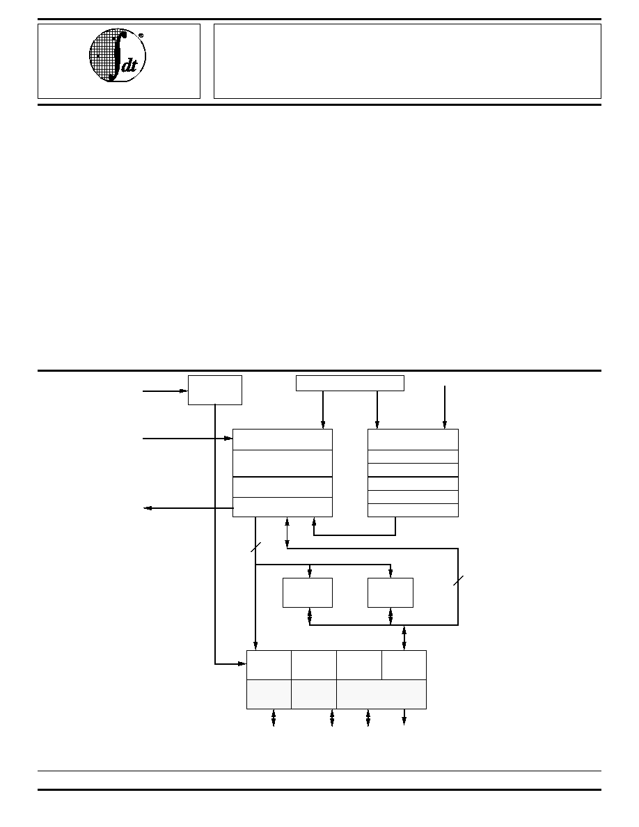
Figure 1. R3041 Block Diagram
Clock
Generator
Unit
Master Pipeline Control
System Control
Coprocessor
Integer
CPU Core
Exception/Control
Registers
Bus Interface
Registers
General Registers
(32 x 32)
ALU
Shifter
Mult/Div Unit
Address Adder
PC Control
Virtual Address
Data
Cache
512B
Instruction
Cache
2kB
Physical Address Bus
BIU
Control
DMA
Arbiter
4-deep
Read
Buffer
4-deep
Write
Buffer
ClkIn
Int(5:3)
,
SInt(2:0)
32
32
SBrCond(3:2)
Data Bus
Address/
Data
DMA
Ctrl
Rd
/
Wr
Ctrl
SysClk
PortSize
Register
Counter
Registers
TC
R3051 Superset
Bus Interface Unit
Data
Unpack
Unit
Data
Pack
Unit
Timing/ Interface
Control
2905 drw 01
1
Integrated Device Technology, Inc.
RISController, R3041, R3051, R3052, R3081, ORION, IDT/sim, and IDT/kit are trademarks, and the IDT logo is a registered trademark of Integrated Device Technology, Inc.
2
IDT79R3041 INTEGRATED RISController FOR LOW COST SYSTEMS
COMMERCIAL TEMPERATURE RANGE
Device
Instruction
Data
Floating
Bus
Name
Cache
Cache
Point
Options
R3051
4kB
2kB
Software Emulation
Mux'ed A/D
R3052
8kB
2kB
Software Emulation
Mux'ed A/D
R3071
16kB
4kB
On-chip Hardware
1/2 frequency bus option
R3081
or 8kB
or 8kB
R3041
2kB
512B
Software Emulation
8-, 16-, and 32-bit port width support
Programmable timing support
2905 tbl 01
INTRODUCTION
The IDT RISController family is a series of high-perfor-
mance 32-bit microprocessors featuring a high-level of inte-
gration, and targeted to high-performance but cost sensitive
embedded processing applications. The RISController family
is designed to bring the high-performance inherent in the
MIPS RISC architecture into low-cost, simplified, power sen-
sitive applications.
Thus, functional units have been integrated onto the CPU
core in order to reduce the total system cost, rather than to
increase the inherent performance of the integer engine.
Nevertheless, the RISController family is able to offer 35MIPS
of integer performance at 40MHz without requiring external
SRAM or caches.
Further, the RISController family brings dramatic power
reduction to these embedded applications, allowing the use of
low-cost packaging. Thus, the RISController family allows
customer applications to bring maximum performance at
minimum cost.
The R3041 extends the range of price/performance achiev-
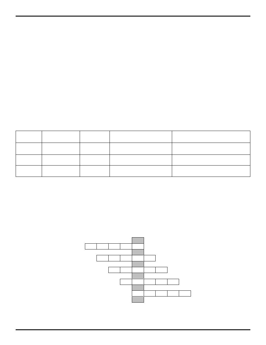
Table 1. Pin-Compatible RISController Family
Figure 2. RISController Family 5-Stage Pipeline
CPU Core
The CPU core is a full 32-bit RISC integer execution
engine, capable of sustaining close to a single cycle execution
rate. The CPU core contains a five stage pipeline, and 32
orthogonal 32-bit registers. The RISController family imple-
ments the MIPS-I Instruction Set Architecture (ISA). In fact,
the execution engine of the R3041 is the same as the
execution engine of the R3000A. Thus, the R3041 is binary
compatible with those CPU engines, as well as compatible
with other members of the RISController family.
able with the RISController family, by dramatically lowering
the cost of using the MIPS architecture. The R3041 is de-
signed to achieve minimal system and components cost, yet
maintain the high-performance inherent in the MIPS architec-
ture. The R3041 also maintains pin and software compatibility
with the RISController and R3081.
The RISController family offers a variety of price/perfor-
mance features in a pin-compatible, software compatible
family. Table 1 provides an overview of the current members
of the RISController family. Note that the R3051, R3052, and
R3081 are also available in pin-compatible versions that
include a full-function memory management unit, including
64-entry TLB. The R3051/2 and R3081 are described in
separate manuals and data sheets.
Figure 1 shows a block level representation of the func-
tional units within the R3041. The R3041 can be viewed as the
embodiment of a discrete solution built around the R3000A.
By integrating this functionality on a single chip, dramatic cost
and power reductions are achieved.
An overview of these blocks is presented here, followed
with detailed information on each block.
IF
Current
CPU
Cycle
I#1
ALU
RD
MEM
WB
IF
I#2
ALU
RD
MEM
WB
IF
I#3
ALU
RD
MEM
WB
IF
I#4
ALU
RD
MEM
WB
IF
I#5
ALU
RD
MEM
WB
2905 drw 02
The execution engine of the RISController family uses a
five-stage pipeline to achieve close to single cycle execution.
A new instruction can be started in every clock cycle; the
execution engine actually processes five instructions concur-
rently (in various pipeline stages). The five parts of the pipeline
are the Instruction Fetch, Read register, ALU execution,
Memory, and Write Back stages. Figure 2 shows the
concurrency achieved by the RISController family pipeline.
3
IDT79R3041 INTEGRATED RISController FOR LOW COST SYSTEMS
COMMERCIAL TEMPERATURE RANGE
System Control Co-Processor
The R3041 also integrates on-chip a System Control Co-
processor, CP0. CP0 manages the exception handling capa-
bility of the R3041, the virtual to physical address mapping of
the R3041, and the programmable bus interface capabilities
of the R3041. These topics are discussed in subsequent
sections.
The R3041 does not include the optional TLB found in other
members of the RISController family, but instead performs the
same virtual to physical address mapping of the base version
of the RISController family. These devices still support
distinct kernel and user mode operation, but do not require
page management software or an on-chip TLB, leading to a
simpler software model and a lower-cost processor.
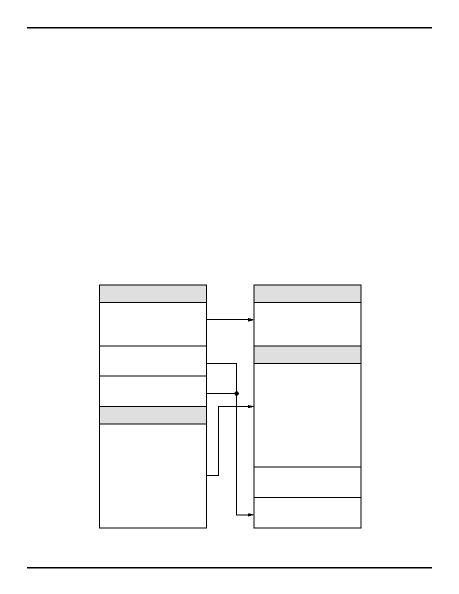
The memory mapping used by these devices is illustrated
in Figure 3. Note that the reserved address spaces shown are
for compatibility with future family members; in the current
family members, references to these addresses are trans-
lated in the same fashion as their respective segments, with
no traps or exceptions taken.
When using the base versions of the architecture, the
system designer can implement a distinction between the
user tasks and the kernel tasks, without having to execute
page management software. This distinction can take the
form of physical memory protection, accomplished by ad-
dress decoding, or in other system specific forms. In systems
which do not wish to implement memory protection, and wish
to have the kernel and user tasks operate out of a single
unified memory space, upper address lines can be ignored by
the address decoder, and thus all references will be seen in
the lower gigabyte of the physical address space.
The R3041 adds additional resources into the on-chip CP0.
These resources are detailed in the R3041 User's Manual.
They allow kernel software to directly control activity of the
processor internal resources and bus interface, and include:
∑ Cache Configuration Register: This register controls the
data cache block size and miss refill algorithm.
∑ Bus Control Register: This register controls the behavior
of the various bus interface signals.
∑ Count and Compare Registers: Together, these two
registers implement a programmable 24-bit timer, which
can be used for DRAM refresh or as a general purpose
timer.
∑ Port Size Control Register: This register allows the kernel
to indicate the port width of reads and writes to various sub-
regions of the physical address space. Thus, the R3041 can
interface directly with 8-, 16-, and 32-bit memory ports,
including a mix of sizes, for both instruction and data
references, without requiring additional external logic.
Figure 3. Virtual to Physical Mapping of Base Architecture Versions
VIRTUAL
PHYSICAL
2905 drw 03
Kernel Cached
(kseg2)
Kernel Uncached
(kseg1)
Kernel Cached
(kseg0)
Kernel/User
Cached
(kuseg)
Kernel Cached
Tasks
1023 MB
Kernel/User
Cached
Tasks
2047 MB
Inaccessible
512 MB
Kernel Boot
and I/O
512 MB
0xfff00000
0xc0000000
0xa0000000
0x00000000
0xffffffff
0x80000000
0x7fffffff
0x7ff00000
0x7fefffff
0x9fffffff
0xbfffffff
0xffefffff
User Reserved
1MB
Kernel Reserved
1MB
0xfff00000
0xc0000000
0xbff00000
0x00000000
0xffffffff
0x40000000
0x3fffffff
0x20000000
0x1fffffff
0xbfefffff
0xbfffffff
0xffefffff
Kernel Reserved
1MB
User Reserved
1MB

4
IDT79R3041 INTEGRATED RISController FOR LOW COST SYSTEMS
COMMERCIAL TEMPERATURE RANGE
Clock Generation Unit
The R3041 is driven from a single 2x frequency input clock,
capable of operating in a range of 40%-60% duty cycle. On-
chip, the clock generator unit is responsible for managing the
interaction of the CPU core, caches, and bus interface. The
clock generator unit replaces the external delay line required
in R3000A based applications.
Instruction Cache
The R3041 integrates 2kB of on-chip Instruction Cache,
organized with a line size of 16 bytes (four 32-bit entries) a nd
is direct mapped. This relatively large cache substantially
contributes to the performance inherent in the R3041, and
allows systems based on the R3041 to achieve high-perfor-
mance even from low-cost memory systems. The cache is
implemented as a direct mapped cache, and is capable of
caching instructions from anywhere within the 4GB physical
address space. The cache is implemented using physical
addresses and physical tags (rather than virtual addresses or
tags), and thus does not require flushing on context switch.
Data Cache
The R3041 incorporates an on-chip data cache of 512B,
organized as a line size of 4 bytes (one word) and is direct
mapped. This relatively large data cache contributes substan-
tially to the performance inherent in the RISController family.
As with the instruction cache, the data cache is implemented
as a direct mapped physical address cache. The cache is
capable of mapping any word within the 4GB physical address
space.
The data cache is implemented as a write through cache,
to insure that main memory is always consistent with the
internal cache. In order to minimize processor stalls due to
data write operations, the bus interface unit incorporates a 4-
deep write buffer which captures address and data at the
processor execution rate, allowing it to be retired to main
memory at a much slower rate without impacting system
performance.
Bus Interface Unit
The RISController family uses its large internal caches to
provide the majority of the bandwidth requirements of the
execution engine, and thus can utilize a simple bus interface
connected to slow memory devices.
The RISController family bus interface utilizes a 32-bit
address and data bus multiplexed onto a single set of pins.
The bus interface unit also provides an ALE (Address Latch
Enable) output signal to de-multiplex the A/D bus, and simple
handshake signals to process CPU read and write requests.
In addition to the read and write interface, the R3041 incorpo-
rates a DMA arbiter, to allow an external master to control the
external bus.
The R3041 augments the basic RISController bus interface
capability by adding the ability to directly interface with varying
memory port widths, for instructions or data. For example, the
R3041 can be used in a system with an 8-bit boot PROM, 16-
bit font/program cartridges, and 32-bit main memory, trans-
parently to software, and without requiring external data
packing, rotation, and unpacking.
In addition, the R3041 incorporates the ability to change
some of the interface timing of the bus. These features can be
used to eliminate external data buffers and take advantage of
lower speed and lower cost interface components.
One of the bus interface options is the Extended Address
Hold mode which adds 1/2 clock of extra address hold time
from ALE falling. This allows easier interfacing to FPGAs and
ASICs.
The R3041 incorporates a 4-deep write buffer to decouple
the speed of the execution engine from the speed of the
memory system. The write buffers capture and FIFO proces-
sor address and data information in store operations, and
present it to the bus interface as write transactions at the rate
the memory system can accommodate. During main memory
writes, the R3041 can break a large datum (e.g. 32-bit word)
into a series of smaller transactions (e.g. bytes), according to
the width of the memory port being written. This operation is
transparent to the software which initiated the store, insuring
that the same software can run in true 32-bit memory systems.
The RISController family read interface performs both
single word reads and quad word reads. Single word reads
work with a simple handshake, and quad word reads can
either utilize the simple handshake (in lower performance,
simple systems) or utilize a tighter timing mode when the
memory system can burst data at the processor clock rate.
Thus, the system designer can choose to use page or static
column mode DRAMs (and possibly use interleaving, if de-
sired, in high-performance systems), or even to use simpler
SRAM techniques to reduce complexity.
In order to accommodate slower quad word reads, the
RISController family incorporates a 4-deep read buffer FIFO,
so that the external interface can queue up data within the
processor before releasing it to perform a burst fill of the
internal caches.
In addition, the R3041 can perform on-chip data packing
when performing large datum reads (e.g., quad words) from
narrower memory systems (e.g., 16-bits). Once again, this
operation is transparent to the actual software, simplifying
migration of software to higher performance (true 32-bit)
systems, and simplifying field upgrades to wider memory.
Since this capability works for either instruction or data reads,
using 8-, 16-, or 32-bit boot PROMs is easily supported by the
5
IDT79R3041 INTEGRATED RISController FOR LOW COST SYSTEMS
COMMERCIAL TEMPERATURE RANGE
R3041.
SYSTEM USAGE
The IDT RISController family is specifically designed to
easily connect to low-cost memory systems. Typical low-cost
memory systems use inexpensive EPROMs, DRAMs, and
application specific peripherals.
Figure 4 shows some of the flexibility inherent in the R3041.
In this example system, which is typical of a laser printer, a 32-
bit PROM interface is used due to the size of the PDL
interpreter. An embedded system can optionally use an 8-bit
Figure 4. Typical R3041-Based Application
boot PROM instead. A 16-bit font/program cartridge interface
is provided for add-in cards. A 16-bit DRAM interface is used
for a low-cost page frame buffer. In this system example, a
field or manufacturing upgrade to a 32-bit page frame buffer
is supported by the boot software and DRAM controller.
Embedded systems may optionally substitute SRAMs for the
DRAMs. Finally various 8/16/32-bit I/O ports such as RS-232/
422, SCSI, and LAN as well as the laser printer engine
interface are supported. Such a system features a very low
entry price, with a range of field upgrade options including the
ability to upgrade to a more powerful member of the
RISController family.
ClkIn
IDT R3041
RISController
Address/
Data
Control
EPROM and
I/O Controller
DRAM
Controller
16-bit
DRAM
16-bit
Add-on
DRAM
32-bit
EPROM
16-bit
Font
Cartridge
I/O
R3051
Local Bus
2905 drw 04