 | –≠–ª–µ–∫—Ç—Ä–æ–Ω–Ω—ã–π –∫–æ–º–ø–æ–Ω–µ–Ω—Ç: 79RV3081 | –°–∫–∞—á–∞—Ç—å:  PDF PDF  ZIP ZIP |
5.5
1
IDT79R3081 RISController
MILITARY AND COMMERCIAL TEMPERATURE RANGES
MILITARY AND COMMERCIAL TEMPERATURE RANGES OCTOBER 2001
©
2001 Integrated Device Technology, Inc.
5.5
DSC-9064/5
IDT 79R3081
TM
, 79R3081E
IDT 79RV3081, 79RV3081E
IDT79R3081
RISController
TM
with FPA
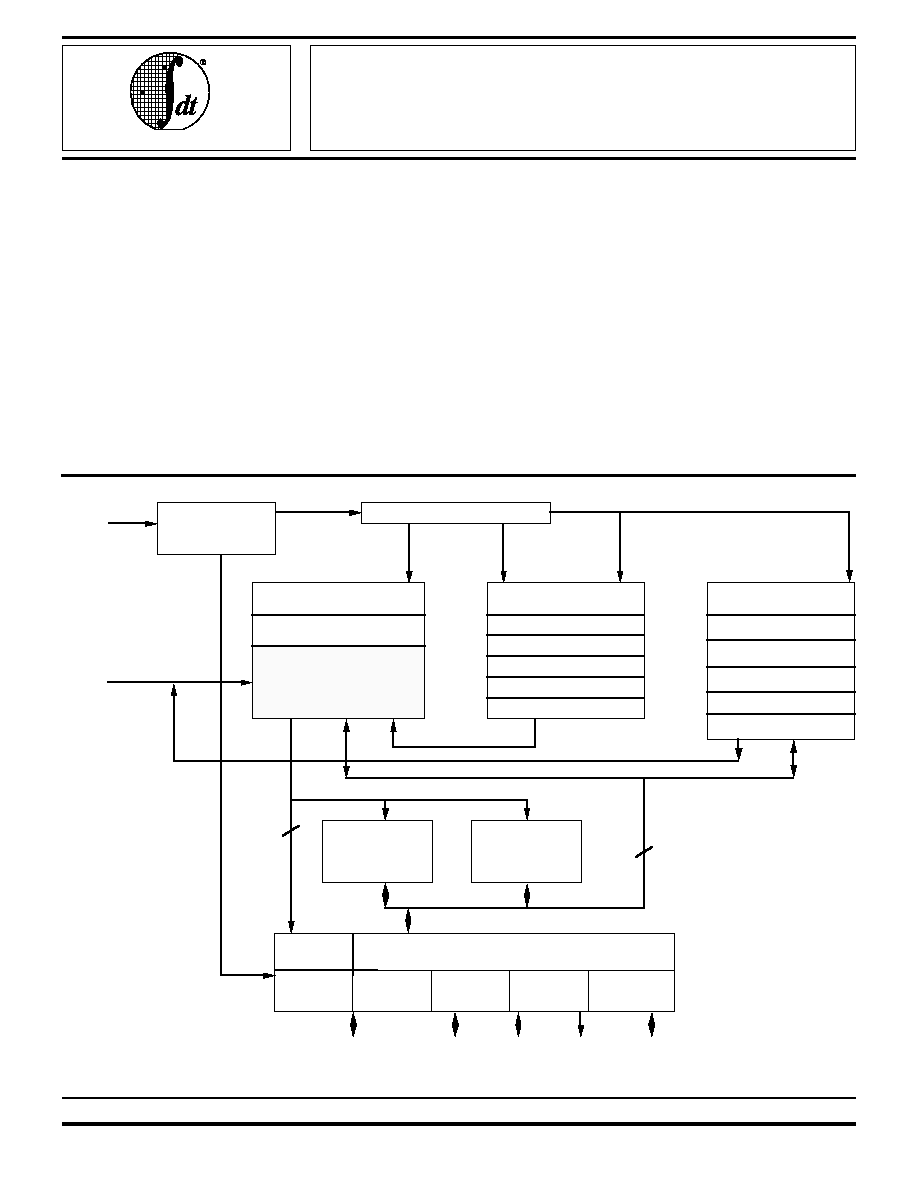
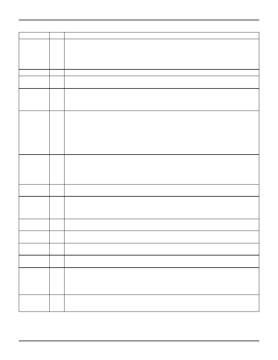
R3081 BLOCK DIAGRAM
Clock Generator
Unit/Clock Doubler
Master Pipeline Control
System Control
Coprocessor
(CP0)
Integer
CPU Core
Exception/Control
Registers
Memory Management
Registers
Translation
Lookaside Buffer
(64 entries)
General Registers
(32 x 32)
ALU
Shifter
Mult/Div Unit
Address Adder
PC Control
Virtual Address
Configurable
Data
Cache
(4kB/8kB)
Configurable
Instruction
Cache
(16kB/8kB)
Physical Address Bus
BIU
Control
DMA
Arbiter
4-deep
Write
Buffer
ClkIn
Int(5:0)
32
36
BrCond(3:2,0)
Data Bus
R3051 Superset Bus Interface Unit
Address/
Data
DMA
Ctrl
Rd/Wr
Ctrl
SysClk
Register Unit
(16 x 64)
Exponent Unit
Add Unit
Divide Unit
Multiply Unit
Floating Point
Coprocessor
(CP1)
Coherency
Logic
Invalidate
Control
Exception/Control
Data Bus
FP Interrupt
Parity
Generator
4-deep
Read
Buffer
2889 drw 01
The IDT logo is a registered trademark, and RISController, R3041, R3051, R3052, R3071, R3081, R3720, R4400, R4600, IDT/kit, and IDT/sim are trademarks of Integrated Device Technology, Inc.
FEATURES
∑ Instruction set compatible with IDT79R3000A, R3041,
R3051, and R3071 RISC CPUs
∑ High level of integration minimizes system cost
-- R3000A Compatible CPU
-- R3010A Compatible Floating Point Accelerator
-- Optional R3000A compatible MMU
-- Large Instruction Cache
-- Large Data Cache
-- Read/Write Buffers
∑ 43VUPS at 50MHz
-- 13MFlops
∑ Flexible bus interface allows simple, low cost designs
∑ Optional 1x or 2x clock input
∑ 20 through 50MHz operation
∑ "V" version operates at 3.3V
∑ 50MHz at 1x clock input and 1/2 bus frequency only
∑ Large on-chip caches with user configurability
-- 16kB Instruction Cache, 4kB Data Cache
-- Dynamically configurable to 8kB Instruction Cache,
8kB Data Cache
-- Parity protection over data and tag fields
∑ Low cost 84-pin packaging
∑ Superset pin- and software-compatible with R3051, R3071
∑ Multiplexed bus interface with support for low-cost, low-
speed memory systems with a high-speed CPU
∑ On-chip 4-deep write buffer eliminates memory write stalls
∑ On-chip 4-deep read buffer supports burst or simple block
reads
∑ On-chip DMA arbiter
∑ Hardware-based Cache Coherency Support
∑ Programmable power reduction mode
∑ Bus Interface can operate at half-processor frequency
Integrated Device Technology, Inc.

5.5
2
IDT79R3081 RISController
MILITARY AND COMMERCIAL TEMPERATURE RANGES
∑
The R3051, which incorporates 4kB of instruction cache
and 2kB of data cache, but omits the TLB, and instead uses
a simpler virtual to physical address mapping.
∑
The R3081E, which incorporates a 16kB instruction cache,
a 4kB data cache, and full function memory management
unit (MMU) including 64-entry fully associative Translation
Lookaside Buffer (TLB). The cache on the R3081E is user
configurable to an 8kB Instruction Cache and 8kB Data
Cache.
∑
The R3081, which incorporates a 16kB instruction cache,
a 4kB data cache, but uses the simpler memory mapping
of the R3051/52, and thus omits the TLB. The cache on the
R3081 is user configurable to an 8kB Instruction Cache and
8kB Data Cache.
Figure 1 shows a block level representation of the functional
units within the R3081E. The R3081E could be viewed as the
embodiment of a discrete solution built around the R3000A
and R3010A. However, by integrating this functionality on a
single chip, dramatic cost and power reductions are achieved.
CPU Core
The CPU core is a full 32-bit RISC integer execution
engine, capable of sustaining close to single cycle execution.
The CPU core contains a five stage pipeline, and 32 orthogonal
32-bit registers. The R3081 uses the same basic integer
execution core as the entire R3051 family, which is the
R3000A implementation of the MIPS instruction set. Thus, the
R3081 family is binary compatible with the R3051, R3052,
R3000A, R3001, and R3500 CPUs. In addition, the R4000
represents an upwardly software compatible migration path to
still higher levels of performance.
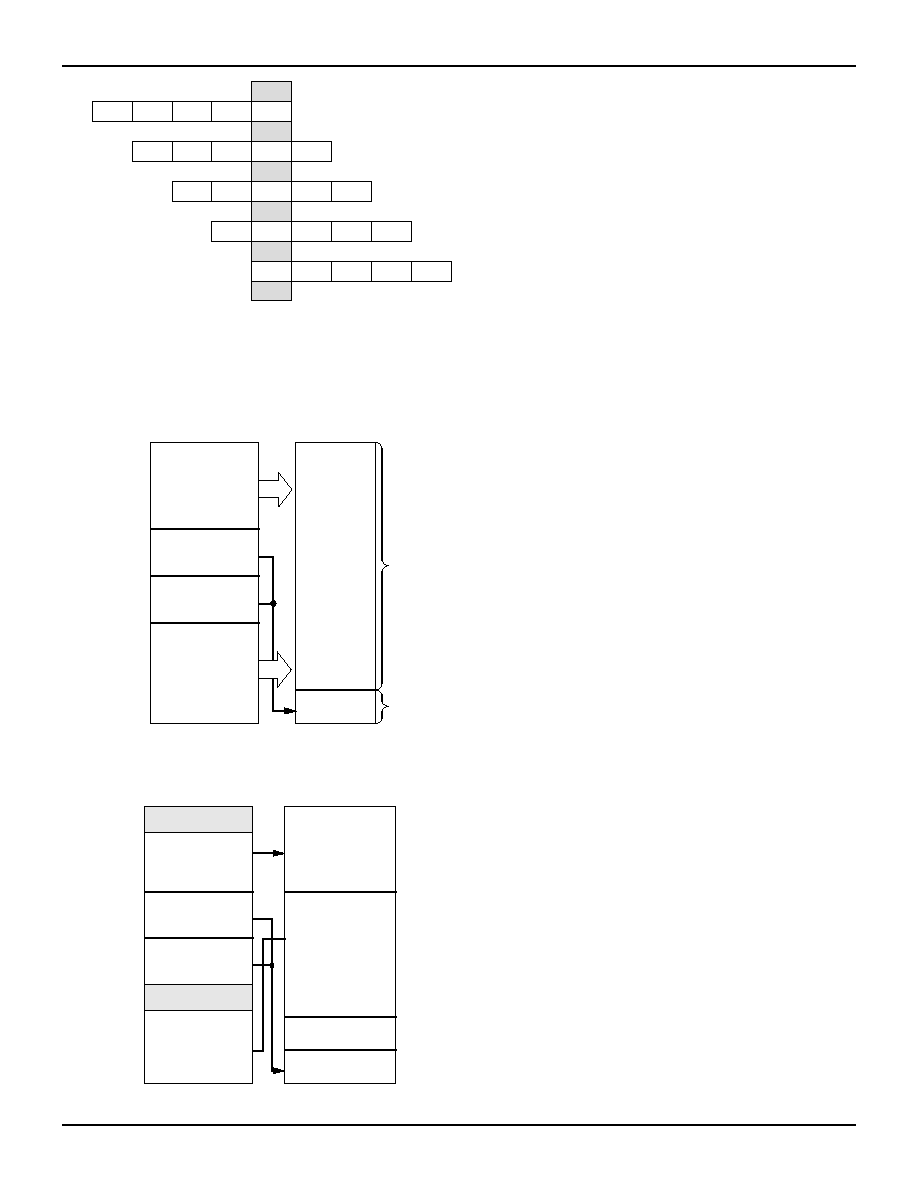
The execution engine in the R3081 uses a five-stage
pipeline to achieve near single-cycle instruction execution
rates. A new instruction can be initiated in each clock cycle;
the execution engine actually processes five instructions
concurrently (in various pipeline stages). Figure 2 shows the
concurrency achieved in the R3081 execution pipeline.
System Control Co-Processor
The R3081 family also integrates on-chip the System
Control Co-processor, CP0. CP0 manages both the exception
handling capability of the R3081, as well as the virtual to
physical address mapping.
As with the R3051 and R3052, the R3081 offers two
versions of memory management and virtual to physical
address mapping: the extended architecture versions, the
R3051E, R3052E, and R3081E, incorporate the same MMU
as the R3000A. These versions contain a fully associative 64-
entry TLB which maps 4kB virtual pages into the physical
address space. The virtual to physical mapping thus includes
kernel segments which are hard-mapped to physical
addresses, and kernel and user segments which are mapped
page by page by the TLB into anywhere in the 4GB physical
address space. In this TLB, 8 pages can be "locked" by the
kernel to insure deterministic response in real-time applications.
Figure 3 illustrates the virtual to physical mapping found in the
R3081E.
INTRODUCTION
The IDT R3051 family is a series of high-performance 32-
bit microprocessors featuring a high-level of integration, and
targeted to high-performance but cost sensitive processing
applications. The R3051 family is designed to bring the high-
performance inherent in the MIPS RISC architecture into
low-cost, simplified, power sensitive applications.
Thus, functional units have been integrated onto the CPU
core in order to reduce the total system cost, rather than to
increase the inherent performance of the integer engine.
Nevertheless, the R3051 family is able to offer 43VUPS
performance at 50MHz without requiring external SRAM or
caches.
The R3081 extends the capabilities of the R3051 family, by
integrating additional resources into the same pin-out. The
R3081 thus extends the range of applications addressed by
the R3051 family, and allows designers to implement a single,
base system and software set capable of accepting a wide
variety of CPUs, according to the price/performance goals of
the end system.
In addition to the embedded applications served by the
R3051 family, the R3081 allows low-cost, entry level computer
systems to be constructed. These systems will offer many
times the performance of traditional PC systems, yet cost
approximately the same. The R3081 is able to run any
standard R3000A operation system, including ACE UNIX.
Thus, the R3081 can be used to build a low-cost ARC
compliant system, further widening the range of performance
solutions of the ACE Initiative.
An overview of this device, and quantitative electrical
parameters and mechanical data, is found in this data sheet;
consult the
"R3081 Family Hardware User's Guide"
for a
complete description of this processor.
DEVICE OVERVIEW
As part of the R3051 family, the R3081 extends the offering
of a wide range of functionality in a compatible interface. The
R3051 family allows the system designer to implement a
single base system, and utilize interface-compatible processors
of various complexity to achieve the price-performance goals
of the particular end system.
Differences among the various family members pertain to
the on-chip resources of the processor. Current family members
include:
∑
The R3052E, which incorporates an 8kB instruction cache,
a 2kB data cache, and full function memory management
unit (MMU) including 64-entry fully associative Translation
Lookaside Buffer (TLB).
∑
The R3052, which also incorporates an 8kB instruction
cache and 2kB data cache, but does not include the TLB,
and instead uses a simpler virtual to physical address
mapping.
∑
The R3051E, which incorporates 4kB of instruction cache
and 2kB of data cache, along with the full function MMU/
TLB of the R3000A.
5.5
3
IDT79R3081 RISController
MILITARY AND COMMERCIAL TEMPERATURE RANGES
The extended architecture versions of the R3051 family
(the R3051E, R3052E, and R3081E) allow the system designer
to implement kernel software which dynamically manages
user task utilization of system resources, and also allows the
Kernel to protect certain resources from user tasks. These
capabilities are important in general computing applications
such as ARC computers, and are also important in a variety of
embedded applications, from process control (where protection
may be important) to X-Window display systems (where
virtual memory management can be used). The MMU can
also be used to simplify system debug.
R3051 family base versions (the R3051, R3052, and R3081)
remove the TLB and institute a fixed address mapping for the
various segments of the virtual address space. These devices
still support distinct kernel and user mode operation, but do
not require page management software, leading to a simpler
software model. The memory mapping used by these devices
is shown in Figure 4. Note that the reserved spaces are for
compatiblity with future family members, which may map on-
chip resources to these addresses. References to these
addresses in the R3081 will be translated in the same fashion
as the rest of their respective segments, with no traps or
exceptions signalled.
When using the base versions of the architecture, the
system designer can implement a distinction between the
user tasks and the kernel tasks, without having to implement
page management software. This distinction can be
implemented by decoding the output physical address. In
systems which do not need memory protection, and wish to
have the kernel and user tasks operate out of the same
memory space, high-order address lines can be ignored by
the address decoder, and thus all references will be seen in
the lower gigabyte of the physical address space.
Floating Point Co-Processor
The R3081 also integrates an R3010A compatible floating
point accelerator on-chip. The FPA is a high-performance co-
processor (co-processor 1 to the CPU) providing separate
add, multiply, and divide functional units for single and double
precision floating point arithmetic. The floating point accelerator
features low latency operations, and autonomous functional
units which allow differing types of floating point operations to
function concurrently with integer operations. The R3010A
appears to the software programmer as a simple extension of
the integer execution unit, with 16 dedicated 64-bit floating
point registers (software references these as 32 32-bit registers
when performing loads or stores). Figure 5 illustrates the
functional block diagram of the on-chip FPA.
Clock Generator Unit
The R3081 is driven from a single input clock which can be
either at the processor rated speed, or at twice that speed. On-
chip, the clock generator unit is responsible for managing the
interaction of the CPU core, caches, and bus interface. The
R3081 includes an on-chip clock doubler to provide higher
frequency signals to the internal execution core; if 1x clock
mode is selected, the clock doubler will internally convert it to
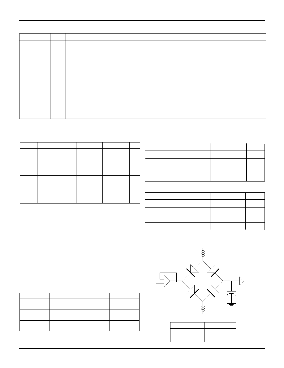
Figure 4. Virtual to Physical Mapping of Base Architecture Versions
1MB Kernel Rsvd
Kernel Cacheable
Tasks
Kernel/User
Cacheable
Tasks
Inaccessible
Kernel Boot
and I/O
0xffffffff
0xc0000000
0xa0000000
0x80000000
0x00000000
1024 MB
2048 MB
512 MB
512 MB
VIRTUAL
PHYSICAL
Kernel Cached
(kseg2)
Kernel Uncached
(kseg1)
Kernel Cached
(kseg0)
User
Cached
(kuseg)
1MB User Rsvd
2889 drw 04
Figure 3. Virtual to Physical Mapping of Extended Architecture
Versions
Kernel Mapped
(kseg2)
Kernel Uncached
(kseg1)
Kernel Cached
(kseg0)
User Mapped
Cacheable
(kuseg)
Physical
Memory
Memory
0xffffffff
0xc0000000
0xa0000000
0x80000000
0x00000000
3548MB
512 MB
Any
Any
VIRTUAL
PHYSICAL
2889 drw 03
Figure 2. R3081 5-Stage Pipeline
IF
Current
CPU
Cycle
I#1
ALU
RD
MEM
WB
IF
I#2
ALU
RD
MEM
WB
IF
I#3
ALU
RD
MEM
WB
IF
I#4
ALU
RD
MEM
WB
IF
I#5
ALU
RD
MEM
WB
2889 drw 02
5.5
4
IDT79R3081 RISController
MILITARY AND COMMERCIAL TEMPERATURE RANGES
a double frequency clock. The 2x clock mode is provided for
compatiblity with the R3051. The clock generator unit replaces
the external delay line required in R3000A based applications.
Instruction Cache
The R3081 implements a 16kB Instruction Cache. The
system may choose to repartition the on-chip caches, so that
the instruction cache is reduced to 8kB but the data cache is
increased to 8kB. The instruction cache is organized with a
line size of 16bytes (four entries). This large cache achieves
hit rates in excess of 98% in most applications, and substantially
contributes to the performance inherent in the R3081. The
cache is implemented as a direct mapped cache, and is
capable of caching instructions from anywhere within the 4GB
physical address space. The cache is implemented using
physical addresses (rather than virtual addresses), and thus
does not require flushing on context switch.
The instruction cache is parity protected over the instruction
word and tag fields. Parity is generated by the read buffer
during cache refill; during cache references, the parity is
checked, and in the case of a parity error, a cache miss is
processed.
Data Cache
The R3081 incorporates an on-chip data cache of 4kB,
organized as a line size of 4 bytes (one word). The R3081
allows the system to reconfigure the on-chip cache from the
default 16kB I-Cache/4kB D-Cache to 8kB of Instruction and
8kB of Data caches.
The relatively large data cache achieves hit rates in excess
of 95% in most applications, and contributes substantially to
the performance inherent in the R3081. As with the instruction
cache, the data cache is implemented as a direct mapped
physical address cache. The cache is capable of mapping any
word within the 4GB physical address space.
The data cache is implemented as a write-through cache,
to insure that main memory is always consistent with the
internal cache. In order to minimize processor stalls due to
data write operations, the bus interface unit incorporates a 4-
deep write buffer which captures address and data at the
processor execution rate, allowing it to be retired to main
memory at a much slower rate without impacting system
performance. Further, support has been provided to allow
hardware based data cache coherency in a multi-master
environment, such as one utilizing DMA from I/O to memory.
The data cache is parity protected over the data and tag
fields. Parity is generated by the read buffer during cache refill;
during cache references, the parity is checked, and in the case
of a parity error, a cache miss is processed.
Bus Interface Unit
The R3081 uses its large internal caches to provide the
majority of the bandwidth requirements of the execution
engine, and thus can utilize a simple bus interface connected
to slower memory devices. Alternately, a high-performance,
low-cost secondary cache can be implemented, allowing the
processor to increase performance in systems where bus
bandwidth is a performance limitation.
As part of the R3051 family, the R3081 bus interface utilizes
a 32-bit address and data bus multiplexed onto a single set of
pins. The bus interface unit also provides an ALE (Address
Latch Enable) output signal to de-multiplex the A/D bus, and
Figure 5. FPA Functional Block Diagram
Cache
Data
Data Bus
Instructions
Operands
Condition
Codes
Exponent Part
Fraction
Register Unit (16 X 64)
(32)
(32)
Control Unit
and Clocks
(11)
(11)
(11)
(53)
(53)
(53)
(53)
(53)
(56)
(53)
(53)
(56)
A
B
Result
Result
Exponent
Unit
A
B
Add Unit
Round
Result
A
B
Result
A
B
Divide Unit
Multiply Unit
2889 drw 05

5.5
5
IDT79R3081 RISController
MILITARY AND COMMERCIAL TEMPERATURE RANGES
simple handshake signals to process CPU read and write
requests. In addition to the read and write interface, the R3051
family incorporates a DMA arbiter, to allow an external master
to control the external bus.
The R3081 also supports hardware based cache coherency
during DMA writes. The R3081 can invalidate a specified line
of data cache, or in fact can perform burst invalidations during
burst DMA writes.
The R3081 incorporates a 4-deep write buffer to decouple
the speed of the execution engine from the speed of the
memory system. The write buffers capture and FIFO processor
address and data information in store operations, and present
it to the bus interface as write transactions at the rate the
memory system can accommodate.
The R3081 read interface performs both single datum
reads and quad word reads. Single reads work with a simple
handshake, and quad word reads can either utilize the simple
handshake (in lower performance, simple systems) or utilize
a tighter timing mode when the memory system can burst data
at the processor clock rate. Thus, the system designer can
choose to utilize page or nibble mode DRAMs (and possibly
use interleaving, if desired, in high-performance systems), or
use simpler techniques to reduce complexity.
In order to accommodate slower quad word reads, the
R3081 incorporates a 4-deep read buffer FIFO, so that the
external interface can queue up data within the processor
before releasing it to perform a burst fill of the internal caches.
The R3081 is R3051 superset compatible in its bus interface.
Specifically, the R3081 has additional support to simplify the
design of very high frequency systems. This support includes
the ability to run the bus interface at one-half the processor
execution rate, as well as the ability to slow the transitions
between reads and writes to provide extra buffer disable time
for the memory interface. However, it is still possible to design
a system which, with no modification to the PC Board or
software, can accept either an R3041, R3051, R3052, R3071,
or R3081.
SYSTEM USAGE
The IDT R3051 family has been specifically designed to
allow a wide variety of memory systems. Low-cost systems
can use slow speed memories and simple controllers, while
other designers may choose to incorporate higher frequencies,
faster memories, and techniques such as DMA to achieve
maximum performance. The R3081 includes specific support
for high perfromance systems, including signals necessary to
implement external secondary caches, and the ability to
perform hardware based cache coherency in multi-master
systems.
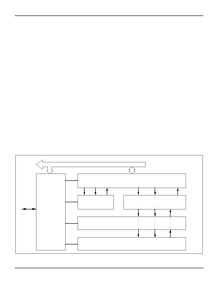
Figure 6 shows a typical system implementation.
Transparent latches are used to de-multiplex the R3081
address and data busses from the A/D bus. The data paths
between the memory system elements and the A/D bus is
managed by simple octal devices. A small set of simple PALs
is used to control the various data path elements, and to
control the handshake between the memory devices and the
CPU.
Depending on the cost vs. performance tradeoffs appropriate
to a given application, the system design engineer could
include true burst support from the DRAM to provide for high-
performance cache miss processing, or utilize a simpler,
lower performance memory system to reduce cost and simplify
the design. Similarly, the system designer could choose to
implement techniques such as external secondary cache, or
DMA, to further improve system performance.
DEVELOPMENT SUPPORT
The IDT R3051 family is supported by a rich set of
development tools, ranging from system simulation tools
through PROM monitor and debug support, applications
software and utility libraries, logic analysis tools, sub-system
modules, and shrink wrap operating systems. The R3081,
which is pin and software compatible with the R3051, can
directly utilize these existing tools to reduce time to market.
Figure 7 is an overview of the system development process
typically used when developing R3051 family applications.
The R3051 family is supported in all phases of project
development. These tools allow timely, parallel development
of hardware and software for R3051 family applications, and
include tools such as:
∑
Optimizing compilers from MIPS, the acknowledged leader
in optimizing compiler technology.
∑
Cross development tools, available in a variety of
development environments.
∑
The IDT Evaluation Board, which includes RAM, EPROM,
I/O, and the IDT PROM Monitor.
∑
IDT/sim
TM
, which implements a full prom monitor
(diagnostics, remote debug support, peek/poke, etc.).
∑
IDT/kit
TM
, which implements a run-time support package for
R3051 family systems.
PERFORMANCE OVERVIEW
The R3081 achieves a very high-level of performance. This
performance is based on:
∑
An efficient execution engine. The CPU performs ALU
operations and store operations in a single cycle, and has
an effective load time of 1.3 cycles, and branch execution
rate of 1.5 cycles (based on the ability of the compilers to
avoid software interlocks). Thus, the execution engine
achieves over 35 VUPS performance when operating out
of cache.
∑
A full featured floating point accelerator/co-processor.
The R3081 incorporates an R3010A compatible floating
point accelerator on-chip, with independent ALUs for floating
point add, multiply, and divide. The floating point unit is fully
hardware interlocked, and features overlapped operation
and precise exceptions. The FPA allows floating point
adds, multiplies, and divides to occur concurrently with
each other, as well as concurrently with integer operations.
∑
Large on-chip caches. The R3051 family contains caches
which are substantially larger than those on the majority of
today's microprocessors. These large caches minimize the
number of bus transactions required, and allow the R3051
family to achieve actual sustained performance very close
to its peak execution rate. The R3081 doubles the cache
available on the R3052, making it a suitable engine for

5.5
6
IDT79R3081 RISController
MILITARY AND COMMERCIAL TEMPERATURE RANGES
Figure 6. R3081 RISChipset Based System
ClkIn
IDT R3081
RISController
Address/Data
Control
I/O Controller
DRAM
Controller
DRAM
DRAM
PROM
I/O
I/O
IDT73720
Bus Exchanger
R3051
Local Bus
2889 drw 06
Figure 7. R3051 Family Development Toolchain
Cache-3051
SPP
Benchmarks
Evaluation Board
Laser Printer System
X-Terminal System
DBG Debugger
PIXIE Profiler
MIPS Compiler Suite
Stand-Alone Libraries
Floating Point Library
Cross Development Tools
Adobe PostScript PDL
MicroSoft TrueImage PDL
PeerlessPage Printer OS
X-Server
Hardware Models
General CAD Tools
Evaluation Board
Laser Printer System
Support Chips
Logic Analysis
Diagnostics
IDT/sim
IDT/kit
In-Circuit Emulation
Remote Debug
Real-Time OS
Software
Hardware
System
Integration
and Verfification
System
Development
Phase
System
Architecture
Evaluation
2889 drw 07

IDT79R3081 RISController
MILITARY AND COMMERICAL TEMPERATURE RANGES
5.5
7
many general purpose computing applications, such as ARC
compliant systems.
∑ Autonomous multiply and divide operations. The R3051
family features an on-chip integer multiplier/divide unit which is
separate from the other ALU. This allows the CPU to perform
multiply or divide operations in parallel with other integer oper-
ations, using a single multiply or divide instruction rather than
"step" operations.
∑ Integrated write buffer. The R3081 features a four deep
write buffer, which captures store target addresses and data at
the processor execution rate and retires it to main memory at
the slower main memory access rate. Use of on-chip write
buffers eliminates the need for the processor to stall when per-
forming store operations.
∑ Burst read support. The R3051 family enables the system
designer to utilize page mode or nibble mode RAMs when per-
forming read operations to minimize the main memory read
penalty and increase the effective cache hit rates.
These techniques combine to allow the processor to
achieve over 43 VUPS integer performance, 13MFlops of Lin-
pack performance, and 70,000 dhrystones without the use of
external caches or zero wait-state memory devices.
The performance differences between the various family
members depends on the application software and the design
of the memory system. The impact of the various cache sizes,
and the hardware floating point, can be accurately modeled
using Cache-3051. Since the R3041, R3051, R3052, R3071,
and R3081 are all pin and software compatible, the system
designer has maximum freedom in trading between perfor-
mance and cost. A system can be designed, and later the
appropriate CPU inserted into the board, depending on the
desired system performance.
SELECTABLE FEATURES
The R3081 allows the system designer to configure certain
aspects of operation. Some of these options are established
when the device is reset, while others are enabled via the
Config registers:
∑ BigEndian vs. LittleEndian Byte Ordering. The part can be
configured to operate with either byte ordering. ACE/ARC sys-
tems typically use Little Endian byte ordering. However, vari-
ous embedded applications, written originally for a Big Endian
processor such as the MC680x0, are easier to port to a Big
Endian system.
∑ Data Cache Refill of one or four words. The memory sys-
tem must be capable of performing four word refills of instruc-
tion cache misses. The R3081 allows the system designer to
enable D-Cache refill of one or four words dynamically. Thus,
specialized algorithms can choose one refill size, while the
rest of the system can operate with the other.
∑ Half-frequency bus mode. The processor can be config-
ured such that the external bus interface is at one-half the fre-
quency of the processor core. This simplifies system design;
however, the large on-chip caches mitigate the performance
impact of using a slower system bus clock.
∑ Slow bus turn-around. The R3081 allows the system
designer to space processor operations, so that more time
is allowed for transitions between memory and the processor
on the multiplexed address/data bus.
∑ Configurable cache. The R3081 allows the system designer
to use software to select either a 16kB Instruction Cache/4kB
Data Cache organization, or an 8kB Instruction/8kB Data
Cache organization.
∑ Cache Coherent Interface. The R3081 has an optional
hardware based cache coherency interface intended to sup-
port multi-master systems such as those utilizing DMA
between memory and I/O.
∑ Optional 1x or 2x clock input. The R3081 can be driven
with an R3051 compatible 2x clock input, or a lower frequency
1x clock input.
THERMAL CONSIDERATIONS
The R3081 utilizes special packaging techniques to
improve the thermal properties of high-speed processors.
Thus, the R3081 is packaged using cavity down packaging,
with an embedded thermal slug to improve thermal transfer to
the surrounding air.
The R3081 utilizes the 84-pin plastic package, with the die
being attached to a heat slug. The DL84 package allows for an
efficient thermal transfer between the die and the heat slug.
The heat slug offers a greater area for convection at any given
temperature. Even nominal amounts of airflow will dramatically
reduce the junction temperature of the die, resulting in cooler
operation. The DL84 package is available at all frequencies,
and is pin and form compatible with the PLCC used for the
R3051. Thus, designers can interchange R3081s and R3051s
in a particular design, without changing their PC Board.
The R3081 is guaranteed in a case temperature range of
0∞C to +85∞C. The type of package, speed (power) of the
device, and airflow conditions, affect the equivalent ambient
temperature conditions which will meet this specification.
The equivalent allowable ambient temperature, TA, can be
calculated using the thermal resistance from case to ambient
(ÿCA) of the given package. The following equation relates
ambient and case temperature:
TA = TC - P * ÿCA
where P is the maximum power consumption at hot tem-
perature, calculated by using the maximum Icc specification
for the device.
Typical values for ÿCA at various airflows are shown in
Table 1.
Note that the R3081 allows the operational frequency to be
turned down during idle periods to reduce power consumption.
This operation is described in the R3081 Hardware User's
Guide. Reducing the operation frequency dramatically
reduces power consumption.

IDT79R3081 RISController
MILITARY AND COMMERICAL TEMPERATURE RANGES
5.5
8
NOTES ON SYSTEM DESIGN
The R3081 has been designed to simplify the task of high-
speed system design. Thus, set-up and hold-time require-
ments have been kept to a minimum, allowing a wide variety of
system interface strategies.
To minimize these AC parameters, the R3081 employs
feedback from its SysClk output to the internal bus interface
unit. This allows the R3081 to reference input signals to the
reference clock seen by the external system. The SysClk out-
put is designed to provide relatively large AC drive to
minimize skew due to slow rise or fall times. A typical part will
have less than 2ns rise or fall (10% to 90% signal times) when
driving the test load.
Therefore, the system designer should use care when
designing for direct SysClk use. Total loading (due to devices
connected on the signal net and the routing of the net itself)
should be minimized to ensure the SysClk output has a
smooth and rapid transition. Long rise and/or fall times may
cause a degradation in the speed capability of an individual
device.
Similarly, the R3081 employs feedback on its ALE output to
ensure adequate address hold time to ALE. The system
designer should be careful when designing the ALE net to
minimize total loading and to minimize skew between ALE and
the A/D bus, which will ensure adequate address access latch
time.
IDT's field and factory applications groups can provide the
system designer with assistance for these and other design
issues.
Airflow (m/s)
0
1
2
3
4
5
DL84 ÿ
JA
21.0
12.8
12.0
9.9
9.2
8.5
DL84 ÿ
CA
18.3
10.1
9.3
7.2
6.6
5.8
PL84 ÿ
JA
36.6
29.6
27.0
26.2
25.4
24.8
PL84 ÿ
CA
18.3
10.1
9.3
7.2
6.6
5.8
Table 1 Thermal Resistance at Various Airflows
5.5
9
IDT79R3081 RISController
MILITARY AND COMMERCIAL TEMPERATURE RANGES
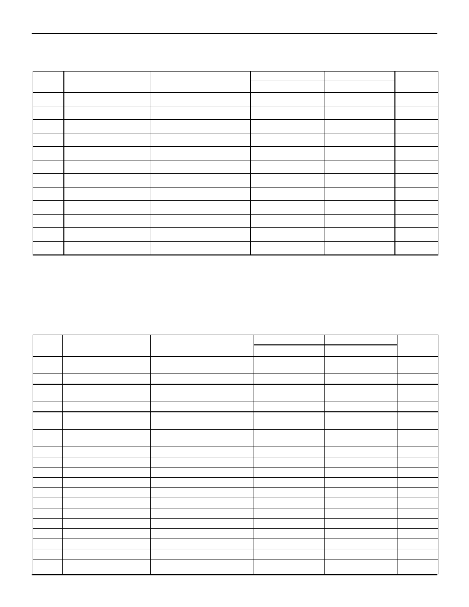
PIN DESCRIPTION
PIN NAME
I/O
DESCRIPTION
A/D(31:0)
I/O
Address/Data: A 32-bit time multiplexed bus which indicates the desired address for a bus transaction
in one phase, and which is used to transmit data between the CPU and external memory resources during
the rest of the transfer.
Bus transactions on this bus are logically separated into two phases: during the first phase, information
about the transfer is presented to the memory system to be captured using the ALE output. This
information consists of:
Address(31:4):
The high-order address for the transfer is presented on A/D(31:4).
BE
BE
(3:0):
These strobes indicate which bytes of the 32-bit bus will be involved in
the transfer, and are presented on A/D(3:0).
During write cycles, the bus contains the data to be stored and is driven from the internal write buffer.
On read cycles, the bus receives the data from the external resource, in either a single data transaction
or in a burst of four words, and places it into the on-chip read buffer.
During cache coherency operations, the R3081 monitors the A/D bus at the start of a DMA write to capture
the write target address for potential data cache invalidates.
Addr(3:2)
O
Low Address (3:2) A 2-bit bus which indicates which word is currently expected by the processor.
Specifically, this two bit bus presents either the address bits for the single word to be transferred (writes
or single datum reads) or functions as a two bit counter starting at `00' for burst read operations.
During cache coherency operations, the R3081 monitors the Addr bus at the start of a DMA write to
capture the write target address for potential data cache invalidates.
Diag(1)
O
Diagnostic Pin 1. This output indicates whether the current bus read transaction is due to an on-chip
cache miss, and also presents part of the miss address. The value output on this pin is time multiplexed:
Cached:
During the phase in which the A/D bus presents address information, this
pin is an active HIGH output which indicates whether the current read is
a result of a cache miss.
Miss Address (3):
During the remainder of the read operation, this output presents address
bit (3) of the address the processor was attempting to reference when the
cache miss occurred. Regardless of whether a cache miss is being
processed, this pin reports the transfer address during this time.
On write cycles, this output signals whether the data being written as retained in the on-chip data cache.
The value of this pin is time multiplexed during writes:
Cached:
During the address phase of write transactions, this signal is an active
high output which indicates that the store data was retained in the on-chip
data cache.
Reserved:
The value of this pin during the data phase of writes is reserved.
Diag(0)
O
Diagnostic Pin 0. This output distinguishes cache misses due to instruction references from those
due to data references, and presents the remaining bit of the miss address. The value output on this
pin is also time multiplexed:
I/
D
D
:
If the "Cached" Pin indicates a cache miss, then a high on this pin at this
time indicates an instruction reference, and a low indicates a data
reference. If the read is not due to a cache miss but rather an uncached
reference, then this pin is undefined during this phase.
Miss Address (2):
During the remainder of the read operation, this output presents
address bit (2) of the address the processor was attempting to
reference when the cache miss occurred. Regardless of whether a
cache miss is being processed, this pin reports the transfer address
during this time.
During write cycles, the value of this pin during both the address and data phases is reserved.
2889 tbl 02
5.5
10
IDT79R3081 RISController
MILITARY AND COMMERCIAL TEMPERATURE RANGES
PIN DESCRIPTION (Continued):
PIN NAME
I/O
DESCRIPTION
ALE
I/O
Address Latch Enable: Used to indicate that the A/D bus contains valid address information for the bus
transaction. This signal is used by external logic to capture the address for the transfer, typically using
transparent latches.
During cache coherency operations, the R3081 monitors ALE at the start of a DMA write, to capture the write
target address for potential data cache invalidates.
Rd
O
Read: An output which indicates that the current bus transaction is a read.
Wr
I/O
Write: An output which indicates that the current bus transaction is a write. During coherent DMA, this input
indicates that the current transfer is a write.
DataEn
O
External Data Enable: This signal indicates that the A/D bus is no longer being driven by the processor during
read cycles, and thus the external memory system may enable the drivers of the memory system onto this bus
without having a bus conflict occur. During write cycles, or when no bus transaction is occurring, this signal is
negated, thus disabling the external memory drivers
Burst/
O
Burst Transfer/Write Near: On read transactions, the
Burst
signal indicates that the current bus read is
WrNear
requesting a block of four contiguous words from memory. This signal is asserted only in read cycles due to
cache misses; it is asserted for all I-Cache miss read cycles, and for D-Cache miss read cycles if quad word refill
is currently selected.
On write transactions, the
WrNear
output tells the external memory system that the bus interface unit is
performing back-to-back write transactions to an address within the same 512 word page as the prior write
transaction. This signal is useful in memory systems which employ page mode or static column DRAMs, and
allows near writes to be retired quickly.
Ack
I
Acknowledge: An input which indicates to the device that the memory system has sufficiently processed the
bus transaction, and that the CPU may either terminate the write cycle or process the read data from this read
transfer.
During Coherent DMA, this input indicates that the current write transfer is completed, and that the internal
invalidation address counter should be incremented.
RdCEn
I
Read Buffer Clock Enable: An input which indicates to the device that the memory system has placed valid
data on the A/D bus, and that the processor may move the data into the on-chip Read Buffer.
SysClk
O
System Reference Clock: An output from the CPU which reflects the timing of the internal processor "Sys"
clock. This clock is used to control state transitions in the read buffer, write buffer, memory controller, and bus
interface unit. This clock will either be at the same frequency as the CPU execution rate clock, or at one-half
that frequency, as selected during reset.
BusReq
I
DMA Arbiter Bus Request: An input to the device which requests that the CPU tri-state its bus interface signals
so that they may be driven by an external master.
BusGnt
O
DMA Arbiter Bus Grant. An output from the CPU used to acknowledge that a
BusReq
has been detected, and
that the bus is relinquished to the external master.
IvdReq
I
Invalidate Request. An input provided by an external DMA controller to request that the CPU invalidate the
Data Cache line corresponding to the current DMA write target address. This signal is the same pin as Diag(0)
CohReq
I
Coherent DMA Request. An input used by the external DMA controller to indicate that the requested DMA
operations could involve hardware cache coherency. This signal is the Rsvd(0) of the R3051.
SBrCond(3:2)
I
Branch Condition Port: These external signals are internally connected to the CPU signals CpCond(3:0).
BrCond(0)
These signals can be used by the branch on co-processor condition instructions as input ports. There are two
types of Branch Condition inputs: the SBrCond inputs have special internal logic to synchronize the inputs, and
thus may be driven by asynchronous agents. The direct Branch Condition inputs must be driven synchronously.
Note that BrCond(1) is used by the internal FPA, and thus is not available on an external pin.
BusError
I
Bus Error: Input to the bus interface unit to terminate a bus transaction due to an external bus error. This signal
is only sampled during read and write operations. If the bus transaction is a read operation, then the CPU will
take a bus error exception.
2889 tbl 03
5.5
11
IDT79R3081 RISController
MILITARY AND COMMERCIAL TEMPERATURE RANGES
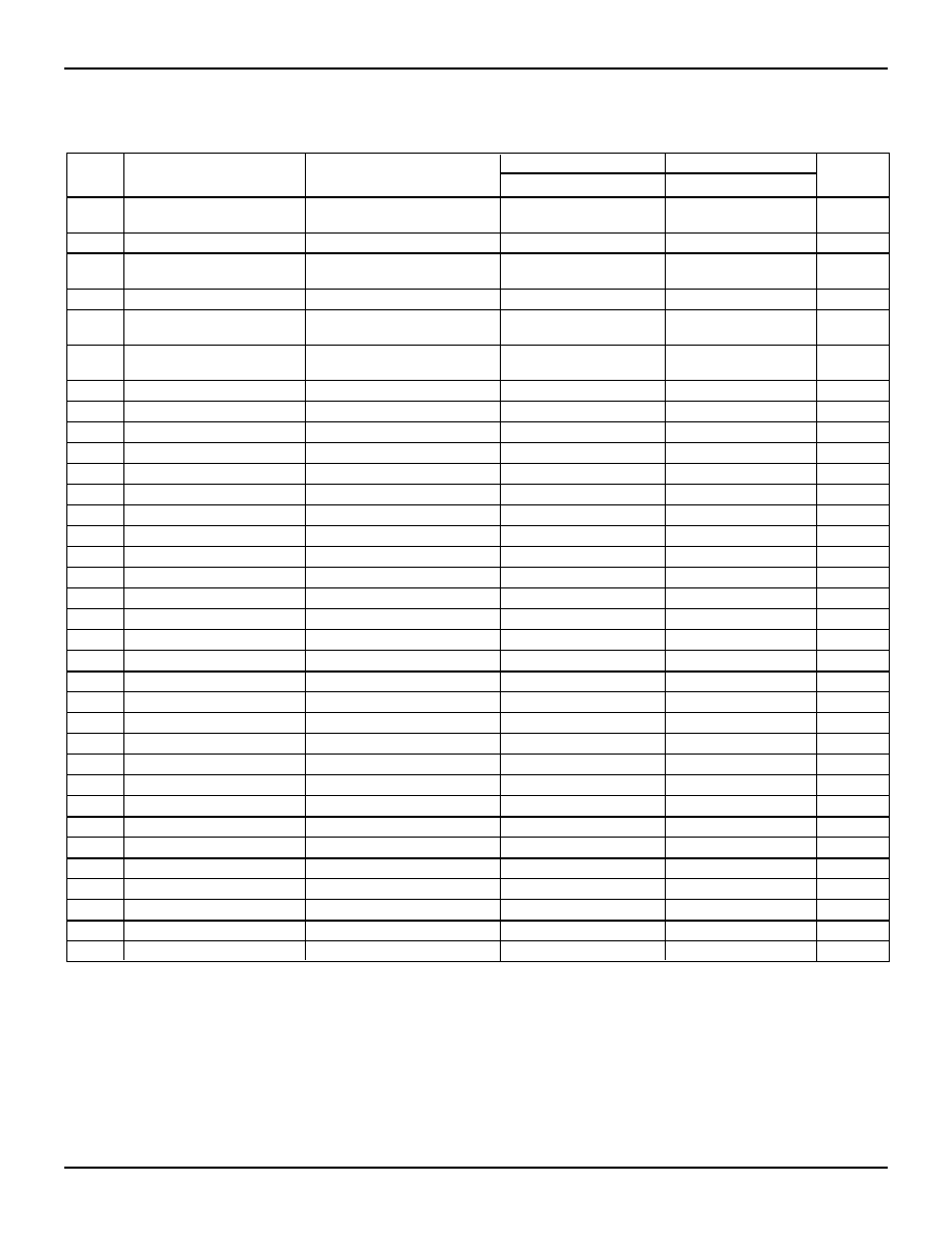
PIN NAME
I/O
DESCRIPTION
Int
(5:3)
I
Processor Interrupt: During normal operation, these signals are logically the same as the
Int
(5:0)
SInt
(2:0)
signals of the R3000. During processor reset, these signals perform mode initialization of the CPU, but in a
different (simpler) fashion than the interrupt signals of the R3000.
There are two types of interrupt inputs: the
SInt
inputs are internally synchronized by the processor, and may
be driven by an asynchronous external agent. The direct interrupt inputs are not internally synchronized, and
thus must be externally synchronized to the CPU. The direct interrupt inputs have one cycle lower latency than
the synchronized interrupts. Note that the interrupt used by the on-chip FPA will not be monitored externally.
ClkIn
I
Master Clock Input: This input clock can be provided at the execution frequency of the CPU (1x clock mode)
or at twice that frequency (2x clock mode), as selected at reset.
Reset
I
Master Processor Reset: This signal initializes the CPU. Mode selection is performed during the last cycle
of
Reset
.
Rsvd(4:1)
I/O
Reserved: These four signal pins are reserved for testing and for future revisions of this device. Users must not
connect these pins. Note that Rsvd(0) of the R3051 is now used for the
CohReq
input pin.
PIN DESCRIPTION (Continued):
ABSOLUTE MAXIMUM RATINGS
(1, 3)
Symbol
Rating
Commercial
Military
Unit
V
TERM
Terminal Voltage
≠0.5 to +7.0
≠0.5 to +7.0
V
with Respect
to GND
T
C
Operating Case
0 to +85
≠55 to +125
∞
C
Temperature
T
BIAS
Case Temperature ≠55 to +125
≠65 to +135
∞
C
Under Bias
T
STG
Storage
≠55 to +125
≠65 to +155
∞
C
Temperature
V
IN
Input Voltage
≠0.5 to +7.0
≠0.5 to +7.0
V
NOTES:
1. Stresses greater than those listed under ABSOLUTE MAXIMUM RATINGS
may cause permanent damage to the device. This is a stress rating only
and functional operation of the device at these or any other conditions
above those indicated in the operational sections of this specification is not
implied. Exposure to absolute maximum rating conditions for extended
periods may affect reliability.
2. V
IN
minimum = ≠3.0V for pulse width less than 15ns.
V
IN
should not exceed V
CC
+0.5V.
3. Not more than one output should be shorted at a time. Duration of the short
should not exceed 30 seconds.
2889 tbl 05
OUTPUT LOADING FOR AC TESTING
Signal
C
LD
SysClk
50 pf
All Others
25 pf
2889 tbl 08
Symbol
Parameter
Min.
Max.
Unit
V
IH
Input HIGH Voltage
3.0
--
V
V
IL
Input LOW Voltage
--
0
V
V
IHS
Input HIGH Voltage
3.0
--
V
V
ILS
Input LOW Voltage
--
0
V
2889 tbl 06
AC TEST CONDITIONS--RV3081
≠
+
To Device
Under Test
C
LD
≠4mA
+4mA
V
REF
+1.5V
2889 drw 08
AC TEST CONDITIONS--R3081
2889 tbl 06
Symbol
Parameter
Min.
Max.
Unit
V
IH
Input HIGH Voltage
3.0
--
V
V
IL
Input LOW Voltage
--
0
V
V
IHS
Input HIGH Voltage
3.5
--
V
V
ILS
Input LOW Voltage
--
0
V
2889 tbl 04
RECOMMENDED OPERATING
TEMPERATURE AND SUPPLY VOLTAGE
2889 tbl 07
Grade
Temperature(Case)
GND
V
CC
Military
≠55
∞
C to +125
∞
C
0V
5.0
±
10%
Commercial
0
∞
C to +85
∞
C
0V
5.0
±
5%
Commercial
0
∞
C to +85
∞
C
0V
3.3
±
5%
5.5
12
IDT79R3081 RISController
MILITARY AND COMMERCIAL TEMPERATURE RANGES
20MHz
25MHz
Symbol
Parameter
Test Conditions
Min.
Max.
Min.
Max.
Units
V
OH
Output HIGH Voltage
V
CC
= Min., I
OH
= ≠4mA
2.4
--
2.4
--
V
V
OL
Output LOW Voltage
V
CC
= Min., I
OL
= 4mA
--
0.4
--
0.4
V
V
IH
Input HIGH Voltage
(3)
--
2.0
--
2.0
--
V
V
IL
Input LOW Voltage
(1)
--
--
0.8
--
0.8
V
V
IHS
Input HIGH Voltage
(2,3)
--
2.8
--
2.8
--
V
V
ILS
Input LOW Voltage
(1,2)
--
--
0.4
--
0.4
V
C
IN
Input Capacitance
(4,5)
--
--
10
--
10
pF
C
OUT
Output Capacitance
(4,5)
--
--
10
--
10
pF
I
CC
Operating Current
V
CC
= 3.3V, T
A
= 25
∞
C
--
375
--
425
mA
I
IH
Input HIGH Leakage
V
IH
= VCC
--
100
--
100
µ
A
I
IL
Input LOW Leakage
V
IL
= GND
≠100
--
≠100
--
µ
A
I
OZ
Output Tri-state Leakage
V
OH
= 2.4V, V
OL
= 0.5V
≠100
100
≠100
100
µ
A
DC ELECTRICAL CHARACTERISTICS RV3081
COMMERCIAL TEMPERATURE RANGE
(1, 2)
--
(T
C
= 0
∞
C to +85
∞
C, V
CC
= +3.3V
±
5%)
2889 tbl 09
NOTES:
1. V
IL
Min. = ≠3.0V for pulse width less than 15ns. V
IL
should not fall below -0.5V for larger periods.
2. V
IHS
and V
ILS
apply to CIkIn and
Reset
.
3. V
IH
should not be held above V
CC
+ 0.5V.
4. Guaranteed by design.
5. ALE is 12pF for SysClk values C
IN
and C
OUT
for all speeds.
AC ELECTRICAL CHARACTERISTICS RV3081
COMMERCIAL TEMPERATURE RANGE
(1, 2)
--
(T
C
= 0
∞
C to +85
∞
C, V
CC
= +3.3V
±
5%)
20MHz
25MHz
Symbol
Signals
Description
Min.
Max.
Min.
Max.
Unit
t1
BusReq
,
Ack
,
BusError
,
Set-up to
SysClk
rising
6
--
5
--
ns
RdCEn
,
CohReq
t1a
A/D
Set-up to
SysClk
falling
7
--
6
--
ns
t2
BusReq
,
Ack
,
BusError
,
Hold from
SysClk
rising
4
--
4
--
ns
RdCEn
,
CohReq
t2a
A/D
Hold from
SysClk
falling
2
--
2
--
ns
t3
A/D, Addr, Diag, ALE,
Wr
Tri-state from
SysClk
rising
--
10
--
10
ns
Burst
/
WrNear
,
Rd
,
DataEn
t4
A/D, Addr, Diag, ALE,
Wr
Driven from
SysClk
falling
--
10
--
10
ns
Burst
/
WrNear
,
Rd
,
DataEn
t5
BusGnt
Asserted from
SysClk
rising
--
8
--
7
ns
t6
BusGnt
Negated from
SysClk
falling
--
8
--
7
ns
t7
Wr
,
Rd
,
Burst
/
WrNear
, A/D
Valid from
SysClk
rising
--
5
--
5
ns
t8
ALE
Asserted from
SysClk
rising
--
4
--
4
ns
t9
ALE
Negated from
SysClk
falling
--
4
--
4
ns
t10
A/D
Hold from ALE negated
(3)
2
--
2
--
ns
t11
DataEn
Asserted from
SysClk
falling
--
15
--
15
ns
t12
DataEn
Asserted from A/D tri-state
(3)
0
--
0
--
ns
t14
A/D
Driven from
SysClk
rising
(3)
0
--
0
--
ns
t15
Wr
,
Rd
,
DataEn
,
Burst
/
WrNear
Negated from
SysClk
falling
--
7
--
6
ns
t16
Addr(3:2)
Valid from
SysClk
--
6
--
6
ns
t17
Diag
Valid from
SysClk
--
12
--
11
ns
5.5
13
IDT79R3081 RISController
MILITARY AND COMMERCIAL TEMPERATURE RANGES
AC ELECTRICAL CHARACTERISTICS
RV3081 (cont.)
COMMERCIAL TEMPERATURE RANGE
(1, 2)
--
(T
C
= 0
∞
C to +85
∞
C, V
CC
= +3.3V
±
5%)
20MHz
25MHz
Symbol
Signals
Description
Min.
Max.
Min.
Max.
Unit
t18
A/D
Tri-state from
SysClk
falling
--
10
--
10
ns
t19
A/D
SysClk
falling to data valid
--
13
--
12
ns
t20
ClkIn (2x clock mode)
Pulse Width HIGH
10
--
8
--
ns
t21
ClkIn (2x clock mode)
Pulse Width LOW
10
--
8
--
ns
t22
ClkIn (2x clock mode)
Clock Period
25
250
20
250
ns
t23
Reset
Pulse Width from Vcc valid
200
--
200
--
µ
s
t24
Reset
Minimum Pulse Width
32
--
32
--
tsys
t25
Reset
Set-up to
SysClk
falling
6
--
5
--
ns
t26
Int
Mode set-up to
Reset
rising
10
--
9
--
ns
t27
Int
Mode hold from
Reset
rising
0
--
0
--
ns
t28
SInt
, SBrCond
Set-up to
SysClk
falling
6
--
5
--
ns
t29
SInt
, SBrCond
Hold from
SysClk
falling
3
--
3
--
ns
t30
Int
, BrCond
Set-up to
SysClk
falling
6
--
5
--
ns
t31
Int
, BrCond
Hold from
SysClk
falling
3
--
3
--
ns
tsys
SysClk
(full frequency mode)
Pulse Width
(5)
2*t22
2*t22
2*t22
2*t22
ns
t32
SysClk
(full frequency mode)
Clock High Time
(5)
t22-2
t22+2
t22-2
t22+2
ns
t33
SysClk
(full frequency mode)
Clock LOW Time
(5)
t22-2
t22+2
t22-2
t22+2
ns
tsys/2
SysClk
(half frequency mode)
Pulse Width
(5)
4*t22
4*t22
4*t22
4*t22
4*t22
ns
t34
SysClk
(half frequency mode)
Clock HIGH Time
(5)
2*t22-2
2*t22+2
2*t22-2
2*t22+2
ns
t35
SysClk
(half frequency mode)
Clock LOW Time
(5)
2*t22-2
2*t22+2
2*t22-2
2*t22+2
ns
t36
ALESet-up to
SysClk
falling
9
--
8
--
ns
t37
ALEHold from
SysClk
falling
2
--
2
--
ns
t38
A/DSet-up to ALE falling
10
--
9
--
ns
t39
A/DHold from ALE falling
2
--
2
--
ns
t40
Wr
Set-up to
SysClk
rising
10
--
9
--
ns
t41
Wr
Hold from
SysClk
rising
3
--
3
--
ns
t42
ClkIn (1x clock mode)
Pulse Width HIGH
(6)
20
--
16
--
ns
t43
ClkIn (1x clock mode)
Pulse Width LOW
(6)
20
--
16
--
ns
t44
ClkIn (1x clock mode)
Clock Period
(6)
50
50
40
50
ns
tderate
All outputs
Timing deration for loading
--
1
--
1
ns/
over C
LD
(3, 4)
25pF
NOTES:
2889 tbl 11
1. All timings referenced to 1.5V. All timings measured with respect to a 2.5ns rise and fall time.
2. The AC values listed here reference timing diagrams contained in the
R3081 Family Hardware User's Manual
.
3. Guaranteed by design.
4. This parameter is used to derate the AC timings according to the loading of the system. This parameter provides a deration for loads over the specified
test condition; that is, the deration factor is applied for each 25pF over the specified test load condition.
5. In 1x clock mode, t22 is replaced by t44/2.
6. In 1x clock mode, the design guarantees that the input clock rise and fall times can be as long as 5ns.
5.5
14
IDT79R3081 RISController
MILITARY AND COMMERCIAL TEMPERATURE RANGES
33MHz
40MHz
Symbol
Parameter
Test Conditions
Min.
Max.
Min.
Max.
Units
V
OH
Output HIGH Voltage
V
CC
= Min., I
OH
= ≠4mA
2.4
--
2.4
--
V
V
OL
Output LOW Voltage
V
CC
= Min., I
OL
= 4mA
--
0.4
--
0.4
V
V
IH
Input HIGH Voltage
(3)
--
2.0
--
2.0
--
V
V
IL
Input LOW Voltage
(1)
--
--
0.8
--
0.8
V
V
IHS
Input HIGH Voltage
(2,3)
--
2.8
--
2.8
--
V
V
ILS
Input LOW Voltage
(1,2)
--
--
0.4
--
0.4
V
C
IN
Input Capacitance
(4,5)
--
--
10
--
10
pF
C
OUT
Output Capacitance
(4,5)
--
--
10
--
10
pF
I
CC
Operating Current
V
CC
= 3.3V, T
A
= 25
∞
C
--
525
--
600
mA
I
IH
Input HIGH Leakage
V
IH
= VCC
--
100
--
100
µ
A
I
IL
Input LOW Leakage
V
IL
= GND
≠100
--
≠100
--
µ
A
I
OZ
Output Tri-state Leakage
V
OH
= 2.4V, V
OL
= 0.5V
≠100
100
≠100
100
µ
A
DC ELECTRICAL CHARACTERISTICS RV3081
COMMERCIAL TEMPERATURE RANGE
(1, 2)
--
(T
C
= 0
∞
C to +85
∞
C, V
CC
= +3.3V
±
5%)
2889 tbl 09
NOTES:
1. V
IL
Min. = ≠3.0V for pulse width less than 15ns. V
IL
should not fall below -0.5V for larger periods.
2. V
IHS
and V
ILS
apply to CIkIn and
Reset
.
3. V
IH
should not be held above V
CC
+ 0.5V.
4. Guaranteed by design.
5. ALE is 12pF for SysClk values C
IN
and C
OUT
for all speeds.
AC ELECTRICAL CHARACTERISTICS RV3081
COMMERCIAL TEMPERATURE RANGE
(1, 2)
--
(T
C
= 0
∞
C to +85
∞
C, V
CC
= +3.3V
±
5%)
33MHz
40MHz
Symbol
Signals
Description
Min.
Max.
Min.
Max.
Unit
t1
BusReq
,
Ack
,
BusError
,
Set-up to
SysClk
rising
4
--
3
--
ns
RdCEn
,
CohReq3
t1a
A/D
Set-up to
SysClk
falling
5
--
4.5
--
ns
t2
BusReq
,
Ack
,
BusError
,
Hold from
SysClk
rising
3
--
3
--
ns
RdCEn
,
CohReq
t2a
A/D
Hold from
SysClk
falling
1
--
1
--
ns
t3
A/D, Addr, Diag, ALE,
Wr
Tri-state from
SysClk
rising
--
10
--
10
ns
Burst
/
WrNear
,
Rd
,
DataEn
t4
A/D, Addr, Diag, ALE,
Wr
Driven from
SysClk
falling
--
10
--
10
ns
Burst
/
WrNear
,
Rd
,
DataEn
t5
BusGnt
Asserted from
SysClk
rising
--
6
--
5
ns
t6
BusGnt
Negated from
SysClk
falling
--
6
--
5
ns
t7
Wr
,
Rd
,
Burst
/
WrNear
, A/D
Valid from
SysClk
rising
--
4
--
3.5
ns
t8
ALE
Asserted from
SysClk
rising
--
3
--
3
ns
t9
ALE
Negated from
SysClk
falling
--
3
--
3
ns
t10
A/D
Hold from ALE negated
(3)
1.5
--
1.5
--
ns
t11
DataEn
Asserted from
SysClk
falling
--
13
--
12
ns
t12
DataEn
Asserted from A/D tri-state
(3)
0
--
0
--
ns
t14
A/D
Driven from
SysClk
rising
(3)
0
--
0
--
ns
t15
Wr
,
Rd
,
DataEn
,
Burst
/
WrNear
Negated from
SysClk
falling
--
5
--
4
ns
t16
Addr(3:2)
Valid from
SysClk
--
5
--
4.5
ns
t17
Diag
Valid from
SysClk
--
10
--
9
ns
5.5
15
IDT79R3081 RISController
MILITARY AND COMMERCIAL TEMPERATURE RANGES
AC ELECTRICAL CHARACTERISTICS
RV3081 (cont.)
COMMERCIAL TEMPERATURE RANGE
(1, 2)
--
(T
C
= 0
∞
C to +85
∞
C, V
CC
= +3.3V
±
5%)
33MHz
40MHz
Symbol
Signals
Description
Min.
Max.
Min.
Max.
Unit
t18
A/D
Tri-state from
SysClk
falling
--
9
--
8
ns
t19
A/D
SysClk
falling to data valid
--
11
--
10
ns
t20
ClkIn (2x clock mode)
Pulse Width HIGH
6.5
--
5.6
--
ns
t21
ClkIn (2x clock mode)
Pulse Width LOW
6.5
--
5.6
--
ns
t22
ClkIn (2x clock mode)
Clock Period
15
250
12.5
250
ns
t23
Reset
Pulse Width from Vcc valid
200
--
200
--
µ
s
t24
Reset
Minimum Pulse Width
32
--
32
--
tsys
t25
Reset
Set-up to
SysClk
falling
4
--
3
--
ns
t26
Int
Mode set-up to
Reset
rising
8
--
7
--
ns
t27
Int
Mode hold from
Reset
rising
0
--
0
--
ns
t28
SInt
, SBrCond
Set-up to
SysClk
falling
4
--
3
--
ns
t29
SInt
, SBrCond
Hold from
SysClk
falling
2
--
2
--
ns
t30
Int
, BrCond
Set-up to
SysClk
falling
4
--
3
--
ns
t31
Int
, BrCond
Hold from
SysClk
falling
2
--
2
--
ns
tsys
SysClk
(full frequency mode)
Pulse Width
(5)
2*t22
2*t22
2*t22
2*t22
ns
t32
SysClk
(full frequency mode)
Clock High Time
(5)
t22-1
t22+1
t22-1
t22+1
ns
t33
SysClk
(full frequency mode)
Clock LOW Time
(5)
t22-1
t22+1
t22-1
t22+1
ns
tsys/2
SysClk
(half frequency mode)
Pulse Width
(5)
4*t22
4*t22
4*t22
4*t22
4*t22
ns
t34
SysClk
(half frequency mode)
Clock HIGH Time
(5)
2*t22-1
2*t22+1
2*t22-1
2*t22+1
ns
t35
SysClk
(half frequency mode)
Clock LOW Time
(5)
2*t22-1
2*t22+1
2*t22-1
2*t22+1
ns
t36
ALESet-up to
SysClk
falling
7
--
6
--
ns
t37
ALEHold from
SysClk
falling
1
--
1
--
ns
t38
A/DSet-up to ALE falling
8
--
8
--
ns
t39
A/DHold from ALE falling
1
--
1
--
ns
t40
Wr
Set-up to
SysClk
rising
8
--
7
--
ns
t41
Wr
Hold from
SysClk
rising
3
--
3
--
ns
t42
ClkIn (1x clock mode)
Pulse Width HIGH
(6)
13
--
11
(6)
--
ns
t43
ClkIn (1x clock mode)
Pulse Width LOW
(6)
13
--
11
(6)
--
ns
t44
ClkIn (1x clock mode)
Clock Period
(6)
30
50
25
50
ns
tderate
All outputs
Timing deration for loading
--
1
--
1
ns/
over C
LD
(3, 4)
25pF
NOTES:
2889 tbl 11
1. All timings referenced to 1.5V. All timings measured with respect to a 2.5ns rise and fall time.
2. The AC values listed here reference timing diagrams contained in the
R3081 Family Hardware User's Manual
.
3. Guaranteed by design.
4. This parameter is used to derate the AC timings according to the loading of the system. This parameter provides a deration for loads over the specified
test condition; that is, the deration factor is applied for each 25pF over the specified test load condition.
5. In 1x clock mode, t22 is replaced by t44/2.
6. In 1x clock mode, the design guarantees that the input clock rise and fall times can be as long as 5ns .

5.5
16
IDT79R3081 RISController
MILITARY AND COMMERCIAL TEMPERATURE RANGES
20MHz
25MHz
33.33MHz
40MHz
50MHZ
Symbol
Parameter
Test Conditions
Min.
Max. Min. Max.
Min. Max.
Min. Max.
Min. Max. Units
V
OH
Output HIGH Voltage
V
CC
= Min., I
OH
= ≠4mA
3.5
--
3.5
--
3.5
--
3.5
--
3.5
--
V
V
OL
Output LOW Voltage
V
CC
= Min., I
OL
= 4mA
--
0.4
--
0.4
--
0.4
--
0.4
--
0.4
V
V
IH
Input HIGH Voltage
(3)
--
2.0
--
2.0
--
2.0
--
2.0
--
2.0
--
V
V
IL
Input LOW Voltage
(1)
--
--
0.8
--
0.8
--
0.8
--
0.8
--
0.8
V
V
IHS
Input HIGH Voltage
(2,3)
--
3.0
--
3.0
--
3.0
--
3.0
--
3.0
--
V
V
ILS
Input LOW Voltage
(1,2)
--
--
0.4
--
0.4
--
0.4
--
0.4
--
0.4
V
C
IN
Input Capacitance
(4)
--
--
10
--
10
--
10
--
10
--
10
pF
C
OUT
Output Capacitance
(4)
--
--
10
--
10
--
10
--
10
--
10
pF
I
CC
Operating Current
V
CC
= 5V, T
A
= 25
∞
C
--
475
--
525
--
625
--
700
--
825
mA
I
IH
Input HIGH Leakage
V
IH
= V
CC
--
100
--
100
--
100
--
100
--
100
µ
A
I
IL
Input LOW Leakage
V
IL
= GND
≠100
--
≠100
--
≠100
--
≠100
--
≠100
--
µ
A
I
OZ
Output Tri-state Leakage V
OH
= 2.4V, V
OL
= 0.5V ≠100
100 ≠100
100
≠100
100
≠100
100
≠100 100
µ
A
DC ELECTRICAL CHARACTERISTICS R3081
COMMERCIAL TEMPERATURE RANGE --
(T
C
= 0
∞
C to +85
∞
C, V
CC
= +5.0V
±
5%)
2889 tbl 09
NOTES:
1. V
IL
Min. = ≠3.0V for pulse width less than 15ns. V
IL
should not fall below -0.5V for larger periods.
2. V
IHS
and V
ILS
apply to CIkIn and
Reset
.
3. V
IH
should not be held above V
CC
+ 0.5V.
4. Guaranteed by design.
5.5
17
IDT79R3081 RISController
MILITARY AND COMMERCIAL TEMPERATURE RANGES
20MHz
25MHz
Symbol
Signals
Description
Min.
Max.
Min.
Max.
Unit
t1
BusReq
,
Ack
,
BusError
,
Set-up to
SysClk
rising
6
--
5
--
ns
RdCEn
,
CohReq
t1a
A/D
Set-up to
SysClk
falling
7
--
6
--
ns
t2
BusReq
,
Ack
,
BusError
,
Hold from
SysClk
rising
4
--
4
--
ns
RdCEn
,
CohReq
t2a
A/D
Hold from
SysClk
falling
2
--
2
--
ns
t3
A/D, Addr, Diag, ALE,
Wr
Tri-state from
SysClk
rising
--
10
--
10
ns
Burst
/
WrNear
,
Rd
,
DataEn
t4
A/D, Addr, Diag, ALE,
Wr
Driven from
SysClk
falling
--
10
--
10
ns
Burst
/
WrNear
,
Rd
,
DataEn
t5
BusGnt
Asserted from
SysClk
rising
--
8
--
7
ns
t6
BusGnt
Negated from
SysClk
falling
--
8
--
7
ns
t7
Wr
,
Rd
,
Burst
/
WrNear
, A/D
Valid from
SysClk
rising
--
5
--
5
ns
t8
ALE
Asserted from
SysClk
rising
--
4
--
4
ns
t9
ALE
Negated from
SysClk
falling
--
4
--
4
ns
t10
A/D
Hold from ALE negated
2
--
2
--
ns
t11
DataEn
Asserted from
SysClk
falling
--
15
--
15
ns
t12
DataEn
Asserted from A/D tri-state
(3)
0
--
0
--
ns
t14
A/D
Driven from
SysClk
rising
(3)
0
--
0
--
ns
t15
Wr
,
Rd
,
DataEn
,
Burst
/
WrNear
Negated from
SysClk
falling
--
7
--
6
ns
t16
Addr(3:2)
Valid from
SysClk
--
6
--
6
ns
t17
Diag
Valid from
SysClk
--
12
--
11
ns
t18
A/D
Tri-state from
SysClk
falling
--
10
--
10
ns
t19
A/D
SysClk
falling to data valid
--
13
--
12
ns
t20
ClkIn (2x clock mode)
Pulse Width HIGH
10
--
8
--
ns
t21
ClkIn (2x clock mode)
Pulse Width LOW
10
--
8
--
ns
t22
ClkIn (2x clock mode)
Clock Period
25
250
20
250
ns
t23
Reset
Pulse Width from V
CC
valid
200
--
200
--
µ
s
t24
Reset
Minimum Pulse Width
32
--
32
--
tsys
t25
Reset
Set-up to
SysClk
falling
6
--
5
--
ns
t26
Int
Mode set-up to
Reset
rising
10
--
9
--
ns
t27
Int
Mode hold from
Reset
rising
0
--
0
--
ns
t28
SInt
, SBrCond
Set-up to
SysClk
falling
6
--
5
--
ns
t29
SInt
, SBrCond
Hold from
SysClk
falling
3
--
3
--
ns
t30
Int
, BrCond
Set-up to
SysClk
falling
6
--
5
--
ns
t31
Int
, BrCond
Hold from
SysClk
falling
3
--
3
--
ns
tsys
SysClk
(full frequency mode)
Pulse Width
(5)
2*t22
2*t22
2*t22
2*t22
ns
t32
SysClk
(full frequency mode)
Clock HIGH Time
(5)
t22-2
t22+2
t22-2
t22+2
ns
AC ELECTRICAL CHARACTERISTICS R3081
COMMERCIAL TEMPERATURE RANGE
(1, 2)
(20, 25MHz)
--
(T
C
= 0
∞
C to +85
∞
C, V
CC
= +5.0V
±
5%)
2889 tbl 10
NOTES:
1. All timings referenced to 1.5V. All timings measured with respect to a 2.5ns rise and fall time.
2. The AC values listed here reference timing diagrams contained in the
R3081 Family Hardware User's Manual
.
3. Guaranteed by design.
4. This parameter is used to derate the AC timings according to the loading of the system. This parameter provides a deration for loads over the specified
test condition; that is, the deration factor is applied for each 25pF over the specified test load condition.
5. In 1x clock mode, t22 is replaced by t44/2.
6. In 1x clock mode, the design guarantees that the input clock rise and fall times can be as long as 5ns, 3ns for 40MHz and 50MHz.
7. When using the Reduced Frequency feature, the minimum allowed internal CPU speed is 0.5 MHz.

5.5
18
IDT79R3081 RISController
MILITARY AND COMMERCIAL TEMPERATURE RANGES
33MHz
40MHz
Symbol
Signals
Description
Min.
Max.
Min.
Max.
Unit
t1
BusReq
,
Ack
,
BusError
,
Set-up to
SysClk
rising
4
--
3
--
ns
RdCEn
,
CohReq
t1a
A/D
Set-up to
SysClk
falling
5
--
4.5
--
ns
t2
BusReq
,
Ack
,
BusError
,
Hold from
SysClk
rising
3
--
3
--
ns
RdCEn
,
CohReq
t2a
A/D
Hold from
SysClk
falling
1
--
1
--
ns
t3
A/D, Addr, Diag, ALE,
Wr
Tri-state from
SysClk
rising
--
10
--
10
ns
Burst
/
WrNear
,
Rd
,
DataEn
t4
A/D, Addr, Diag, ALE,
Wr
Driven from
SysClk
falling
--
10
--
10
ns
Burst
/
WrNear
,
Rd
,
DataEn
t5
BusGnt
Asserted from
SysClk
rising
--
6
--
5
ns
t6
BusGnt
Negated from
SysClk
falling
--
6
--
5
ns
t7
Wr
,
Rd
,
Burst
/
WrNear
, A/D
Valid from
SysClk
rising
--
4
--
3.5
ns
t8
ALE
Asserted from
SysClk
rising
--
3
--
3
ns
t9
ALE
Negated from
SysClk
falling
--
3
--
3
ns
t10
A/D
Hold from ALE negated
1.5
--
1.5
--
ns
t11
DataEn
Asserted from
SysClk
falling
--
13
--
12
ns
t12
DataEn
Asserted from A/D tri-state
(3)
0
--
0
--
ns
t14
A/D
Driven from
SysClk
rising
(3)
0
--
0
--
ns
t15
Wr
,
Rd
,
DataEn
,
Burst
/
WrNear
Negated from
SysClk
falling
--
5
--
4
ns
20MHz
25MHz
Symbol
Signals
Description
Min.
Max.
Min.
Max.
Unit
t33
SysClk
(full frequency mode)
Clock LOW Time
(5)
t22-2
t22+2
t22-2
t22+2
ns
tsys/2
SysClk
(half frequency mode)
Pulse Width
(5)
4*t22
4*t22
4*t22
4*t22
ns
t34
SysClk
(half frequency mode)
Clock HIGH Time
(5)
2*t22-2
2*t22+2
2*t22-2
2*t22+2
ns
t35
SysClk
(half frequency mode)
Clock LOW Time
(5)
2*t22-2
2*t22+2
2*t22-2
2*t22+2
ns
t36
ALE
Set-up to
SysClk
falling
9
--
8
--
ns
t37
ALE
Hold from
SysClk
falling
2
--
2
--
ns
t38
A/D
Set-up to ALE falling
10
--
9
--
ns
t39
A/D
Hold from ALE falling
2
--
2
--
ns
t40
Wr
Set-up to
SysClk
rising
10
--
9
--
ns
t41
Wr
Hold from
SysClk
rising
3
--
3
--
ns
t42
ClkIn (1x clock mode)
Pulse Width HIGH
(6)
20
--
16
--
ns
t43
ClkIn (1x clock mode)
Pulse Width LOW
(6)
20
--
16
--
ns
t44
ClkIn (1x clock mode)
Clock Period
(6)
50
50
40
50
ns
tderate
All outputs
Timing deration for loading
--
1
--
1
ns/
over C
LD
(3, 4)
25pF
AC ELECTRICAL CHARACTERISTICS
R3081 (cont.)
COMMERCIAL TEMPERATURE RANGE
(1, 2)
(20, 25MHz)
--
(T
C
= 0
∞
C to +85
∞
C, V
CC
= +5.0V
±
5%)
2889 tbl 11
NOTES:
1. All timings referenced to 1.5V. All timings measured with respect to a 2.5ns rise and fall time.
2. The AC values listed here reference timing diagrams contained in the
R3081 Family Hardware User's Manual
.
3. Guaranteed by design.
4. This parameter is used to derate the AC timings according to the loading of the system. This parameter provides a deration for loads over the specified
test condition; that is, the deration factor is applied for each 25pF over the specified test load condition.
5. In 1x clock mode, t22 is replaced by t44/2.
6. In 1x clock mode, the design guarantees that the input clock rise and fall times can be as long as 5ns, 3ns for 40MHz and 50MHz.
7. When using the Reduced Frequency feature, the minimum allowed internal CPU speed is 0.5 MHz.
AC ELECTRICAL CHARACTERISTICS R3081
COMMERCIAL TEMPERATURE RANGE
(1, 2)
(33, 40MHz)
--
(T
C
= 0
∞
C to +85
∞
C, V
CC
= +5.0V
±
5%)
2889 tbl 11
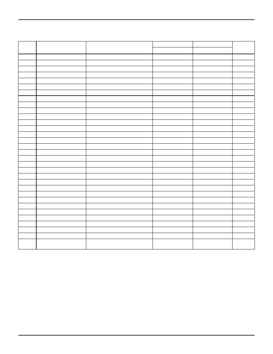
5.5
19
IDT79R3081 RISController
MILITARY AND COMMERCIAL TEMPERATURE RANGES
33MHz
40MHz
Symbol
Signals
Description
Min.
Max.
Min.
Max.
Unit
t16
Addr(3:2)
Valid from
SysClk
--
5
--
4.5
ns
t17
Diag
Valid from
SysClk
--
10
--
9
ns
t18
A/D
Tri-state from
SysClk
falling
--
9
--
8
ns
t19
A/D
SysClk
falling to data valid
--
11
--
10
ns
t20
ClkIn (2x clock mode)
Pulse Width HIGH
6.5
--
5.6
--
ns
t21
ClkIn (2x clock mode)
Pulse Width LOW
6.5
--
5.6
--
ns
t22
ClkIn (2x clock mode)
Clock Period
15
250
12.5
250
ns
t23
Reset
Pulse Width from V
CC
valid
200
--
200
--
µ
s
t24
Reset
Minimum Pulse Width
32
--
32
--
tsys
t25
Reset
Set-up to
SysClk
falling
4
--
3
ns
t26
Int
Mode set-up to
Reset
rising
8
--
7
--
ns
t27
Int
Mode hold from
Reset
rising
0
--
0
--
ns
t28
SInt
, SBrCond
Set-up to
SysClk
falling
4
--
3
--
ns
t29
SInt
, SBrCond
Hold from
SysClk
falling
2
--
2
--
ns
t30
Int
, BrCond
Set-up to
SysClk
falling
4
--
3
--
ns
t31
Int
, BrCond
Hold from
SysClk
falling
2
--
2
--
ns
tsys
SysClk
(full frequency mode)
Pulse Width
(5)
2*t22
2*t22
2*t22
2*t22
ns
t32
SysClk
(full frequency mode)
Clock HIGH Time
(5)
t22-1
t22+1
t22-1
t22+1
ns
t33
SysClk
(full frequency mode)
Clock LOW Time
(5)
t22-1
t22+1
t22-1
t22+1
ns
tsys/2
SysClk
(half frequency mode)
Pulse Width
(5)
4*t22
4*t22
4*t22
4*t22
ns
t34
SysClk
(half frequency mode)
Clock HIGH Time
(5)
2*t22-1
2*t22+1
2*t22-1
2*t22+1
ns
t35
SysClk
(half frequency mode)
Clock LOW Time
(5)
2*t22-1
2*t22+1
2*t22-1
2*t22+1
ns
t36
ALE
Set-up to
SysClk
falling
7
--
6
--
ns
t37
ALE
Hold from
SysClk
falling
1
--
1
--
ns
t38
A/D
Set-up to ALE falling
8
--
8
--
ns
t39
A/D
Hold from ALE falling
1
--
1
--
ns
t40
Wr
Set-up to
SysClk
rising
8
--
7
--
ns
t41
Wr
Hold from
SysClk
rising
3
--
3
--
ns
t42
ClkIn (1x clock mode)
Pulse Width HIGH
(6)
13
--
11
(6)
--
ns
t43
ClkIn (1x clock mode)
Pulse Width LOW
(6)
13
--
11
(6)
--
ns
t44
ClkIn (1x clock mode)
Clock Period
(6)
30
50
25
50
ns
tderate
All outputs
Timing deration for loading over C
LD
(3, 4)
--
1
--
1
ns/
25pF
AC ELECTRICAL CHARACTERISTICS R3081 (cont.)
COMERCIAL TEMPERATURE RANGE
(1, 2)
(33, 40MHz)
--
(T
C
= 0
∞
C to +85
∞
C, V
CC
= +5.0V
±
5%)
2889 tbl 11
NOTES:
1. All timings referenced to 1.5V. All timings measured with respect to a 2.5ns rise and fall time.
2. The AC values listed here reference timing diagrams contained in the
R3081 Family Hardware User's Manual
.
3. Guaranteed by design.
4. This parameter is used to derate the AC timings according to the loading of the system. This parameter provides a deration for loads over the specified
test condition; that is, the deration factor is applied for each 25pF over the specified test load condition.
5. In 1x clock mode, t22 is replaced by t44/2.
6. In 1x clock mode, the design guarantees that the input clock rise and fall times can be as long as 5ns, 3ns for 40 and 50MHz.
7. When using the Reduced Frequency feature, the minimum allowed internal CPU speed is 0.5 MHz.
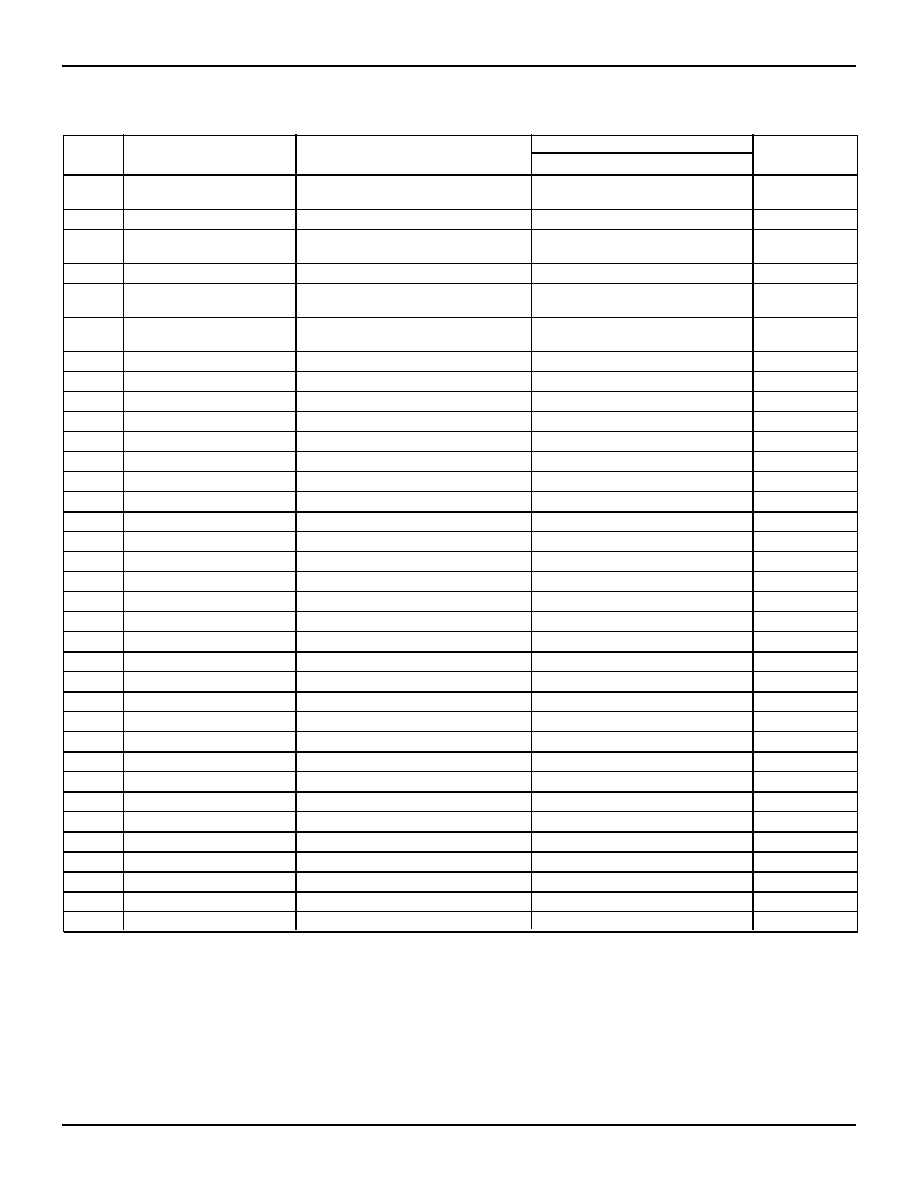
5.5
20
IDT79R3081 RISController
MILITARY AND COMMERCIAL TEMPERATURE RANGES
50MHz
Symbol
Signals
Description
Min.
Max.
Unit
t1
BusReq
,
Ack
,
BusError
,
Set-up to
SysClk
rising
5
--
ns
RdCEn
,
CohReq
t1a
A/D
Set-up to
SysClk
falling
6
--
ns
t2
BusReq
,
Ack
,
BusError
,
Hold from
SysClk
rising
4
--
ns
RdCEn
,
CohReq
t2a
A/D
Hold from
SysClk
falling
2
--
ns
t3
A/D, Addr, Diag, ALE,
Wr
Tri-state from
SysClk
rising
--
10
ns
Burst
/
WrNear
,
Rd
,
DataEn
t4
A/D, Addr, Diag, ALE,
Wr
Driven from
SysClk
falling
--
10
ns
Burst
/
WrNear
,
Rd
,
DataEn
t5
BusGnt
Asserted from
SysClk
rising
--
7
ns
t6
BusGnt
Negated from
SysClk
falling
--
7
ns
t7
Wr
,
Rd
,
Burst
/
WrNear
, A/D
Valid from
SysClk
rising
--
5
ns
t8
ALE
Asserted from
SysClk
rising
--
4
ns
t9
ALE
Negated from
SysClk
falling
--
4
ns
t10
A/D
Hold from ALE negated
1.5
--
ns
t11
DataEn
Asserted from
SysClk
falling
--
15
ns
t12
DataEn
Asserted from A/D tri-state
(3)
0
--
ns
t14
A/D
Driven from
SysClk
rising
(3)
0
--
ns
t15
Wr
,
Rd
,
DataEn
,
Burst
/
WrNear
Negated from
SysClk
falling
--
6
ns
t16
Addr(3:2)
Valid from
SysClk
--
6
ns
t17
Diag
Valid from
SysClk
--
11
ns
t18
A/D
Tri-state from
SysClk
falling
--
10
ns
t19
A/D
SysClk
falling to data valid
--
12
ns
t20
ClkIn (2x clock mode)
Pulse Width HIGH
N/A
(8)
ns
t21
ClkIn (2x clock mode)
Pulse Width LOW
N/A
(8)
ns
t22
ClkIn (2x clock mode)
Clock Period
N/A
(7, 8)
ns
t23
Reset
Pulse Width from V
CC
valid
200
--
µ
s
t24
Reset
Minimum Pulse Width
32
--
tsys
t25
Reset
Set-up to
SysClk
falling
5
ns
t26
Int
Mode set-up to
Reset
rising
9
--
ns
t27
Int
Mode hold from
Reset
rising
0
--
ns
t28
SInt
, SBrCond
Set-up to
SysClk
falling
5
--
ns
t29
SInt
, SBrCond
Hold from
SysClk
falling
3
--
ns
t30
Int
, BrCond
Set-up to
SysClk
falling
5
--
ns
t31
Int
, BrCond
Hold from
SysClk
falling
3
--
ns
tsys
SysClk
(full frequency mode)
Pulse Width
(5)
N/A
(8)
N/A
(8)
ns
t32
SysClk
(full frequency mode)
Clock HIGH Time
(5)
N/A
(8)
N/A
(8)
ns
t33
SysClk
(full frequency mode)
Clock LOW Time
(5)
N/A
(8)
N/A
(8)
ns
AC ELECTRICAL CHARACTERISTICS R3081
COMMERCIAL TEMPERATURE RANGE
(1, 2)
(50MHz)
--
(T
C
= 0
∞
C to +85
∞
C, V
CC
= +5.0V
±
5%)
NOTES:
1. All timings referenced to 1.5V. All timings measured with respect to a 2.5ns rise and fall time.
2. The AC values listed here reference timing diagrams contained in the
R3081 Family Hardware User's Manual
.
3. Guaranteed by design.
4. This parameter is used to derate the AC timings according to the loading of the system. This parameter provides a deration for loads over the specified
test condition; that is, the deration factor is applied for each 25pF over the specified test load condition.
5. In 1x clock mode, t22 is replaced by t44/2.
6. In 1x clock mode, the design guarantees that the input clock rise and fall times can be as long as 5ns, 3ns for 40MHz and 50MHz.
7. When using the Reduced Frequency feature, the minimum allowed internal CPU speed is 0.5 MHz.
8. For the 50MHz version, 1x Clock Mode and half-frequency bus mode only.
2889 tbl 11
5.5
21
IDT79R3081 RISController
MILITARY AND COMMERCIAL TEMPERATURE RANGES
AC ELECTRICAL CHARACTERISTICS R3081 (cont.)
COMERCIAL TEMPERATURE RANGE
(1, 2)
(50MHz)
--
(T
C
= 0
∞
C to +85
∞
C, V
CC
= +5.0V
±
5%)
50MHz
Symbol
Signals
Description
Min.
Max.
Unit
tsys/2
SysClk
(half frequency mode)
Pulse Width
(5)
2*t44
2*t44
ns
t34
SysClk
(half frequency mode)
Clock HIGH Time
(5)
t44-1
t44+1
ns
t35
SysClk
(half frequency mode)
Clock LOW Time
(5)
t44-1
t44+1
ns
t36
ALE
Set-up to
SysClk
falling
8
--
ns
t37
ALE
Hold from
SysClk
falling
2
--
ns
t38
A/D
Set-up to ALE falling
9
--
ns
t39
A/D
Hold from ALE falling
2
--
ns
t40
Wr
Set-up to
SysClk
rising
9
--
ns
t41
Wr
Hold from
SysClk
rising
3
--
ns
t42
ClkIn (1x clock mode)
Pulse Width HIGH
(6)
16
(6)
--
ns
t43
ClkIn (1x clock mode)
Pulse Width LOW
(6)
16
(6)
--
ns
t44
ClkIn (1x clock mode)
Clock Period
(6)
40
50
ns
tderate
All outputs
Timing deration for loading over C
LD
(3, 4)
--
1
ns/
25pF
NOTES:
1. All timings referenced to 1.5V. All timings measured with respect to a 2.5ns rise and fall time.
2. The AC values listed here reference timing diagrams contained in the
R3081 Family Hardware User's Manual
.
3. Guaranteed by design.
4. This parameter is used to derate the AC timings according to the loading of the system. This parameter provides a deration for loads over the specified
test condition; that is, the deration factor is applied for each 25pF over the specified test load condition.
5. In 1x clock mode, t22 is replaced by t44/2.
6. In 1x clock mode, the design guarantees that the input clock rise and fall times can be as long as 5ns, 3ns for 40MHz and 50MHz.
7. When using the Reduced Frequency feature, the minimum allowed internal CPU speed is 0.5 MHz.
8. For the 50MHz version, 1x Clock Mode and half-frequencybus mode only.

5.5
22
IDT79R3081 RISController
MILITARY AND COMMERCIAL TEMPERATURE RANGES
AC ELECTRICAL CHARACTERISTICS R3081
MILITARY TEMPERATURE RANGE
(1, 2)
--
(T
C
(7)
= -55
∞
C to +125
∞
C, V
CC
= +5.0V
±
10%)
20MHz
25MHz
Symbol
Signals
Description
Min.
Max.
Min.
Max.
Unit
t1
BusReq
,
Ack
,
BusError
,
Set-up to
SysClk
rising
6
--
5
--
ns
RdCEn
,
CohReq
t1a
A/D
Set-up to
SysClk
falling
7
--
6
--
ns
t2
BusReq
,
Ack
,
BusError
,
Hold from
SysClk
rising
4
--
4
--
ns
RdCEn
,
CohReq
t2a
A/D
Hold from
SysClk
falling
2
--
2
--
ns
t3
A/D, Addr, Diag, ALE,
Wr
Tri-state from
SysClk
rising
--
10
--
10
ns
Burst
/
WrNear
,
Rd
,
DataEn
t4
A/D, Addr, Diag, ALE,
Wr
Driven from
SysClk
falling
--
10
--
10
ns
Burst
/
WrNear
,
Rd
,
DataEn
t5
BusGnt
Asserted from
SysClk
rising
--
8
--
7
ns
t6
BusGnt
Negated from
SysClk
falling
--
8
--
7
ns
t7
Wr
,
Rd
,
Burst
/
WrNear
, A/D
Valid from
SysClk
rising
--
5
--
5
ns
t8
ALE
Asserted from
SysClk
rising
--
4.5
--
4.5
ns
t9
ALE
Negated from
SysClk
falling
--
4
--
4
ns
t10
A/D
Hold from ALE negated
(3)
1.5
--
1.5
--
ns
t11
DataEn
Asserted from
SysClk
falling
--
15
--
15
ns
t12
DataEn
Asserted from A/D tri-state
(3)
0
--
0
--
ns
t14
A/D
Driven from
SysClk
rising
(3)
0
--
0
--
ns
t15
Wr
,
Rd
,
DataEn
,
Burst
/
WrNear
Negated from
SysClk
falling
--
7
--
6
ns
t16
Addr(3:2)
Valid from
SysClk
--
6
--
6
ns
t17
Diag
Valid from
SysClk
--
12
--
11
ns
20MHz
25MHz
Symbol
Parameter
Test Conditions
Min.
Max.
Min.
Max.
Units
V
OH
Output HIGH Voltage
V
CC
= Min., I
OH
= ≠4mA
2.4
--
2.4
--
V
V
OL
Output LOW Voltage
V
CC
= Min., I
OL
= 4mA
--
0.4
--
0.4
V
V
IH
Input HIGH Voltage
(3)
--
2.0
--
2.0
--
V
V
IL
Input LOW Voltage
(1)
--
--
0.8
--
0.8
V
V
IHS
Input HIGH Voltage
(2,3)
--
2.8
--
2.8
--
V
V
ILS
Input LOW Voltage
(1,2)
--
--
0.4
--
0.4
V
C
IN
Input Capacitance
(4)
--
--
12
--
12
pF
C
OUT
Output Capacitance
(4)
--
--
12
--
12
pF
I
CC
Operating Current
V
CC
= 5.0V, T
A
= 25
∞
C
--
550
--
650
mA
I
IH
Input HIGH Leakage
V
IH
= VCC
--
100
--
100
µ
A
I
IL
Input LOW Leakage
V
IL
= GND
≠100
--
≠100
--
µ
A
I
OZ
Output Tri-state Leakage
V
OH
= 2.4V, V
OL
= 0.5V
≠100
100
≠100
100
µ
A
DC ELECTRICAL CHARACTERISTICS R3081
MILITARY TEMPERATURE RANGE--
(T
C
(5)
= -55
∞
C to +125
∞
C, V
CC
= +5.0V
±
10%)
2889 tbl 09
NOTES:
1. V
IL
Min. = ≠3.0V for pulse width less than 15ns. V
IL
should not fall below -0.5V for larger periods.
2. V
IHS
and V
ILS
apply to CIkIn and
Reset
.
3. V
IH
should not be held above V
CC
+ 0.5V.
4. Guaranteed by design.
5. Case Temperatures are "instant on."
5.5
23
IDT79R3081 RISController
MILITARY AND COMMERCIAL TEMPERATURE RANGES
AC ELECTRICAL CHARACTERISTICS
R3081 (cont.)
MILITARY TEMPERATURE RANGE
(1, 2)
--
(T
C
(7)
= -55
∞
C to +125
∞
C, V
CC
= +5.0V
±
10%)
20MHz
25MHz
Symbol
Signals
Description
Min.
Max.
Min.
Max.
Unit
t18
A/D
Tri-state from
SysClk
falling
--
10
--
10
ns
t19
A/D
SysClk
falling to data valid
--
13
--
12
ns
t20
ClkIn (2x clock mode)
Pulse Width HIGH
10
--
8
--
ns
t21
ClkIn (2x clock mode)
Pulse Width LOW
10
--
8
--
ns
t22
ClkIn (2x clock mode)
Clock Period
25
250
20
250
ns
t23
Reset
Pulse Width from Vcc valid
200
--
200
--
µ
s
t24
Reset
Minimum Pulse Width
32
--
32
--
tsys
t25
Reset
Set-up to
SysClk
falling
6
--
5
--
ns
t26
Int
Mode set-up to
Reset
rising
10
--
9
--
ns
t27
Int
Mode hold from
Reset
rising
0
--
0
--
ns
t28
SInt
, SBrCond
Set-up to
SysClk
falling
6
--
5
--
ns
t29
SInt
, SBrCond
Hold from
SysClk
falling
3.5
--
3
--
ns
t30
Int
, BrCond
Set-up to
SysClk
falling
6
--
5
--
ns
t31
Int
, BrCond
Hold from
SysClk
falling
3.5
--
3
--
ns
tsys
SysClk
(full frequency mode)
Pulse Width
(5)
2*t22
2*t22
2*t22
2*t22
ns
t32
SysClk
(full frequency mode)
Clock High Time
(5)
t22-2
t22+2
t22-2
t22+2
ns
t33
SysClk
(full frequency mode)
Clock LOW Time
(5)
t22-2
t22+2
t22-2
t22+2
ns
tsys/2
SysClk
(half frequency mode)
Pulse Width
(5)
4*t22
4*t22
4*t22
4*t22
ns
t34
SysClk
(half frequency mode)
Clock HIGH Time
(5)
2*t22-2
2*t22+2
2*t22-2
2*t22+2
ns
t35
SysClk
(half frequency mode)
Clock LOW Time
(5)
2*t22-2
2*t22+2
2*t22-2
2*t22+2
ns
t36
ALE
Set-up to
SysClk
falling
9
--
8
--
ns
t37
ALE
Hold from
SysClk
falling
2
--
2
--
ns
t38
A/D
Set-up to ALE falling
10
--
9
--
ns
t39
A/D
Hold from ALE falling
2
--
2
--
ns
t40
Wr
Set-up to
SysClk
rising
10
--
9
--
ns
t41
Wr
Hold from
SysClk
rising
3
--
3
--
ns
t42
ClkIn (1x clock mode)
Pulse Width HIGH
(6)
20
--
16
--
ns
t43
ClkIn (1x clock mode)
Pulse Width LOW
(6)
20
--
16
--
ns
t44
ClkIn (1x clock mode)
Clock Period
(6)
50
50
40
50
ns
tderate
All outputs
Timing deration for loading
--
1
--
1
ns/
over C
LD
(3, 4)
25pF
NOTES:
2889 tbl 11
1. All timings referenced to 1.5V. All timings measured with respect to a 2.5ns rise and fall time.
2. The AC values listed here reference timing diagrams contained in the
R3081 Family Hardware User's Manual
.
3. Guaranteed by design.
4. This parameter is used to derate the AC timings according to the loading of the system. This parameter provides a deration for loads over the specified
test condition; that is, the deration factor is applied for each 25pF over the specified test load condition.
5. In 1x clock mode, t22 is replaced by t44/2.
6. In 1x clock mode, the design guarantees that the input clock rise and fall times can be as long as 5ns.
7. Case Temperatures are "instant on."
5.5
24
IDT79R3081 RISController
MILITARY AND COMMERCIAL TEMPERATURE RANGES
PIN CONFIGURATIONS
NOTE:
Reserved Pins must not be connected.
Vss
Vcc
A/D(14)
A/D(13)
A/D(12)
A/D(11)
A/D(10)
A/D(9)
Vcc
Vss
A/D(8)
A/D(7)
A/D(6)
A/D(5)
A/D(4)
A/D(3)
Vss
Vcc
A/D(2)
A/D(1)
A/D(0)
Burst/WrNear
Addr(3)
Addr(2)
Vcc
Vss
Diag(1)
ALE
Rd
Wr
DataEn
Vcc
Vss
SysClk
BusGnt
Reset
BusError
Ack
RdCEn
BusReq
BrCond(0)
Vss
Vcc
ClkIn
Rsvd(4)
Rsvd(3)
Rsvd(2)
Rsvd(1)
CohReq
Int(5)
Vss
Vcc
Int(4)
Int(3)
SInt(2)
SInt(1)
SInt(0)
SBrCond(3)
SBrCond(2)
NC
Vss
Vcc
A/D(15)
A/D(16)
A/D(17)
A/D(18)
A/D(19)
A/D(20)
Vss
Vcc
A/D(21)
A/D(22)
A/D(23)
A/D(24)
A/D(25)
A/D(26)
Vcc
Vss
A/D(27)
A/D(28)
A/D(29)
A/D(30)
A/D(31)
1
84
12
75
33
54
Diag(0)/
IvdReq
2889 drw 08
84-Pin DL/PLCC
Top View
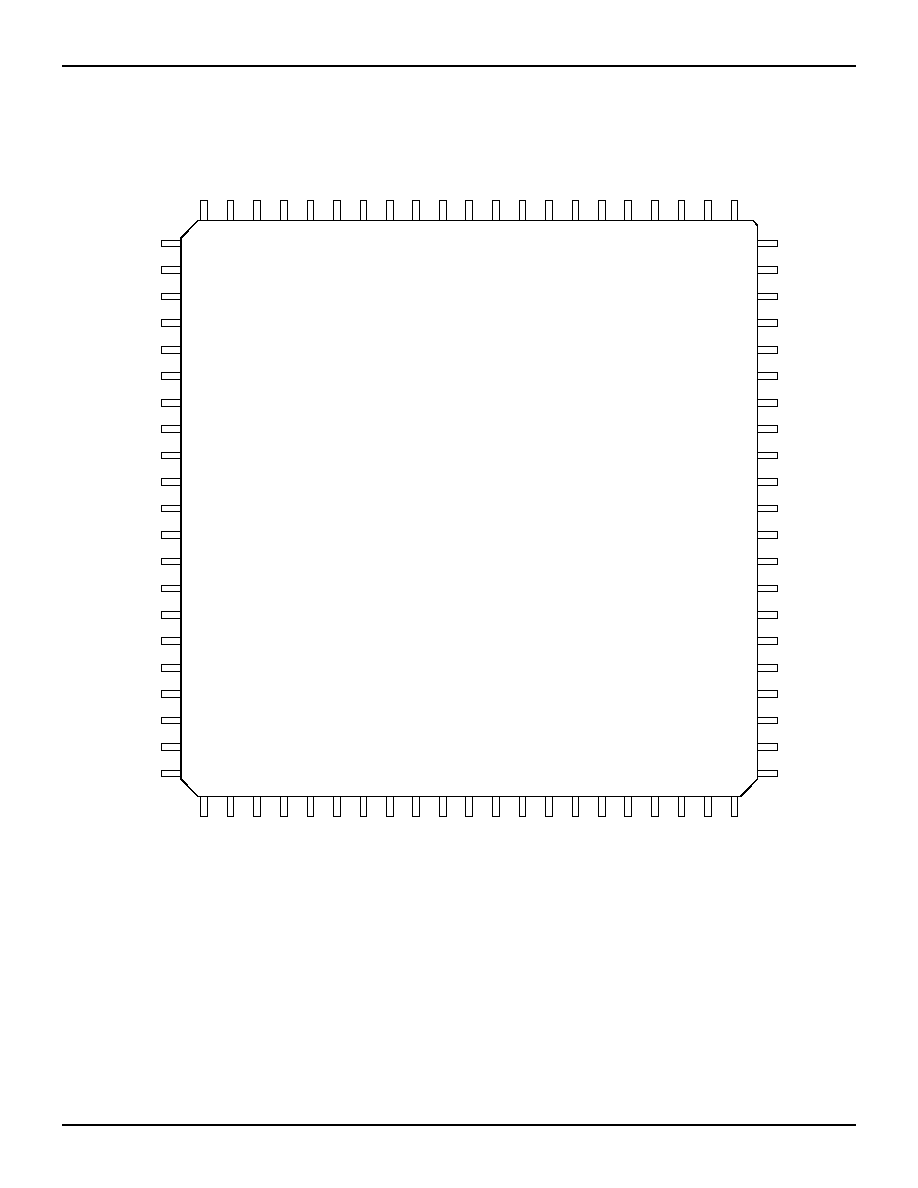
5.5
25
IDT79R3081 RISController
MILITARY AND COMMERCIAL TEMPERATURE RANGES
Vss
Vcc
A/D(14)
A/D(13)
A/D(12)
A/D(11)
A/D(10)
A/D(9)
Vcc
Vss
A/D(8)
A/D(7)
A/D(6)
A/D(5)
A/D(4)
A/D(3)
Vss
Vcc
A/D(2)
A/D(1)
A/D(0)
Burst/WrNear
Addr(3)
Addr(2)
Vcc
Vss
Diag(1)
ALE
Rd
Wr
DataEn
Vcc
Vss
SysClk
BusGnt
Reset
BusError
Ack
RdCEn
BusReq
BrCond(0)
Vss
Vcc
ClkIn
Rsvd(4)
Rsvd(3)
Rsvd(2)
Rsvd(1)
CohReq
Int(5)
Vss
Vcc
Int(4)
Int(3)
SInt(2)
SInt(1)
SInt(0)
SBrCond(3)
SBrCond(2)
NC
Vss
Vcc
A/D(15)
A/D(16)
A/D(17)
A/D(18)
A/D(19)
A/D(20)
Vss
Vcc
A/D(21)
A/D(22)
A/D(23)
A/D(24)
A/D(25)
A/D(26)
Vcc
Vss
A/D(27)
A/D(28)
A/D(29)
A/D(30)
A/D(31)
1
84
21
75
43
64
Diag(0)/
IvdReq
63
42
22
PIN CONFIGURATIONS
NOTE:
Reserved Pins must not be connected.
84-Pin FD
Top View
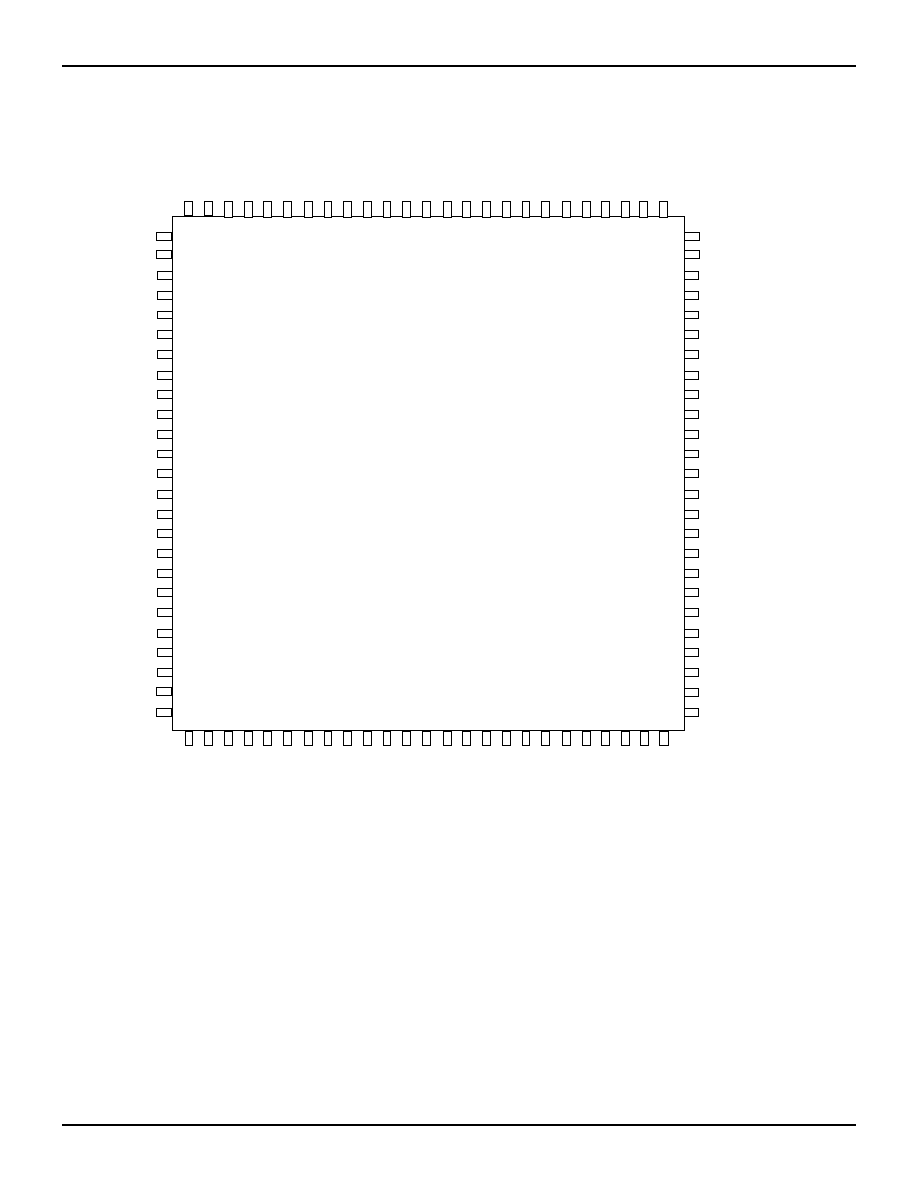
5.5
26
IDT79R3081 RISController
MILITARY AND COMMERCIAL TEMPERATURE RANGES
2905 drw 06
1
12
13
14
2
3
4
5
6
7
8
9
10
11
15
16
17
18
19
20
21
22
23
24
25
26
27
28
29
30
31
32
33
34
35
36
37
38
39
40
41
42
43
44
45
46
47
48
49
50
54
52 53
55 56 57 58 59 60
51
61 62 63 64 65 66 67 68 69 70 71 72 73 74 75
76
77
78
79
80
81
82
83
84
85
86
87
88
89
90
91
92
93
94
95
96
97
98
99
100
RV3081 Y
100-Pin
TQFP
(Cavity Up)
Top View
V
CC
A/D(14)
A/D(13)
A/D(12)
A/D(11)
A/D(10)
A/D(9)
V
CC
V
SS
A/D(8)
A/D(7)
A/D(6)
A/D(5)
A/D(4)
A/D(3)
V
SS
V
CC
A/D(2)
A/D(1)
A/D(0)
NC
NC
NC
NC
V
SS
SBrCond(2)
SBrCond(3)
V
CC
ClkIn
Int(5)
V
SS
V
CC
Int(4)
Int(3)
SInt(2)
SInt(1)
SInt(0)
V
SS
V
CC
NC
NC
NC
RSVD(4)
RSVD(3)
RSVD(2)
RSVD(1)
CohReQ
V
SS
V
SS
V
CC
Burst/WrNear
Addr(3)
Addr(2)
Diag(1)
ALE
Rd Wr
DataEn
V
CC
V
SS
SysClk
BusGnt
Reset
BusError
Ack
RdCEn
BusReq
V
CC
V
SS
BrCond(0)
DIAG0/
IvdReq
V
SS
V
CC
V
SS
V
CC
A/D(15)
A/D(16)
A/D(17)
A/D(18)
A/D(19)
A/D(20)
A/D(21)
A/D(22)
A/D(23)
A/D(24)
A/D(25)
A/D(26)
A/D(27)
A/D(28)
A/D(29)
A/D(30)
A/D(31)
V
CC
V
SS
V
CC
V
SS
NC
V
SS
V
SS
V
CC

5.5
27
IDT79R3081 RISController
MILITARY AND COMMERCIAL TEMPERATURE RANGES
Figure 8 (a). R3081 Clocking (1x clock input mode, full frequency bus)
Figure 8 (b). R3081Clocking (1x clock input mode, half-frequency bus)
Figure 8 (c). R3081 Clocking (2x clock input mode, half-frequency bus)
Figure 8 (d). R3081 Clocking (2x clock input mode, full-frequency bus)
ClkIn
SysClk
t
42
t
43
t
44
t
32
t
sys
t
33
2889 drw 12
ClkIn
SysClk
t
42
t
43
t
44
t
34
t
sys/2
t
35
2889 drw 13
ClkIn
SysClk
t
20
t
21
t
22
t
35
t
sys/2
t
34
2889 drw 14
ClkIn
SysClk
t
20
t
21
t
22
t
32
t
SYS
t
33
2889 drw 15
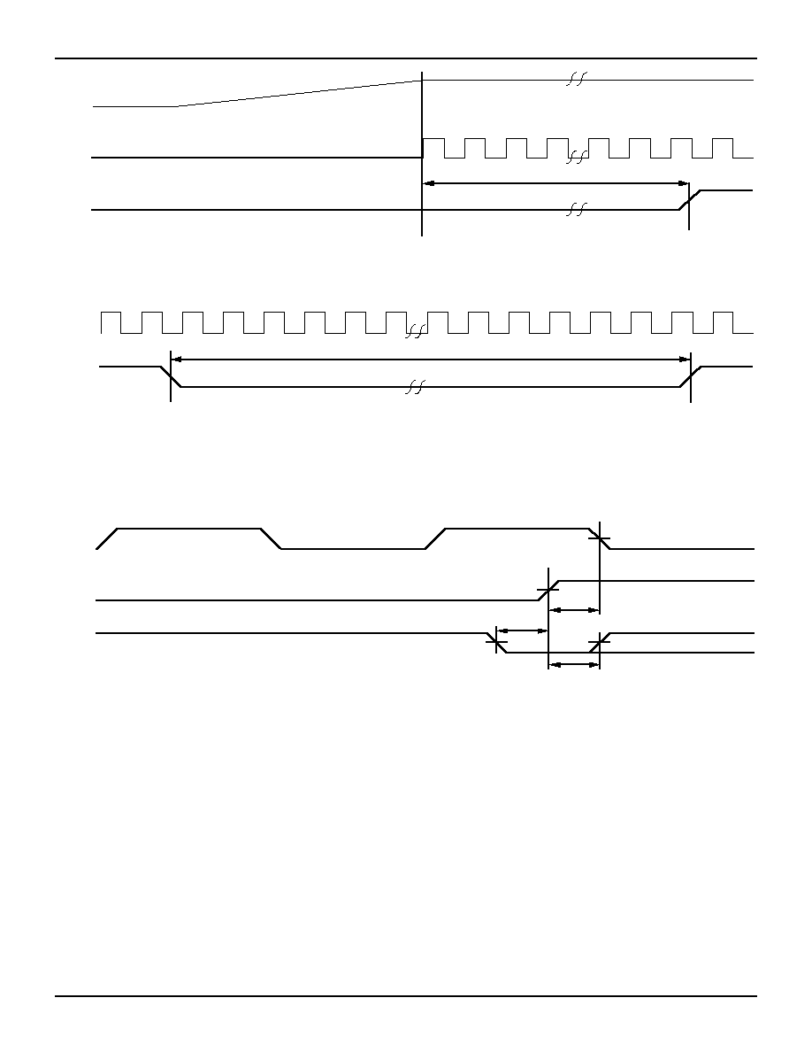
5.5
28
IDT79R3081 RISController
MILITARY AND COMMERCIAL TEMPERATURE RANGES
Figure 9. Power-On Reset Sequence
Figure 10. Warm Reset Sequence
Figure 11. Mode Selection and Negation of Reset
Vcc
ClkIn
Reset
t
23
2889 drw 16
ClkIn
Reset
t
24
2889 drw 17
SysClk
Reset
Int(n)
t
25
t
26
t
27
2889 drw 18
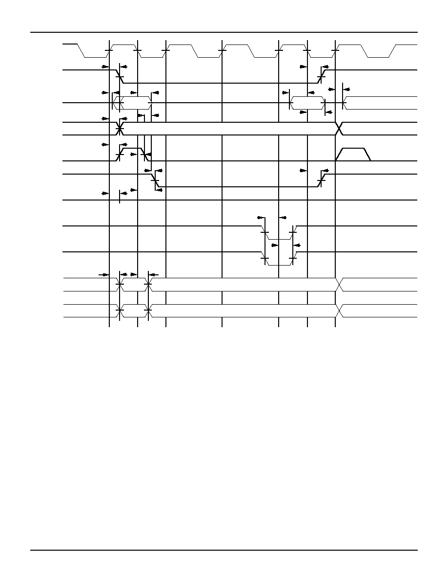
5.5
29
IDT79R3081 RISController
MILITARY AND COMMERCIAL TEMPERATURE RANGES
Figure 12. Single Datum Read in R3081
SysClk
Rd
A/D(31:0)
ALE
Addr(3:2)
DataEn
RdCEn
Ack
Burst
Diag(1)
Diag(0)
Addr
BE
Word Address
Start
Read
Turn
Bus
Ack?
Ack?
Sample
Data
End
Read
Ack/
RdCen
Cached?
I/D
Miss Address(2)
Miss Address(3)
Data Input
t
7
t
14
t
10
t
8
t
9
t
7
t
12
t
1
t
2
t
15
t
2a
t
15
t
1a
t
14
t
17
t
17
t
18
t
16
t
11
2889 drw 19
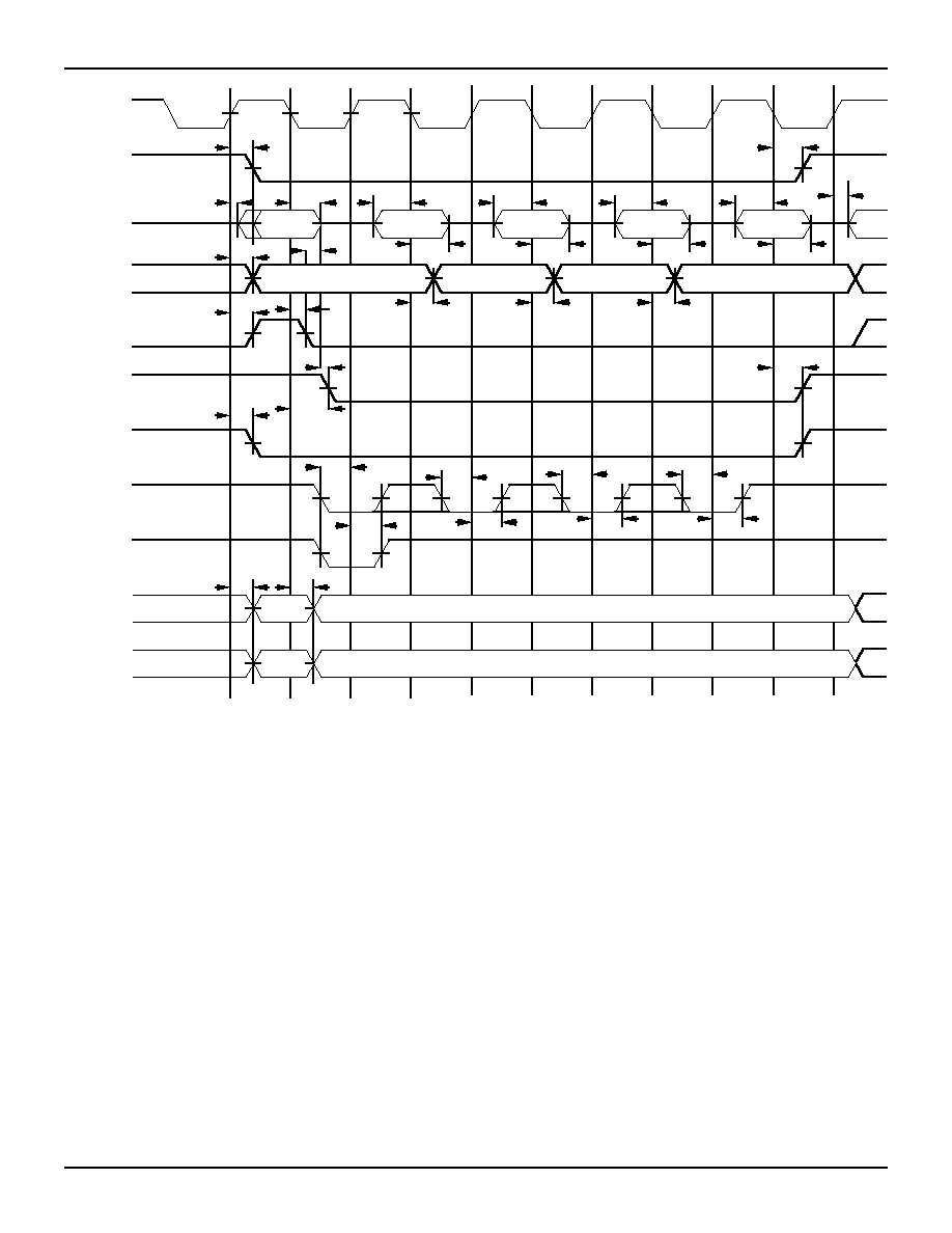
5.5
30
IDT79R3081 RISController
MILITARY AND COMMERCIAL TEMPERATURE RANGES
Figure 13. R3081 Burst Read
SysClk
Rd
A/D(31:0)
ALE
Addr(3:2)
DataEn
RdCEn
Ack
Burst
Diag(1)
Diag(0)
Addr
BE
'00'
Start
Read
Turn
Bus
Sample
Data
New
Transaction
Ack/
RdCen
Cached?
I/D
t
7
t
14
t
10
t
8
t
9
t
7
t
12
t
1
t
2
t
17
t
17
t
18
t
15
Word 0
t
2a
t
1a
t
14
t
15
Word 1
t
2a
t
1a
Word 2
t
2a
t
1a
Word 3
t
2a
t
1a
'01'
'10'
'11'
t
1
t
2
t
1
t
2
t
1
t
2
t
16
t
16
t
16
Sample
Data
Sample
Data
Sample
Data
RdCEn
RdCEn
RdCEn
Miss Address(2)
Miss Address(3)
t
16
t
11
2889 drw 20
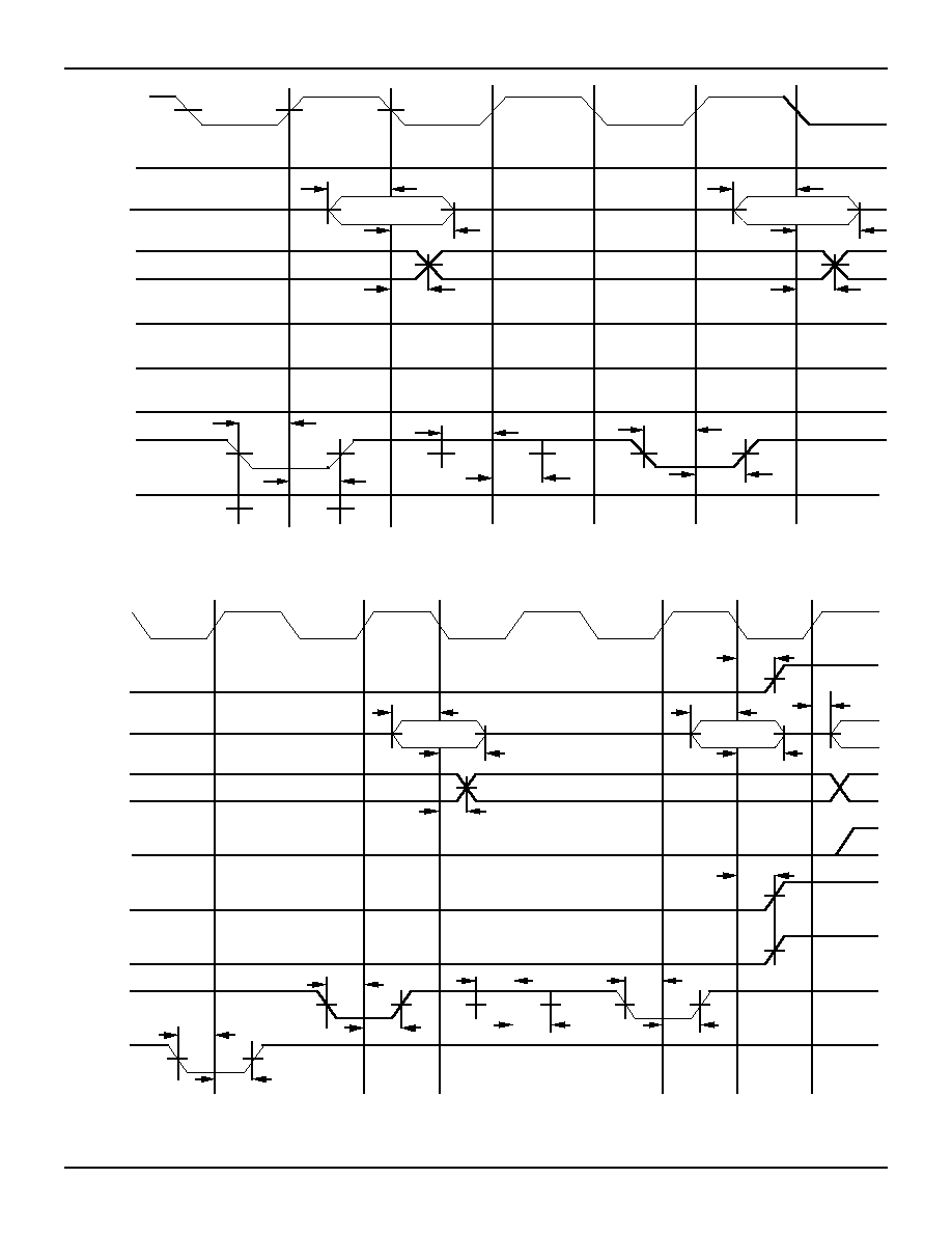
5.5
31
IDT79R3081 RISController
MILITARY AND COMMERCIAL TEMPERATURE RANGES
Figure 14 (b). End of Throttled Quad Read
Figure 14 (a). Start of Throttled Quad Read
SysClk
Rd
A/D(31:0)
ALE
Addr(3:2)
DataEn
RdCEn
Ack
Burst
'00'
Sample
Data
t
1
t
2
Word 0
t
2a
t
1a
Word 1
t
2a
t
1a
'01'
'10'
t
1
t
2
t
1
t
2
t
16
t
16
Sample
Data
Sample
Data
RdCEn
RdCEn
RdCEn
2889 drw 21
SysClk
Rd
A/D(31:0)
ALE
Addr(3:2)
DataEn
RdCEn
Ack
Burst
New
Transaction
Ack
t
15
t
14
t
15
t
2a
t
1a
Word 2
Word 3
t
2a
t
1a
'01'
'11'
t
1
t
2
t
1
t
2
t
1
t
2
t
16
Sample
Data
Sample
Data
RdCEn
RdCEn
t
1
t
2
2889 drw 22

5.5
32
IDT79R3081 RISController
MILITARY AND COMMERCIAL TEMPERATURE RANGES
Figure 16. Request and Relinquish of R3081 Bus to External Master
Figure 15. R3081 Write Cycle
SysClk
Wr
A/D(31:0)
ALE
Addr(3:2)
Ack
WrNear
Diag(1)
Diag(0)
Addr
BE
Word Address
Start
Write
Data
Out
Ack?
Ack?
Negate
Wr
New
Transfer
Ack
t
7
t
14
t
10
t
8
t
9
t
7
t
1
t
2
t
15
t
14
t
19
Data
Out
t
15
t
16
t
17
t
17
Reserved
Reserved
Reserved
Cached
2889 drw 23
A/D(31:0)
Addr(3:2)
Diag(1:0)
SysClk
BusReq
BusGnt
Rd
Wr
ALE
Burst/
WrNear
t
1
t
2
t
5
t
3
2889 drw 24
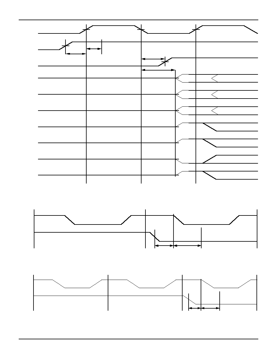
5.5
33
IDT79R3081 RISController
MILITARY AND COMMERCIAL TEMPERATURE RANGES
Figure 17. R3081 Regaining Bus Mastership
SysClk
BusReq
BusGnt
A/D(31:0)
Addr(3:2)
Diag(1:0)
Rd
Wr
ALE
Burst/
WrNear
t
1
t
2
t
6
t
4
2889 drw 25
Figure 18. Synchronized Interrupt Input Timing
Figure 19. Direct Interrupt Input Timing
SysClk
Int(n)
t
30
t
31
2889 drw 27
SysClk
SInt(n)
t
28
t
29
2889 drw 26
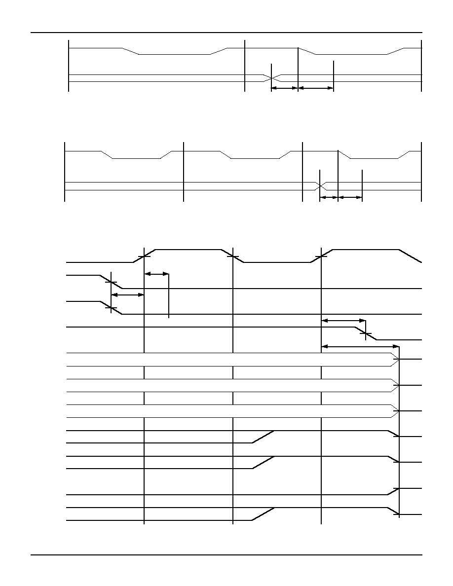
5.5
34
IDT79R3081 RISController
MILITARY AND COMMERCIAL TEMPERATURE RANGES
Figure 20. Synchronized Branch Condition Input Timing
SysClk
SBrCond(n)
t
28
t
29
2889 drw 28
Figure 22. Coherent DMA Request
SysClk
BusReq
BusGnt
A/D(31:0)
Addr(3:2)
Diag(1:0)
Rd
Wr
ALE
Burst/
WrNear
CohReq
t
1
t
2
t
5
t
3
2889 drw 30
Figure 21. Direct Branch Condition Input Timing
SysClk
BrCond(n)
t
30
t
31
2889 drw 29
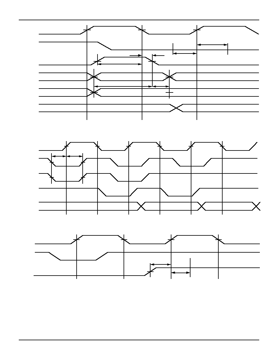
5.5
35
IDT79R3081 RISController
MILITARY AND COMMERCIAL TEMPERATURE RANGES
Figure 23. Beginning of Coherent DMA Write
SysClk
Wr
ALE
A/D
Addr
Internal
Invalidate
Address
T
36
T
37
T
40
T
41
T
38
T
39
2889 drw 31
Figure 24. Cache Word Invalidation
SysClk
Ack
IvdReq
Internal
Ivd
Internal
Invalidate
Address
T
1
T
2
2988 drw 32
Figure 25. End of Coherent Write
SysClk
Ack
Wr
T
40
T
41
2889 drw 33
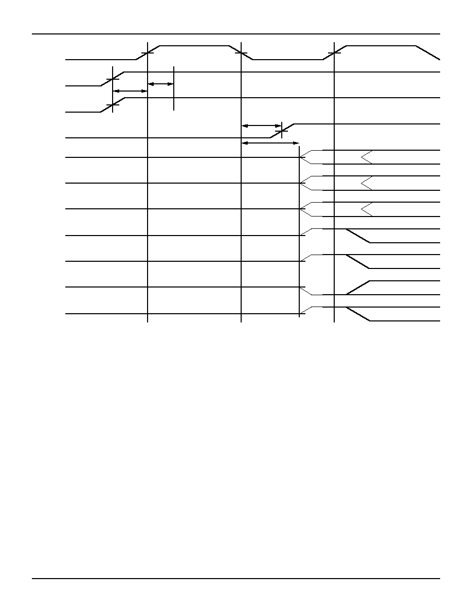
5.5
36
IDT79R3081 RISController
MILITARY AND COMMERCIAL TEMPERATURE RANGES
Figure 26. End of Coherent DMA Request
SysClk
BusReq
BusGnt
A/D(31:0)
Addr(3:2)
Diag(1:0)
Rd
Wr
ALE
Burst/
WrNear
CohReq
t
1
t
2
t
6
t
4
2889 drw 34
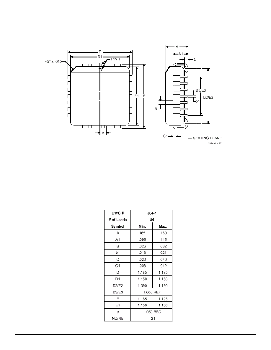
IDT79R3081 RISController
MILITARY AND COMMERICAL TEMPERATURE RANGES
5.5
37
84 LEAD PLCC/DL
(7)
(SQUARE)
NOTES:
1. All dimensions are in inches, unless otherwise noted.
2. BSC--Basic lead Spacing between Centers.
3. D & E do not include mold flash or protutions.
4. Formed leads shall be planar with respect to one another and within .004" at the seating plane.
5. ND & NE represent the number of leads in the D & E directions respectively.
6. D1 & E1 should be measured from the bottom of the package.
7. DL is pin & form compatible with PLCC.

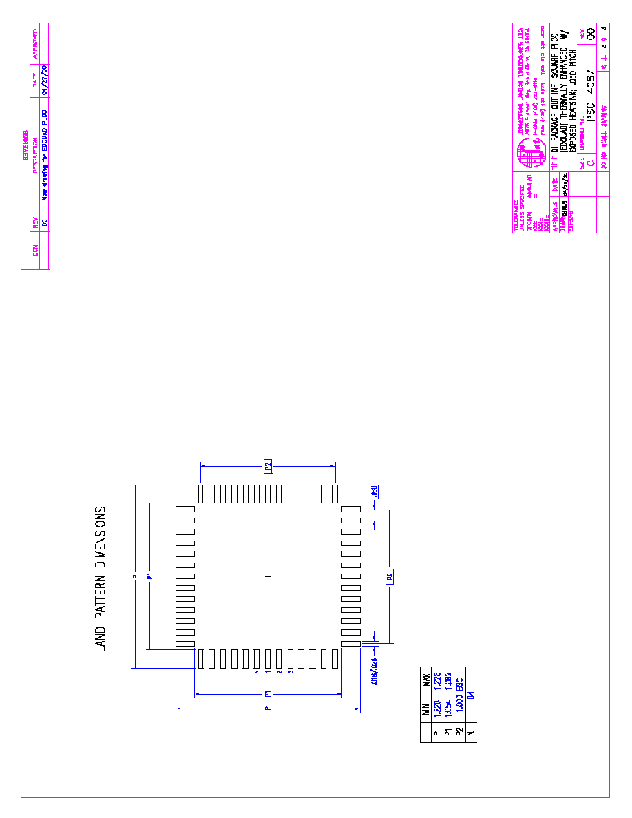
5.5 41
IDT79R3081 RISController
MILITARY AND COMMERCIAL TEMPERATURE RANGES
ORDERING INFORMATION
IDT
XXXXX
Device Type
XX
Speed
X
Package
≠
X
Process/
Temp. Range
Blank
B
M
DL
FD
J
PF
20
25
33
40
50
79R3081
79R3081E
79RV3081
79RV3081E
Commercial Temperature Range
Compliant to MIL-STD-883, Class B
Military Temperature Range Only
84-Pin Thermally Enhanced
84-lead Cavity-down Flatpack with
Integral Thermal Slug
84-lead PLCC
100-lead TQFP
20.0MHz
25.0MHz
33.33MHz
40.0MHz
50.0MHz
No TLB; V
CC
= 5V
With TLB; V
CC
= 5V
No TLB; V
CC
= 3.3V
With TLB; V
CC
= 3.3V
2889 drw 37
5V Only
VALID COMBINATIONS
IDT 79R3081 (E) ≠ 20, 25, 33, 40, 50
DL Package
79RV3081 (E) ≠ 20, 25, 33
PF Package
79RV3081(E) ≠ 20, 25, 33, 40
DL Package
79R3081E ≠ 20, 25 (FDB/FDM)
FD Package Only
(5V Only)