 | –≠–ª–µ–∫—Ç—Ä–æ–Ω–Ω—ã–π –∫–æ–º–ø–æ–Ω–µ–Ω—Ç: 7M9519 | –°–∫–∞—á–∞—Ç—å:  PDF PDF  ZIP ZIP |
1
1999 Integrated Device Technology, Inc.
DSC-4266/2
©
JULY 1999
Common Bus CPU Card (C3)
Family for 64-bit MIPS
Processors
PRELIMINARY
IDT7M9516 IDT7M9521
IDT7M9518 IDT7M9522
IDT7M9519 IDT7M9523
IDT7M9520
4266 dwg 01
FEATURES:
∑ Supports IDT Common Bus CPU Card (C3) electrical and
mechanical specifications.
∑ C3 Card family supports IDT 64bit MIPS family including R4650,
R4700, R64475, R5000, R64575 for easy scaling of performance.
∑ Low profile, mezzanine form-factor. Ideal daughtercard for:
≠
Compact PCI
≠
VME
≠
Ethernet / ATM switches
∑ Utilizes SAMTEC CLP connectors
≠
100 pin Conn. A: part number: CLP-150-02-L-D-PA
≠
96 pin Conn. B: part number: CLP-148-02-L-D-PA
∑ Onboard clock generation circuitry for processor/system
clocks
∑ Onboard processor reset and configuration circuitry.
∑ 5V Tolerance
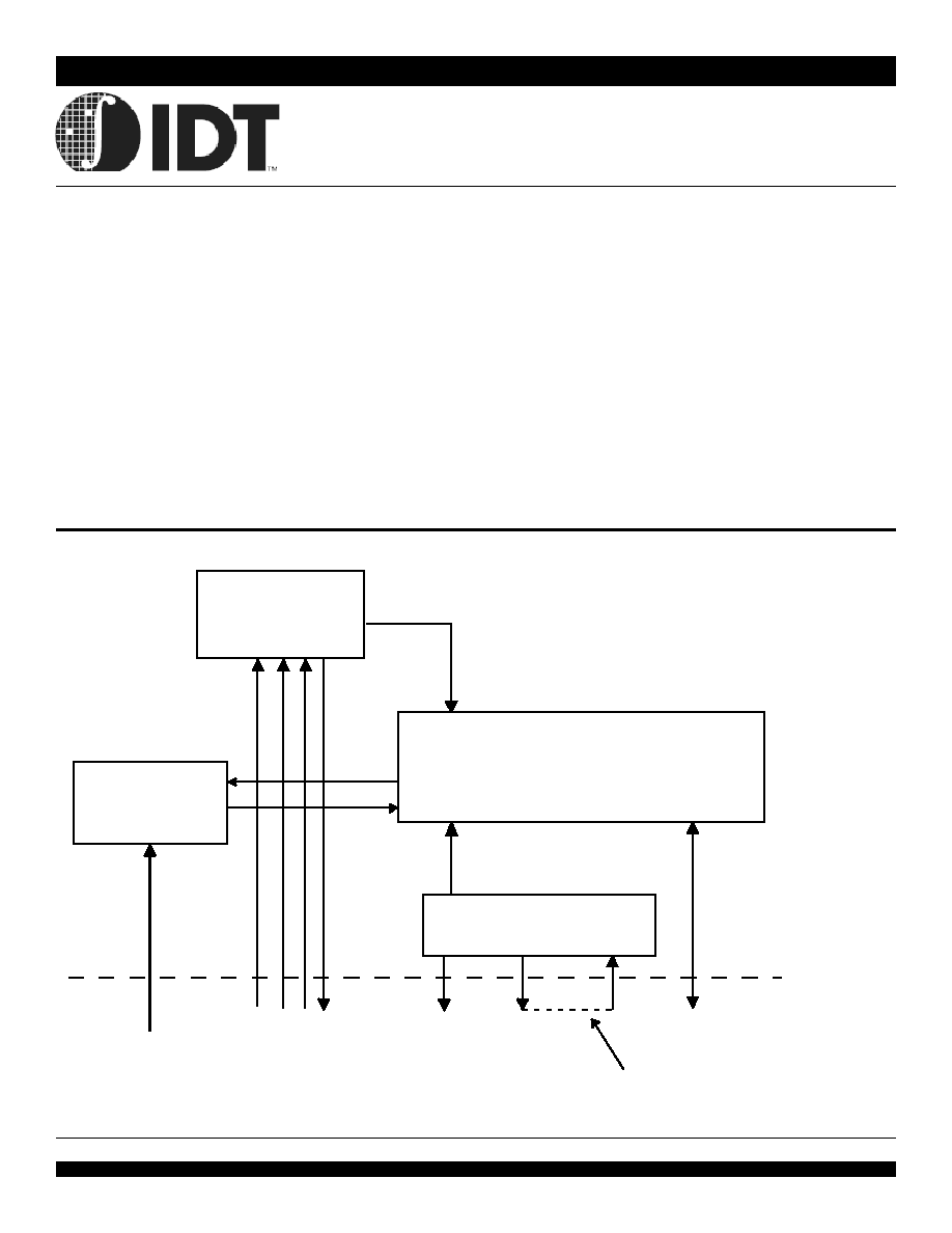
FUNCTIONAL BLOCK DIAGRAM
DESCRIPTION:
The C3 family are CPU mezzanine daughtercards based on IDT's MIPS
processors. The C3 Card family is designed to replace the CPU and specific
support circuitry around the CPU in a system design. The goal of the C3 is
to provide the system designer a seamless hardware migration path
through IDT's family of 64-bit MIPS processors(R4650, R4700, R64475,
R5000, R64575), and to simplify the overall system implementation require-
ments of those processors.
Each of the above processors has a unique pin configuration/package;
therefore, a system designer would normally be required to implement a
unique board design for each of the processors. The goal of the C3 is to
eliminate the differences between these processors at the system interface
level, and to allow the system designer to implement a single baseboard
design which will support C3 cards featuring the R4650, R4700, R64475,
R5000, R64575 or future processors.
Reset
Generation
Configuration
Logic
MIPS CPU
SyncO ut
SyncIn
SysAD , etc.
C LO C K
G EN ER ATIO N
System
C locks
C 3/System
Boundary
SyncO ut m ust be tied to
SyncIn for proper operation
C onfiguration
Inputs
2
1999 Integrated Device Technology, Inc.
DSC-4266/2
©
IDT
IDT7M9516/18/19/20/21/22/23
CLOCK GENERATION
The C3 provides nine clock outputs that are associated with system bus clock
generation, as well as a 20MHz clock output and a 24MHz clock output. The
ten bus clock outputs consist of nine identical buffered system clocks and one
dedicated output for processor to system clock synchronization. The system
clocks - SysCLK(0:8) - are provided to drive devices on the system bus, as well
as other devices that need to operate at the system clock frequency. The
processor synchronization clock output (SyncOut) must be connected to the
processor synchronization clock input (SyncIn) through a delay path that
matches the delay path of the system clocks to ensure proper operation of the
C3 in the system. The 20MHz and 24MHz clocks are provided for system
peripherals that have fixed frequency requirements.
WATCHDOG TIMER
The watchdog timer input (WDStrb pin B-172) of the C3 must be strobed
periodically to prevent the watchdog timer output (WDO* pin B-173) from being
asserted. If the input is not strobed within 1 second of the previous strobe, the
output will be asserted. Note that if the watchdog timer functionality is not required,
these pins can be left unconnected.
5V TOLERANCE CIRCUITRY
5V tolerance is provided by running the signals through bus switches.
All inputs and I/O's are 5V tolerant except for SYNCIN. The input voltage
on SYNCIN must not exceed VCC3 + 0.3V. (Not available on 7M9521 and
7M9522).
BOARD OVERVIEW
The C3 processor cards consist of the following functional blocks: 64bit
MIPS CPU, clock generation circuitry for the processor/system clocks,
processor reset and configuration circuitry, and an optional L2 cache
subsystem.
RESET CONFIGURATION
The C3 contains on board reset generation logic that provides all of the
reset requirements of the processor. This reset logic handles all Power On
Reset requirements, as well as handling two system hard reset sources
(S_HardRST*, A_HardRST*) and a system soft reset source (SoftRST*).
In addition, the reset logic of the C3 also provides a reset output (RSTOut*)
to the system that is asserted whenever there is a processor hard reset.
C3 CONFIGURATION
The C3 is configured through a set of static configuration inputs. The
configuration inputs are used for both C3 clock configuration and proces-
sor configuration. The clock configuration inputs are used to set the
system bus clock frequency and the CPU core to system bus clock
multiplier. The processor configuration inputs are used to configure the
following: endianess (big/little), drive strength (83%/100%), internal timer
(enabled/disabled), write type (R4X00/pipelined) and block write data rate
(D/Dx/Dxx/Dxxx).
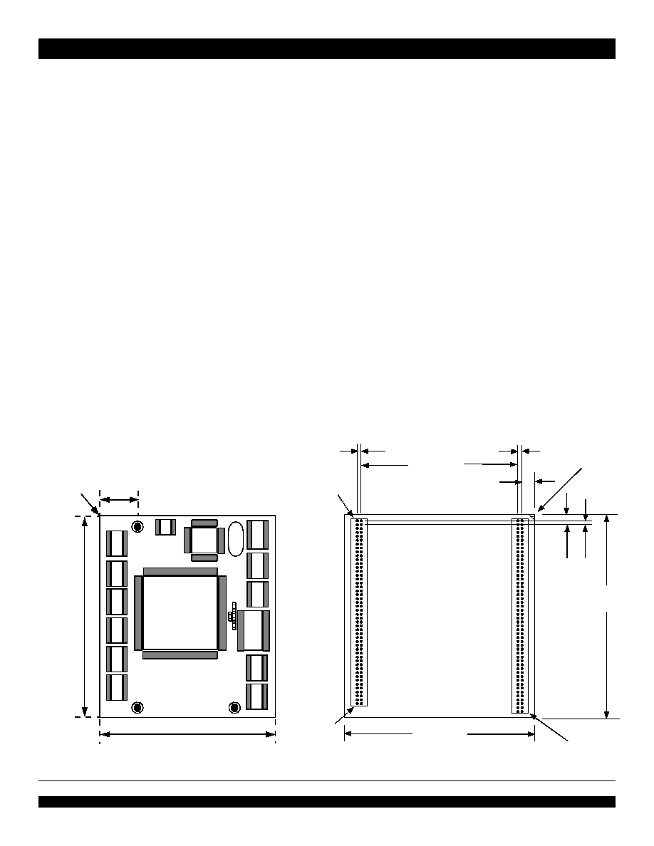
NOTES:
1. All dimensions in inches.
2. Actual component placement may differ from those shown in the diagram.
4266 dwg 2A
4266 dwg 05
TOP VIEW
BOTTOM VIEW
PACKAGE DIMENSIONS
M IP S
C P U
F
S
T
F
S
T
F
S
T
F
S
T
F
S
T
F
S
T
F
S
T
F
S
T
F
S
T
F
S
T
XT
A
L
CLK
G
E
N
P A L
CLK
D
R
V
2 .4 5
2.
60
0 .5 0
P in 1
P in 1
. 0 5 0
.0 5 0
2 . 4 5 0
(+ / - 0 . 0 1 0 )
.1 6 9 R E F
. 0 7 5 R E F
2 .0 1 3
.0 5 0 T Y P
2 . 6 0 0
(+ / - 0 .0 1 0 )
P in 5 0
P in 1 4 9
P in 1 9 6

3
1999 Integrated Device Technology, Inc.
DSC-4266/2
©
IDT
IDT7M9516/18/19/20/21/22/23
PINOUT
(1)
4266 dwg 03
NOTE:
1. The pinout of the C3 card is from a top view.
2. This pin is not connected (NC) on the 7M9516.
1
2
3
4
5
6
7
8
9
10
11
12
13
14
15
16
17
18
19
20
21
22
23
24
25
26
27
28
29
30
31
32
33
34
35
36
37
38
39
40
41
42
43
44
45
46
47
48
49
50
51
52
53
54
55
56
57
58
59
60
61
62
63
64
65
66
67
68
69
70
71
72
73
74
75
76
77
78
79
80
81
82
83
84
85
86
87
88
89
90
91
92
93
94
95
96
97
98
99
100
C onnector A
V C C 5
S ysA D (10)
S ysA D (41)
S ysC M D (6)
G N D
S ys A D(8)
C lkM ult(0)
C lkM ult(1)
G N D
S ysA D P (4)
R S V D
S ysC M D (4)
G N D
S ys A D(7)
S ysA D (38)
W rR dy*
G N D
S ys A D(5)
S ysA D (36)
G N D
S ysC M D (1)
S ys A D(3)
G N D
S ysA D (34)
IN T 5*
S ysA D (33)
G N D
S ys A D(0)
IN T 2*
G N D
S ysA D (48)
S ysA D (17)
G N D
IN T 0*
S ysA D (50)
G N D
S ysA D (19)
S ysA D (20)
G N D
S ysA D (21)
R E LE A S E *
G N D
R dR dy*
S ysA D (54)
G N D
S ysA D (23)
N MI*
G N D
S ysA D (24)
V C C 5
V C C 5
S ysC M D (7)
G N D
S ysA D( 9)
S ysA D (4 0)
S ysC M D (5)
S cT C E *
A _H ard R st*
C lkM ult(2)
S ysA DC (0)
S ysA D (3 9)
G N D
R S V D
S ysC M D (3)
S ysA D( 6)
V C C 3
S ysA D (3 7)
S ysC M D (2)
S ysA D( 4)
G N D
S ysA D (3 5)
S ysC M D (0)
S ysA D( 2)
V C C 3
IN T 4*
S ysA D( 1)
S ysA D (3 2)
V C C 3
IN T 3*
S ysA D (1 6)
IN T 1*
V C C 3
S ysA D (4 9)
S ysA D (1 8)
V alidIn*
G N D
R S V D
S ysA D (5 1)
S ysA D (5 2)
V C C 3
V alidO ut*
R S V D
G N D
S ysA D (5 3)
S ysA D (2 2)
S ysA D (5 5)
V C C 3
S ysA D P (2)
S ysA D P (6)
V C C 5
1 0 1
1 0 2
1 0 3
1 0 4
1 0 5
1 0 6
1 0 7
1 0 8
1 0 9
1 1 0
1 1 1
1 1 2
1 1 3
1 1 4
1 1 5
1 1 6
1 1 7
1 1 8
1 1 9
1 2 0
1 2 1
1 2 2
( 2 )
1 2 3
1 2 4
1 2 5
1 2 6
1 2 7
1 2 8
1 2 9
1 3 0
1 3 1
1 3 2
1 3 3
1 3 4
1 3 5
1 3 6
1 3 7
1 3 8
1 3 9
1 4 0
1 4 1
1 4 2
1 4 3
1 4 4
1 4 5
1 4 6
1 4 7
1 4 8
1 4 9
1 5 0
1 5 1
1 5 2
1 5 3
1 5 4
1 5 5
1 5 6
1 5 7
1 5 8
1 5 9
1 6 0
1 6 1
1 6 2
1 6 3
1 6 4
1 6 5
1 6 6
1 6 7
1 6 8
1 6 9
1 7 0
1 7 1
1 7 2
1 7 3
1 7 4
1 7 5
1 7 6
1 7 7
1 7 8
1 7 9
1 8 0
1 8 1
1 8 2
1 8 3
1 8 4
1 8 5
1 8 6
1 8 7
1 8 8
1 8 9
1 9 0
1 9 1
1 9 2
1 9 3
1 9 4
1 9 5
1 9 6
V C C 5
S _ H a r d R s t*
O u tD r v
S o ftR s t*
G N D
2 0 M H z O u t
G N D
2 4 M h z O u t
G N D
S y s A D ( 4 2 )
S y s A D ( 1 1 )
S y s A D ( 1 2 )
V C C 3
S y s A D ( 1 3 )
B lk W r ( 0 )
B lk W r ( 1 )
V C C 3
S y s A D ( 1 4 )
S y s A D ( 1 5 )
S y s A D P ( 1 )
G N D
S y s C lk ( 8 )
E n d i a n
V C C 3
S y n c In
V C C 3
S y s C lk ( 1 )
V C C 3
S y n c O u t
V C C 3
S y s C L K ( 3 )
V C C 3
S y s C L K ( 5 )
V C C 3
S y s C L K ( 7 )
V C C 3
S y s A D P ( 7 )
G N D
S y s A D ( 6 3 )
S y s A D ( 6 2 )
S y s A D ( 2 9 )
V C C 3
S y s A D ( 2 8 )
S y s A D ( 2 7 )
S y s A D ( 2 6 )
G N D
S y s A D ( 5 6 )
V C C 5
V C C 5
C L K F r e q ( 0 )
C L K F r e q ( 1 )
C L K F r e q ( 2 )
S c D O E *
G N D
S c W o r d ( 0 )
S c W o r d ( 1 )
L 2 _ H it
S y s C M D ( 8 )
G N D
S y s A D ( 4 3 )
S y s A D ( 4 4 )
S y s A D ( 4 5 )
G N D
T i m e r E n *
W r T y p e
R S V D
G N D
S y s A D ( 4 6 )
S y s A D ( 4 7 )
S y s A D P ( 5 )
G N D
W D _ S tr b
W D O *
R s tO u t*
G N D
S y s C L K ( 0 )
G N D
S y s C L K ( 2 )
G N D
S y s C L K ( 4 )
G N D
S y s C L K ( 6 )
G N D
E x tR e q *
S y s A D C ( 3 )
S y s A D ( 3 1 )
S y s A D ( 3 0 )
G N D
S y s A D ( 6 1 )
S y s A D ( 6 0 )
S y s A D ( 5 9 )
G N D
S y s A D ( 5 8 )
S y s A D ( 5 7 )
S y s A D ( 2 5 )
V C C 5
C onnector B

4
1999 Integrated Device Technology, Inc.
DSC-4266/2
©
IDT
IDT7M9516/18/19/20/21/22/23
PIN DEFINITIONS
Signal Name
Signal Definition
Type
Description
SysAD(63:0)
System (CPU)
I/O
64-bit multiplexed address/data bus. This bus is driven by the C3 during the address
Address/Data Bus
phase (SysCMD(8)=0) of a bus transaction. Valid data is driven by the C3 during the
data phase (SysCMD(8)=1) for writes when ValidOut* is asserted. The C3 receives
data on this bus during the data phase for reads when ValidIn* is sampled low.
SysADP(7:0)
SysAD Parity
I/O
Even parity is generated during the data phase for writes. Even parity is checked during
the data phase for reads if SysCMD(4) is low. Timing and valid sample windows match
SysAD(63:0). SysADP(0) is assosciated with SysAD(7:0), SysADP(1) is associated
withSysAD(15:8).
SysCMD(8:0)
System (CPU)
I/O
This is the 9-bit processor command bus.
command/data
SysCLK(8:0)
System (CPU)
Output
Nine identical clocks for devices residing on the C3 processor bus. All processor
Clocks
transitions/transactions are referenced with respect to these clocks.
SyncOut
Synchronization
Output
The C3 system clock generator synchronization output must be connected to SyncIn
Clock Output
through an interconnect scheme that matches that used on SysCLK(8:0).
SyncIn
Synchronization
Input
C3 system clock generator synchronization input. This pin must be connected to
Clock Input
SyncOut for the C3 to operate.
RdRdy*
Read Ready
Input
This pin is driven low by the system to indicate that the system is ready to accept a C3 read
request.
WrRdy*
Write Ready
Input
This pin is driven low by the system to indicate that the system is ready to accept a C3
write request.
ValidOut*
Valid Output
Output
This pin is driven low by the C3 to indicate that it is driving a valid address/data on the SysAD,
SysADP and SysCMD busses.
ValidIn*
Valid Input
Input
This pin in driven low by the system to indicate that it is presenting valid address/data on
the SysAD, SysADP and SysCMD busses.
Endian
Endian
Config
Endian configuration input.
Input
0=big, 1=little
OutDrv
Output Drive
Config
Output drive strength configuration input.
Input
0=100%, 1=83%
TimerEn*
Timer Enable
Config
CPU internal timer interrupt enable configuration input.
Input
0=enable timer, 1=disable timer
WrType
Write Type
Config
Write Type configuration input.
Input
0=R4X00 compatible, 1=Pipelined
ClockMult(2:0)
Clock Multiplier
Config
000=x2
Input
001=x3
010=x4
011=x5
100-101=reserved
110=SmartClock mode 0 (max CPU core frequency)
111=SmartClock mode 1(max CPU bus frequency)
BlkWr(1:0)
Block Write
Config
Block Write data rate
Input
00=DDDD
01=DxDxDxD
10=DxxDxxDxxD
11=DxxxDxxxDxxxD
RELEASE*
Release Interface
Output
This pin is driven low to signal to the requesting device that the system interface is available.
ExtReq*
External Request
Intput
This pin is driven low to request the use of the system interface.
4266 tbl 01

5
1999 Integrated Device Technology, Inc.
DSC-4266/2
©
IDT
IDT7M9516/18/19/20/21/22/23
PIN DEFINITIONS (CONTINUED)
Signal Name
Signal Definition
Type
Description
ClkFreq(2:0)
SysCLK
Config
In normal mode these inputs specify the system bus clock frequency. In SmartClock
Frequency
Input
mode, these inputs specify the maximum system clock frequency.
000=45MHz (includes 43.75/44)
100=75MHz
001=50MHz
101=83MHz
010=60MHz (includes 58.33)
110=90MHz
011=66MHz
111=100MHz
INT*(5:0)
Interrupts
Input
General processor interrupts.
NMI*
Non-Maskable
Input
Non-maskable interrupt
Interrupt
SoftRST*
Soft Reset
Input
Asserting this input causes a processor soft (or warm) reset.
S_HardRST*
Synchronous
Input
Asserting this input causes a processor hard (or cold) reset.
Hard Reset
A_HardRST*
Asynchronous
Input
Asserting this input causes a processor hard (or cold) reset.
Hard Reset
RSTOut*
Reset Output
Output
This pin is asserted by the C3 to reset system logic. This output is asserted during
power-on reset, and whenever HardRST* is asserted.
WDO*
Watch Dog
Output
This pin asserted by the C3 whenever there is a timeout of the watchdog
Output
timer.
WD_Strb
Watch Dog
Input
This pin must be strobed periodically by the system to prevent the Strobe watchdog timer
from timing out.
L2_HIT
L2 Cache Hit
Output
This pin indicates to the system that a hit has occurred in the on board
(ScMatch)
L2 cache. This pin is a no connect on the 7M9516/18/19/20/23.
ScDOE*
Secondary
Input
Only used when a secondary cache is implemented with the R5K internal
Cache Data
cache controller. This pin is a no connect on the 7M9516/18/19/20/23.
OE*
ScWord(1:0)
Secondary
I/O
Only used when a secondary cache is implemented with the R5K internal
Cache Word
cache controller
ScTCE*
Secondary Cache
Output
This pin indicates to the system when the L2 cache controller of the R5K is accessing the
Tag Chip Enable
Tag RAM. This pin is driven high by the 7M9516/18/19/20/23.
20MHz Out
20MHz Clock
Output
20MHz Clock
24MHz Out
24MHz Clock
Output
24MHz Clock
GND
Ground
Supply
System Ground
VCC3
+3.3V
Supply
System 3.3V Supply
VCC5
+5V
Supply
System 5V Supply
4266 tbl 03
ENVIRONMENTAL
Temp. (∞C)
Humidity
(1)
Condition
Min
Max
Min
Max
Operating
0
55
20%
80%
Non-Op.
-10
60
10%
90%
Storage
-25
60
10%
90%
NOTE:
1. Non-Condensing
4266 tbl 02
6
CORPORATE HEADQUATERS
for SALES:
for Tech Support:
2975 Stender Way
800-345-7015
408-988-5647
Santa Clara, CA 95054
fax: 408-492-8674
ssdhelp@idt.com
www.idt.com
The IDT logo is a registered trademark of Integrated Device Technology, Inc.
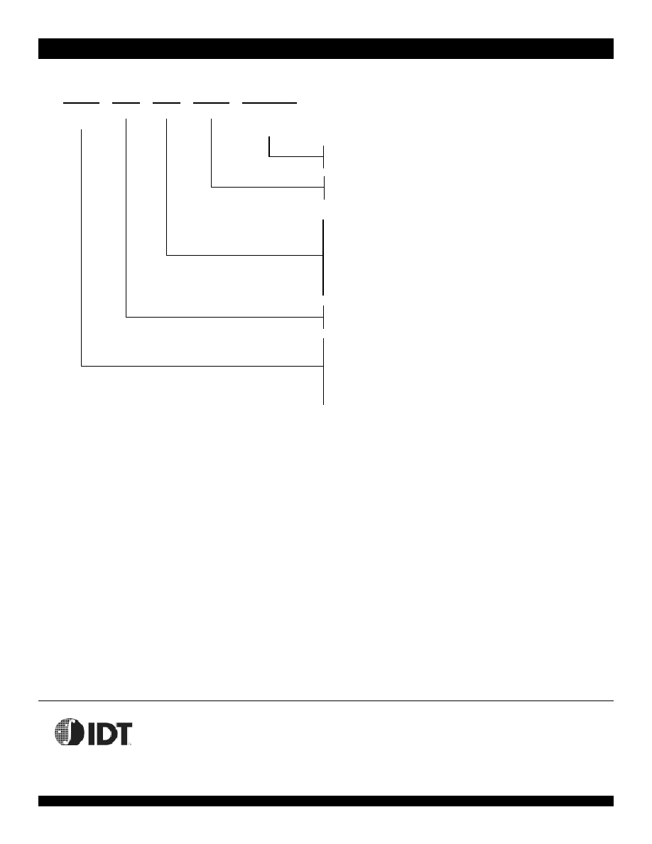
ORDERING INFORMATION
4266 dwg 04
X
P ower
X
S peed
X
P ackage
X
P rocess/
Tem perature
Range
B lank
Com m ercial (0∞C to +70∞C)
M
196-pin M ezzanine C onnector
333
300
250
200
180
175
150
100
S S tandard
Pow er
X XX X X
Device
Type
7M 9516
7M 9518
7M 9519
7M 9520
7M 9521
7M 9522
7M 9523
Com m on B us CP U (C 3) C ard for R4700
Com m on B us CP U (C 3) C ard for R4650
Com m on B us CP U (C 3) C ard for R64475
Com m on B us CP U (C 3) C ard for R5000
Com m on B us CP U (C 3) C ard for R5000 w /512K L2 Cache
Com m on B us CP U (C 3) C ard for R5000 w /1M B L2 Cache
Com m on B us CP U (C 3) C ard for R64575
ID T
P rocessor Core Frequency (M H z)
7M 9523 Only
7M 9523 Only
E xcluding 7M 9516 and 7M 9518
E xcluding 7M 9516 and 7M 9523
7M 9516 Only
E xcluding 7M 9519 and 7M 9523
7M 9516/18 O nly