©2003 Integrated Device Technology, Inc.
JANUARY 2003
DSC-4083/05
1
Features
x
x
x
x
x
High density 3 megabit 3.3V static RAM
x
x
x
x
x
Low profile 119 lead, 14mm x 22mm
BGA (Ball Grid Array)
x
x
x
x
x
Fast RAM access times: 10,12,15ns
x
x
x
x
x
Single 3.3V power supply
x
x
x
x
x
Multiple Vcc & GND pins for maximum noise immunity
x
x
x
x
x
Inputs/outputs directly LVTTL compatible
x
x
x
x
x
Commercial (0
O
C to +70
O
C) Industrial (-40
O
C to +85
O
C)
temperature options
≠ Commercial: 10 / 12 / 15 ns
≠ Industrial: 12 / 15 ns
Description
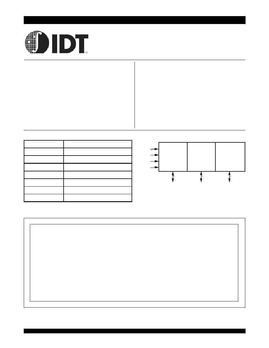
The IDT7MMV4101 is a three megabit static RAM constructed on an
multilayer laminate substrate using three 3.3V, 128K x 8 (IDT71V124)
static RAMS encapsulated in a Ball Grid Array (BGA).
The IDT7MMV4101 is packaged in a plastic BGA. The BGA configu-
ration allows 119 leads to be placed on a package 14mm by 22mm. At a
maximum of 3.5mm high, this low-profile surface mount package is ideal
for ultra dense systems.
All inputs and outputs of the IDT7MMV4101 are LVTTL compatible and
operate from a single 3.3V supply. Full asynchronous circuitry requires
no clocks or refresh for operation and provides equal access and cycle
times for ease of use.
Pin Names
Pin Configuration
Functional Block Diagram
1
2
3
4
5
6
7
A
NC
A0
A1
A2
A3
A4
NC
B
NC
A5
A6
CS
A7
A8
NC
C
I/O12
NC
NC
NC
NC
NC
I/O0
D
I/O13
VCC
GND
GND
GND
VCC
I/O1
E
I/O14
GND
VCC
GND
VCC
GND
I/O2
F
I/O15
VCC
GND
GND
GND
VCC
I/O3
G
I/O16
GND
VCC
GND
VCC
GND
I/O4
H
I/O17
VCC
GND
GND
GND
VCC
I/O5
NC
GND
VCC
GND
VCC
GND
NC
K
I/O18
VCC
GND
GND
GND
VCC
I/O6
L
I/O19
GND
VCC
GND
VCC
GND
I/O7
M
I/O20
VCC
GND
GND
GND
VCC
I/O8
N
I/O21
GND
VCC
GND
VCC
GND
I/O9
P
I/O22
VCC
GND
GND
GND
VCC
I/O10
R
I/O23
NC
NC
NC
NC
NC
I/O11
T
NC
A9
A10
WE
A11
A12
NC
U
NC
A13
A14
OE
A15
A16
NC
J
,
4083 drw 02
128K x 8
SRAM
8
I/O
0-7
8
I/O
8-15
8
I/O
16-23
17
A
0-16
128K x 8
SRAM
128K x 8
SRAM
CS
WE
OE
,
4083 drw 01
128K x 24 Three Megabit
3.3V CMOS Static RAM
IDT7MMV4101
I/O
0
-
23
Data Inputs/Outputs
A
0
-
16
Addresses
CS
Chip Select
WE
Write Enable
OE
Output Enable
V
CC
Power
GND
Ground
NC
No Connect
4083 tbl 01
Top View
2
IDT7MMV4101
128K x 24 Three Megabit 3.3V CMOS Static RAM Commercial and Industrial Temperature Ranges
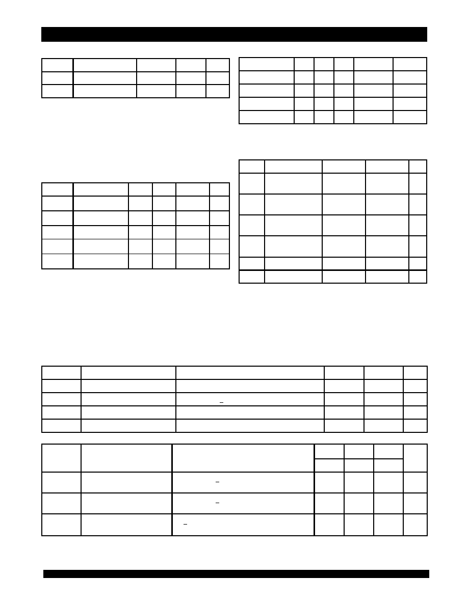
Truth Table
Absolute Maximum Ratings
(1)
Recommended DC Operating
Conditions
Capacitance
(T
A
= +25∞C, f = 1.0MHz)
DC Electrical Characteristics
(V
CC
= 3.3V ±10%)
NOTES:
1. Commercial temperature only, Vcc = -5% to +10%.
NOTE:
1. This parameter is guaranteed by design but not tested.
Symbol
Parameter
(1)
Conditions
Max.
Unit
C
IN
Input Capacitance
V
IN
= 3dV
20
pF
C
I/O
I/O Capacitance
V
OUT
= 3dV
10
pF
4083 tbl 02
NOTES:
1. For 7MMV4101S10BG only.
2. For all speed grades except 7MMV4101S10BG.
3. V
IL
(min) = ≠1.5V for pulse width less than 5ns, once per cycle.
4. V
IH
(max) =
V
cc + 1.5V for pulse width less than 5ns, once per cycle.
Symbol
Parameter
Min.
Typ.
Max.
Unit
V
CC
(1)
Supply Voltage
3.15
3.3
3.6
V
V
CC
(2)
Supply Voltage
3.0
3.3
3.6
V
GND
Ground
0
0
0
V
V
IH
Input High Voltage
2.0
____
V
CC
+ 0.3
(4)
V
V
IL
Input Low Voltage
-0.3
(3)
____
0.8
V
4083 tbl 03
Mode
CS
OE
WE
I/O
Power
Standby
H
X
X
High-Z
Standby
Read
L
L
H
DATA
OUT
Active
Write
L
X
L
DATA
IN
Active
Outputs Disabled
L
H
H
High-Z
Active
4083 tbl 04
NOTES:
1. Stresses greater than those listed under ABSOLUTE MAXIMUM RATINGS
may cause permanent damage to the device. This is a stress rating only
and functional operation of the device at these or any other conditions above
those indicated in the operational sections of this specification is not implied.
Exposure to absolute maximum rating conditions for extended periods may
affect reliability.
Symbol
Rating
Commercial
Industrial
Unit
V
CC
Supply Voltage
Relative to GND
-0.5 to +4.6
-0.5 to +4.6
V
V
TERM
Terminal Voltage with
Respect to GND
-0.5 to V
CC
+0.5 -0.5 to V
CC
+0.5
V
T
A
Operating
Temperature
0 to +70
-40 to +85
∞C
T
BIAS
Temperature
Under Bias
-10 to +85
-10 to +85
∞C
T
STG
Storage Temperature
-55 to +125
-55 to +125
∞C
I
OUT
DC Output Current
50
50
mA
4083 tbl 05
Symbol
Parameter
Test Condition
Min.
Max.
Unit
II
LI
I
Input Leakage Current
V
CC
= Max., V
IN
= GND to V
CC
____
15
µ
A
II
LO
I
Output Leakage Current
V
CC
= Max.,
CS > V
IH
, V
OUT
= GND to V
CC,
____
5
µ
A
V
OL
Output Low Voltage
I
OL
= 8mA, V
CC
= Min.
____
0.4
V
V
OH
Output High Voltage
I
OH
= -4mA, V
CC
= Min.
2.4
____
V
4083 tbl 06
-10
(1)
-12
-15
Symbol
Parameter
Test Condition
Max.
Max.
Max.
Unit
I
CC
Dynamic Operating
Current
V
CC
= Max.,
CS < V
IL
,
f = f
MAX
, Outputs Open
295
275
255
mA
I
SB
Standby Power
Supply Current
V
CC
= Max.,
CS > V
IH
,
f = f
MAX
, Outputs Open
95
85
85
mA
I
SB1
Full Standby Power
Supply Current
CS > V
CC
- 0.2V, f =0
V
IN
> V
CC
- 0.2V or < 0.2V
10
10
10
mA
4083 tbl 07
6.42
IDT7MMV4101
128K x 24 Three Megabit 3.3V CMOS Static RAM Commercial and Industrial Temperature Ranges
3
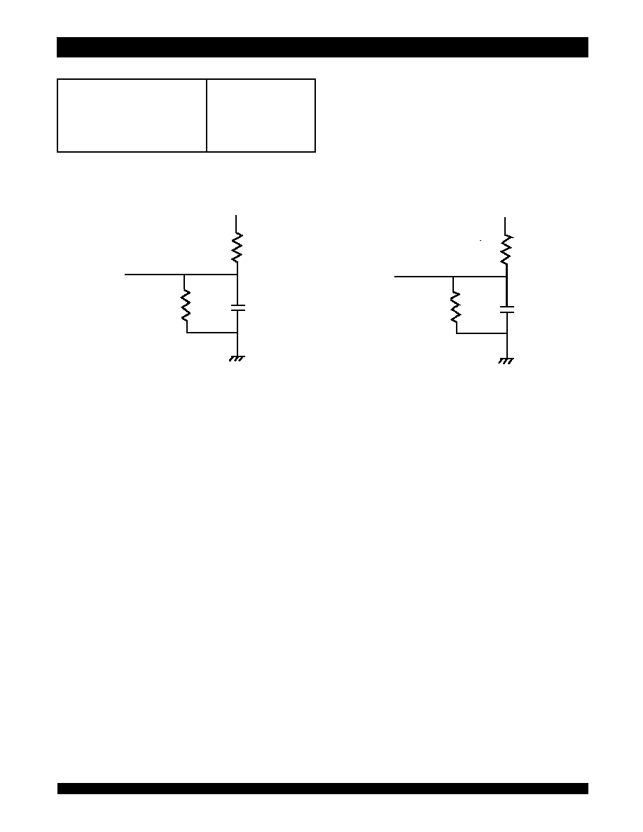
AC Test Conditions
5 pF*
+3.3 V
298
30 pF
DATA
OUT
216
+3.3 V
298
DATA
216
OUT
4083 drw 03
,
Input Pulse Levels
Input Rise/Fall Times
Input Timing Reference Levels
Output Reference Levels
Output Load
GND to 3.0V
3ns
1.5V
1.5V
See Figures 1 and 2
4083 tbl 08
Figure 1. Output Load
Figure 2. Output Load
(for t
OLZ
, t
OHZ
, t
CHZ
, t
CLZ
, t
WHZ
, t
OW
)
* Includes scope and jig.
4
IDT7MMV4101
128K x 24 Three Megabit 3.3V CMOS Static RAM Commercial and Industrial Temperature Ranges
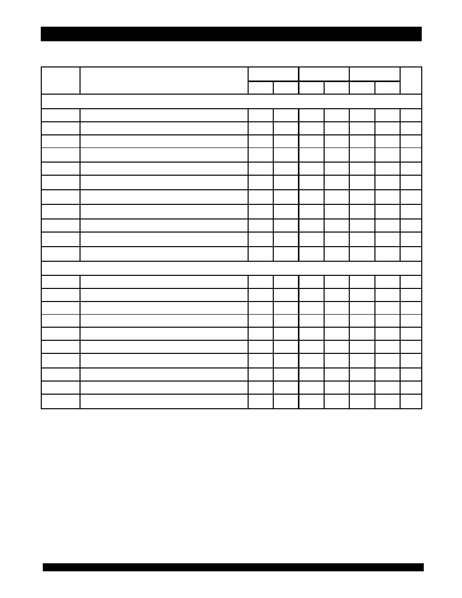
AC Electrical Characteristics
(2)
(V
CC
= 3.3V ±10%)
-10
(3)
-12
-15
Symbol
Parameter
Min.
Max.
Min.
Max.
Min.
Max.
Unit
Read Cycle
t
RC
Read Cycle Time
10
____
12
____
15
____
ns
t
AA
Address Access Time
____
10
____
12
____
15
ns
t
ACS
Chip Select Access Time
____
10
____
12
____
15
ns
t
CLZ
(1)
Chip Select to Output in Low-Z
3
____
3
____
3
____
ns
t
OE
Output Enable to Output Valid
____
4
____
6
____
7
ns
t
OLZ
(1)
Output Enable to Output in Low-Z
0
____
0
____
0
____
ns
t
CHZ
(1)
Chip Deselect to Output in High-Z
____
5
____
6
____
7
ns
t
OHZ
(1)
Output Disable to Output in High-Z
____
5
____
6
____
7
ns
t
OH
Output Hold from Address Change
3
____
3
____
3
____
ns
t
PU
(1)
Chip Select to Power-Up Time
0
____
0
____
0
____
ns
t
PD
(1)
Chip Deselect to Power-Down Time
____
10
____
12
____
15
ns
Write Cycle
t
WC
Write Cycle Time
10
____
12
____
15
____
ns
t
CW
Chip Select to End-of-Write
8
____
10
____
12
____
ns
t
AW
Address Valid to End-of-Write
8
____
10
____
12
____
ns
t
AS
Address Set-up Time
0
____
0
____
0
____
ns
t
WP
Write Pulse Width
8
____
10
____
12
____
ns
t
WR
Write Recovery Time
0
____
0
____
0
____
ns
t
WHZ
(1)
Write Enable to Output in High-Z
____
5
____
5
____
5
ns
t
DW
Data to Write Time Overlap
6
____
6
____
7
____
ns
t
DH
Data Hold from Write Time
0
____
0
____
0
____
ns
t
OW
(1)
Output Active from End-of-Write
3
____
3
____
3
____
ns
4083 tbl 09
NOTES:
1. This parameter is guaranteed by design but not tested.
2. These specifications are for the individual 71V124 Static RAMs.
3. Commercial temperature only, V
CC
= -5% to +10%.
6.42
IDT7MMV4101
128K x 24 Three Megabit 3.3V CMOS Static RAM Commercial and Industrial Temperature Ranges
5
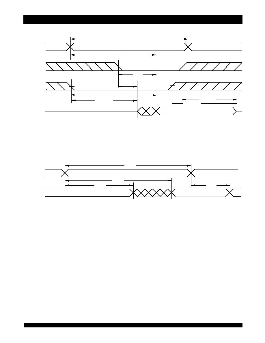
Timing Waveform of Read Cycle No. 1
(1)
Timing Waveform of Read Cycle No. 2
(1,2,4)
NOTES:
1.
WE is HIGH for Read Cycle.
2. Device is continuously selected,
CS is LOW.
3. Address must be valid prior to or coincident with the later of
CS transition LOW; otherwise t
AA
is the limiting parameter.
4.
OE is LOW.
5. Transition is measured ±200mV from steady state.
DATA
OUT
ADDRESS
4083 drw 05
t
RC
t
AA
t
OH
t
OH
DATA
OUT
VALID
PREVIOUS DATA
OUT
VALID
.
ADDRESS
4083 drw 04
OE
CS
DATA
OUT
(5)
(5)
(5)
(5)
DATA
OUT
VALID
HIGH IMPEDANCE
t
AA
t
RC
t
OE
t
ACS
t
OLZ
t
CHZ
t
CLZ
(3)
t
OHZ
.
,
6
IDT7MMV4101
128K x 24 Three Megabit 3.3V CMOS Static RAM Commercial and Industrial Temperature Ranges
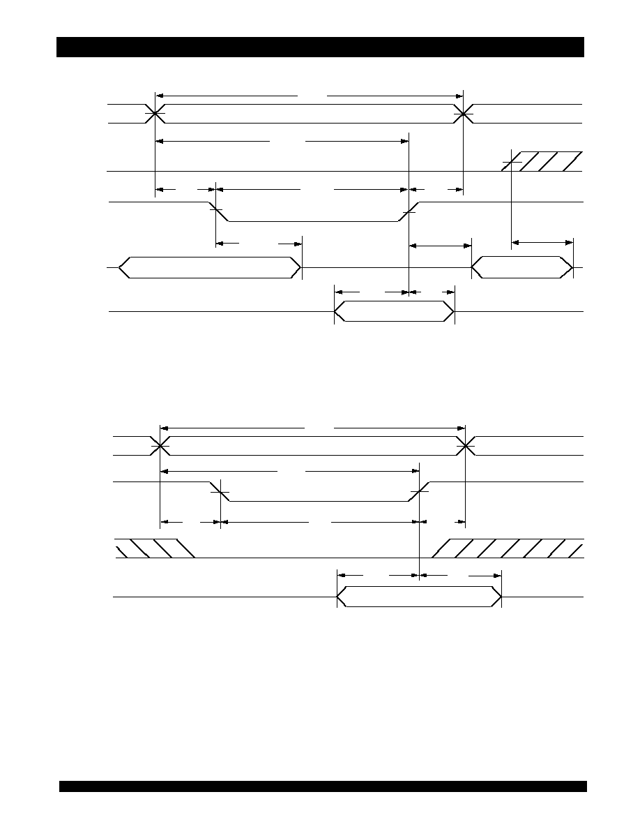
Timing Waveform of Write Cycle No. 1 (WE Controlled Timing)
(1,4,5)
Timing Waveform of Write Cycle No. 2 (CS Controlled Timing)
(1, 4)
CS
ADDRESS
DATA
IN
4083 drw 07
t
AW
t
WC
t
CW
t
AS
t
WR
t
DW
t
DH
DATA
IN
VALID
WE
(3)
.
NOTES:
1. A write occurs during the overlap of a LOW
CS and a LOW WE.
2.
OE is continuously HIGH. During a WE controlled write cycle with OE LOW, t
WP
must be greater than or equal to t
WHZ
+ t
DW
to allow the I/O drivers to turn off and
data to be placed on the bus for the required t
DW
. If
OE is HIGH during a WE controlled write cycle, this requirement does not apply and the minimum write pulse
is the specified t
WP
.
3. During this period, I/O pins are in the output state, and input signals must not be applied.
4. If the
CS LOW transition occurs simultaneously with or after the WE LOW transition, the outputs remain in a high impedance state. CS must be active during the t
CW
write period.
5. Transition is measured ±200mV from steady state.
ADDRESS
CS
WE
DATA
OUT
DATA
IN
4083 drw 06
(3)
DATA
IN
VALID
HIGH IMPEDANCE
t
WC
t
AW
t
AS
t
WHZ
t
WP
t
CHZ
t
OW
t
DW
t
DH
t
WR
(4)
(4)
.
(5)
(5)
(5)
6.42
IDT7MMV4101
128K x 24 Three Megabit 3.3V CMOS Static RAM Commercial and Industrial Temperature Ranges
7
Package Dimensions
Ordering Information
NOTES:
1. All dimensions are in mm.
X
Power
X
Speed
X
Package
X
Process/
Temperature
Range
XXXXX
Device
Type
IDT
I
Blank
BG
10
12
15
S
7MMV4101
119 lead BGA (Ball Grid Array)
Speed in Nanoseconds
Commercial Temp Only
Commercial and Industrial Temp
Commercial and Industrial Temp
Standard Power
3 Megabit Static RAM
Industrial (-40∞C to +85∞C)
Commercial (0∞C to +70∞C)
4083 drw 09
,
14.00 + 0.1
22.0 + 0.1
2.15 Nom.
2.36 Max
A
B
C
D
E
F
G
H
I
J
K
L
M
N
O
P
Q
7
6
5
4
3
2
1
1.27 Typ
7.62 Ref
20.32 Ref
TOP VIEW
BOTTOM VIEW
0.84
REF
3.19
REF
,
4083 drw 08

8
IDT7MMV4101
128K x 24 Three Megabit 3.3V CMOS Static RAM Commercial and Industrial Temperature Ranges
CORPORATE HEADQUARTERS
for SALES:
for Tech Support:
2975 Stender Way
800-345-7015 or 408-727-6116
sramhelp@idt.com
Santa Clara, CA 95054
fax:408-492-8674
800 544-7726, x4033
www.idt.com
The IDT logo is a registered trademark of Integrated Device Technology, Inc.
Datasheet History
09/18/00
Add datasheet history
Pg. 2
Reduce I
CC
, I
SB
, and I
SB1
to reflect K step die shrink
01/07/03
Changed datasheet from Prelininary to final release