 | –≠–ª–µ–∫—Ç—Ä–æ–Ω–Ω—ã–π –∫–æ–º–ø–æ–Ω–µ–Ω—Ç: 82P2284 | –°–∫–∞—á–∞—Ç—å:  PDF PDF  ZIP ZIP |

Quad T1/E1/J1 Long Haul /
Short Haul Transceiver
IDT82P2284
Version -
April 25, 2003
2975 Stender Way, Santa Clara, Califormia 95054
Telephone: (800) 345-7015 ∑ TWX: 910-338-2070 ∑ FAX: (408) 492-8674
Printed in U.S.A.
© 2001 Integrated Device Technology, Inc.

DISCLAIMER
Integrated Device Technology, Inc. reserves the right to make changes to its products or specifications at any time, without notice, in order to improve design or performance and to supply the best pos-
sible product. IDT does not assume any responsibility for use of any circuitry described other than the circuitry embodied in an IDT product. The Company makes no representations that circuitry
described herein is free from patent infringement or other rights of third parties which may result from its use. No license is granted by implication or otherwise under any patent, patent rights or other
rights, of Integrated Device Technology, Inc.
LIFE SUPPORT POLICY
Integrated Device Technology's products are not authorized for use as critical components in life support devices or systems unless a specific written agreement pertaining to such intended use is exe-
cuted between the manufacturer and an officer of IDT.
1. Life support devices or systems are devices or systems which (a) are intended for surgical implant into the body or (b) support or sustain life and whose failure to perform, when properly used in
accordance with instructions for use provided in the labeling, can be reasonably expected to result in a significant injury to the user.
2. A critical component is any components of a life support device or system whose failure to perform can be reasonably expected to cause the failure of the life support device or system, or to affect its
safety or effectiveness.

Table of Contents
i
April 25, 2003
Table of Contents
*Notice: The information in this document is subject to change without notice
FEATURES ........................................................................................................................................................................ 1
APPLICATIONS ................................................................................................................................................................ 1
BLOCK DIAGRAM ............................................................................................................................................................ 2
1 PIN ASSIGNMENT ........................................................................................................................................................... 3
2 PIN DESCRIPTION ........................................................................................................................................................... 4
3 FUNCTIONAL DESCRIPTION ........................................................................................................................................ 12
3.1 T1 / E1 / J1 MODE SELECTION .................................................................................................................................................................. 14
3.2 RECEIVER IMPEDANCE MATCHING ......................................................................................................................................................... 15
3.3 ADAPTIVE EQUALIZER .............................................................................................................................................................................. 17
3.4 DATA SLICER .............................................................................................................................................................................................. 17
3.5 CLOCK AND DATA RECOVERY ................................................................................................................................................................ 17
3.6 RECEIVE JITTER ATTENUATOR ............................................................................................................................................................... 18
3.7 DECODER .................................................................................................................................................................................................... 19
3.7.1 Line Code Rule ............................................................................................................................................................................... 19
3.7.1.1 T1 / J1 Mode .................................................................................................................................................................... 19
3.7.1.2 E1 Mode ........................................................................................................................................................................... 19
3.7.2 Decode Error Detection ................................................................................................................................................................. 19
3.7.2.1 T1 / J1 Mode .................................................................................................................................................................... 19
3.7.2.2 E1 Mode ........................................................................................................................................................................... 19
3.7.3 LOS Detection ................................................................................................................................................................................ 20
3.8 FRAME PROCESSOR ................................................................................................................................................................................. 23
3.8.1 T1/J1 Mode ...................................................................................................................................................................................... 23
3.8.1.1 Synchronization Searching ............................................................................................................................................... 23
3.8.1.1.1 Super Frame (SF) Format ............................................................................................................................. 23
3.8.1.1.2 Extended Super Frame (ESF) Format ........................................................................................................... 24
3.8.1.1.3 T1 Digital Multiplexer (DM) Format (T1 only) ................................................................................................ 25
3.8.1.1.4 Switch Line Carrier - 96 (SLC-96) Format (T1 only) ...................................................................................... 26
3.8.1.2 Error Event And Out Of Synchronization Detection .......................................................................................................... 27
3.8.1.2.1 Super Frame (SF) Format ............................................................................................................................. 27
3.8.1.2.2 Extended Super Frame (ESF) Format ........................................................................................................... 27
3.8.1.2.3 T1 Digital Multiplexer (DM) Format (T1 only) ................................................................................................ 27
3.8.1.2.4 Switch Line Carrier - 96 (SLC-96) Format (T1 only) ...................................................................................... 27
3.8.1.3 Overhead Extraction (T1 Mode SLC-96 Format Only) ..................................................................................................... 28
3.8.1.4 Interrupt Summary ............................................................................................................................................................ 28
3.8.2 E1 Mode .......................................................................................................................................................................................... 30
3.8.2.1 Synchronization Searching ............................................................................................................................................... 32
3.8.2.1.1 Basic Frame .................................................................................................................................................. 32
3.8.2.1.2 CRC Multi-Frame ........................................................................................................................................... 33
3.8.2.1.3 CAS Signaling Multi-Frame ........................................................................................................................... 34
3.8.2.2 Error Event And Out Of Synchronization Detection .......................................................................................................... 34
3.8.2.2.1 Out Of Basic Frame Synchronization ............................................................................................................ 35
3.8.2.2.2 Out Of CRC Multi-Frame Synchronization .................................................................................................... 35
3.8.2.2.3 Out Of CAS Signaling Multi-Frame Synchronization ..................................................................................... 35
3.8.2.3 Overhead Extraction ......................................................................................................................................................... 35
3.8.2.3.1 International Bit Extraction ............................................................................................................................. 35
3.8.2.3.2 Remote Alarm Indication Bit Extraction ......................................................................................................... 35

IDT82P2284
QUAD T1/E1/J1 LONG HAUL / SHORT HAUL TRANSCEIVER
Table of Contents
ii
April 25, 2003
*Notice: The information in this document is subject to change without notice
3.8.2.3.3 National Bit Extraction ................................................................................................................................... 35
3.8.2.3.4 National Bit Codeword Extraction .................................................................................................................. 35
3.8.2.3.5 Extra Bit Extraction ........................................................................................................................................ 35
3.8.2.3.6 Remote Signaling Multi-Frame Alarm Indication Bit Extraction ..................................................................... 35
3.8.2.3.7 Sa6 Code Detection Per ETS 300 233 .......................................................................................................... 35
3.8.2.4 V5.2 Link .......................................................................................................................................................................... 36
3.8.2.5 Interrupt Summary ............................................................................................................................................................ 36
3.9 PERFORMANCE MONITOR ........................................................................................................................................................................ 38
3.9.1 T1/J1 Mode ...................................................................................................................................................................................... 38
3.9.2 E1 Mode .......................................................................................................................................................................................... 40
3.10 ALARM DETECTOR .................................................................................................................................................................................... 42
3.10.1 T1/J1 Mode ...................................................................................................................................................................................... 42
3.10.2 E1 Mode .......................................................................................................................................................................................... 44
3.11 HDLC RECEIVER ......................................................................................................................................................................................... 45
3.11.1 HDLC Channel Configuration ........................................................................................................................................................ 45
3.11.2 Two HDLC Modes ........................................................................................................................................................................... 45
3.11.2.1 HDLC Mode ...................................................................................................................................................................... 45
3.11.2.2 SS7 Mode ......................................................................................................................................................................... 47
3.12 BIT-ORIENTED MESSAGE RECEIVER (T1/J1 ONLY) .............................................................................................................................. 49
3.13 INBAND LOOPBACK CODE DETECTOR (T1/J1 ONLY) ........................................................................................................................... 49
3.14 ELASTIC STORE BUFFER .......................................................................................................................................................................... 50
3.15 RECEIVE CAS/RBS BUFFER ..................................................................................................................................................................... 50
3.15.1 T1/J1 Mode ...................................................................................................................................................................................... 50
3.15.2 E1 Mode .......................................................................................................................................................................................... 51
3.16 RECEIVE PAYLOAD CONTROL ................................................................................................................................................................. 53
3.17 RECEIVE SYSTEM INTERFACE ................................................................................................................................................................. 55
3.17.1 T1/J1 Mode ...................................................................................................................................................................................... 55
3.17.1.1 Receive Clock Master Mode ............................................................................................................................................ 55
3.17.1.1.1 Receive Clock Master Full T1/J1 Mode ......................................................................................................... 55
3.17.1.1.2 Receive Clock Master Fractional T1/J1 Mode ............................................................................................... 56
3.17.1.2 Receive Clock Slave Mode .............................................................................................................................................. 56
3.17.1.3 Receive Multiplexed Mode ............................................................................................................................................... 57
3.17.1.4 Offset ................................................................................................................................................................................ 57
3.17.1.5 Output On RSDn/MRSDA(MRSDB) & RSIGn/MRSIGA(MRSIGB) .................................................................................. 59
3.17.2 E1 Mode .......................................................................................................................................................................................... 60
3.17.2.1 Receive Clock Master Mode ............................................................................................................................................ 60
3.17.2.1.1 Receive Clock Master Full E1 Mode ............................................................................................................. 60
3.17.2.1.2 Receive Clock Master Fractional E1 Mode ................................................................................................... 60
3.17.2.2 Receive Clock Slave Mode .............................................................................................................................................. 60
3.17.2.3 Receive Multiplexed Mode ............................................................................................................................................... 61
3.17.2.4 Offset ................................................................................................................................................................................ 61
3.17.2.5 Output On RSDn/MRSDA(MRSDB) & RSIGn/MRSIGA(MRSIGB) .................................................................................. 61
3.18 TRANSMIT SYSTEM INTERFACE .............................................................................................................................................................. 62
3.18.1 T1/J1 Mode ...................................................................................................................................................................................... 62
3.18.1.1 Transmit Clock Master Mode ............................................................................................................................................ 62
3.18.1.1.1 Transmit Clock Master Full T1/J1 Mode ........................................................................................................ 63
3.18.1.1.2 Transmit Clock Master Fractional T1/J1 Mode .............................................................................................. 63
3.18.1.2 Transmit Clock Slave Mode ............................................................................................................................................. 63
3.18.1.3 Transmit Multiplexed Mode .............................................................................................................................................. 64
3.18.1.4 Offset ................................................................................................................................................................................ 65
3.18.2 E1 Mode .......................................................................................................................................................................................... 67
3.18.2.1 Transmit Clock Master Mode ............................................................................................................................................ 67
3.18.2.1.1 Transmit Clock Master Full E1 Mode ............................................................................................................ 67
3.18.2.1.2 Transmit Clock Master Fractional E1 Mode .................................................................................................. 67

IDT82P2284
QUAD T1/E1/J1 LONG HAUL / SHORT HAUL TRANSCEIVER
Table of Contents
iii
April 25, 2003
*Notice: The information in this document is subject to change without notice
3.18.2.2 Transmit Clock Slave Mode ............................................................................................................................................. 67
3.18.2.3 Transmit Multiplexed Mode .............................................................................................................................................. 68
3.18.2.4 Offset ................................................................................................................................................................................ 68
3.19 TRANSMIT PAYLOAD CONTROL .............................................................................................................................................................. 69
3.20 FRAME GENERATOR ................................................................................................................................................................................. 70
3.20.1 Generation ...................................................................................................................................................................................... 70
3.20.1.1 T1 / J1 Mode .................................................................................................................................................................... 70
3.20.1.1.1 Super Frame (SF) Format ............................................................................................................................. 70
3.20.1.1.2 Extended Super Frame (ESF) Format ........................................................................................................... 70
3.20.1.1.3 T1 Digital Multiplexer (DM) Format (T1 only) ................................................................................................ 70
3.20.1.1.4 Switch Line Carrier - 96 (SLC-96) Format (T1 only) ...................................................................................... 70
3.20.1.1.5 Interrupt Summary ......................................................................................................................................... 71
3.20.1.2 E1 Mode ........................................................................................................................................................................... 72
3.20.1.2.1 Interrupt Summary ......................................................................................................................................... 73
3.20.2 HDLC Transmitter .......................................................................................................................................................................... 75
3.20.2.1 HDLC Channel Configuration ........................................................................................................................................... 75
3.20.2.2 Two HDLC Modes ............................................................................................................................................................ 75
3.20.2.2.1 HDLC Mode ................................................................................................................................................... 75
3.20.2.2.2 SS7 Mode ...................................................................................................................................................... 75
3.20.2.3 Interrupt Summary ............................................................................................................................................................ 76
3.20.2.4 Reset ................................................................................................................................................................................ 76
3.20.3 Automatic Performance Report Message (T1/J1 Only) .............................................................................................................. 77
3.20.4 Bit-Oriented Message Transmitter (T1/J1 Only) .......................................................................................................................... 78
3.20.5 Inband Loopback Code Generator (T1/J1 Only) .......................................................................................................................... 78
3.20.6 All `Zero's & All `One's ................................................................................................................................................................... 78
3.20.7 Change Of Frame Alignment ......................................................................................................................................................... 78
3.21 TRANSMIT BUFFER .................................................................................................................................................................................... 79
3.22 ENCODER .................................................................................................................................................................................................... 79
3.22.1 Line Code Rule ............................................................................................................................................................................... 79
3.22.1.1 T1/J1 Mode ...................................................................................................................................................................... 79
3.22.1.2 E1 Mode ........................................................................................................................................................................... 79
3.22.2 BPV Error Insertion ........................................................................................................................................................................ 79
3.22.3 All `One's Insertion ........................................................................................................................................................................ 79
3.23 TRANSMIT JITTER ATTENUATOR ............................................................................................................................................................ 80
3.24 WAVEFORM SHAPER / LINE BUILD OUT ................................................................................................................................................. 81
3.24.1 Preset Waveform Template ........................................................................................................................................................... 81
3.24.1.1 T1/J1 Mode ...................................................................................................................................................................... 81
3.24.1.2 E1 Mode ........................................................................................................................................................................... 81
3.24.2 Line Build Out (LBO) (T1 Only) ..................................................................................................................................................... 82
3.24.3 User-Programmable Arbitrary Waveform .................................................................................................................................... 82
3.25 LINE DRIVER ............................................................................................................................................................................................... 89
3.26 TRANSMITTER IMPEDANCE MATCHING ................................................................................................................................................. 90
3.27 TESTING AND DIAGNOSTIC FACILITIES ................................................................................................................................................. 91
3.27.1 PRBS Generator / Detector ........................................................................................................................................................... 91
3.27.1.1 Pattern Generator ............................................................................................................................................................. 91
3.27.1.2 Pattern Detector ............................................................................................................................................................... 91
3.27.2 Loopback ........................................................................................................................................................................................ 92
3.27.2.1 System Loopback ............................................................................................................................................................. 92
3.27.2.1.1 System Remote Loopback ............................................................................................................................ 92
3.27.2.1.2 System Local Loopback ................................................................................................................................ 92
3.27.2.2 Payload Loopback ............................................................................................................................................................ 92
3.27.2.3 Local Digital Loopback 1 .................................................................................................................................................. 92
3.27.2.4 Remote Loopback ............................................................................................................................................................ 92
3.27.2.5 Local Digital Loopback 2 .................................................................................................................................................. 92

IDT82P2284
QUAD T1/E1/J1 LONG HAUL / SHORT HAUL TRANSCEIVER
Table of Contents
iv
April 25, 2003
*Notice: The information in this document is subject to change without notice
3.27.2.6 Analog Loopback .............................................................................................................................................................. 92
3.27.3 G.772 Non-Intrusive Monitoring .................................................................................................................................................... 92
3.28 INTERRUPT SUMMARY .............................................................................................................................................................................. 95
4 OPERATION .................................................................................................................................................................... 96
4.1 POWER-ON SEQUENCE ............................................................................................................................................................................. 96
4.2 RESET .......................................................................................................................................................................................................... 96
4.3 RECEIVE / TRANSMIT PATH POWER DOWN ........................................................................................................................................... 96
4.4 MICROPROCESSOR INTERFACE ............................................................................................................................................................. 97
4.4.1 SPI Mode ......................................................................................................................................................................................... 97
4.4.2 Parallel Microprocessor Interface ................................................................................................................................................ 98
4.5 INDIRECT REGISTER ACCESS SCHEME ................................................................................................................................................. 99
4.5.1 Indirect Register Read Access ..................................................................................................................................................... 99
4.5.2 Indirect Register Write Access ..................................................................................................................................................... 99
5 PROGRAMMING INFORMATION ................................................................................................................................. 100
5.1 REGISTER MAP ......................................................................................................................................................................................... 100
5.1.1 T1/J1 Mode .................................................................................................................................................................................... 100
5.1.1.1 Direct Register ................................................................................................................................................................ 100
5.1.1.2 Indirect Register ............................................................................................................................................................. 105
5.1.2 E1 Mode ........................................................................................................................................................................................ 106
5.1.2.1 Direct Register ................................................................................................................................................................ 106
5.1.2.2 Indirect Register ............................................................................................................................................................. 111
5.2 REGISTER DESCRIPTION ........................................................................................................................................................................ 113
5.2.1 T1/J1 Mode .................................................................................................................................................................................... 114
5.2.1.1 Direct Register ................................................................................................................................................................ 114
5.2.1.2 Indirect Register ............................................................................................................................................................. 216
5.2.2 E1 Mode ........................................................................................................................................................................................ 229
5.2.2.1 Direct Register ................................................................................................................................................................ 229
5.2.2.2 Indirect Register ............................................................................................................................................................. 332
6 IEEE STD 1149.1 JTAG TEST ACCESS PORT ........................................................................................................... 347
6.1 JTAG INSTRUCTIONS AND INSTRUCTION REGISTER (IR) .................................................................................................................. 348
6.2 JTAG DATA REGISTER ............................................................................................................................................................................ 349
6.2.1 Device Identification Register (IDR) ........................................................................................................................................... 349
6.2.2 Bypass Register (BYP) ................................................................................................................................................................ 349
6.2.3 Boundary Scan Register (BSR) ................................................................................................................................................... 349
6.3 TEST ACCESS PORT CONTROLLER ...................................................................................................................................................... 352
7 PHYSICAL AND ELECTRICAL SPECIFICATIONS ..................................................................................................... 355
7.1 ABSOLUTE MAXIMUM RATINGS ............................................................................................................................................................ 355
7.2 RECOMMENDED OPERATING CONDITIONS ......................................................................................................................................... 355
7.3 D.C. CHARACTERISTICS ......................................................................................................................................................................... 356
7.4 DIGITAL I/O TIMING CHARACTERISTICS ............................................................................................................................................... 357
7.5 CLOCK FREQUENCY REQUIREMENT .................................................................................................................................................... 357
7.6 T1/J1 LINE RECEIVER ELECTRICAL CHARACTERISTICS ................................................................................................................... 358
7.7 E1 LINE RECEIVER ELECTRICAL CHARACTERISTICS ........................................................................................................................ 359
7.8 T1/J1 LINE TRANSMITTER ELECTRICAL CHARACTERISTICS ............................................................................................................ 360
7.9 E1 LINE TRANSMITTER ELECTRICAL CHARACTERISTICS ................................................................................................................ 361
7.10 JITTER TOLERANCE ................................................................................................................................................................................ 362
7.10.1 T1/J1 Mode .................................................................................................................................................................................... 362
7.10.2 E1 Mode ........................................................................................................................................................................................ 363
7.11 JITTER TRANSFER ................................................................................................................................................................................... 364
7.11.1 T1/J1 Mode .................................................................................................................................................................................... 364
7.11.2 E1 Mode ........................................................................................................................................................................................ 365
7.12 MICROPROCESSOR TIMING SPECIFICATION ....................................................................................................................................... 366
7.12.1 Motorola Non-Multiplexed Mode ................................................................................................................................................. 366

IDT82P2284
QUAD T1/E1/J1 LONG HAUL / SHORT HAUL TRANSCEIVER
Table of Contents
v
April 25, 2003
*Notice: The information in this document is subject to change without notice
7.12.1.1 Read Cycle Specification ............................................................................................................................................... 366
7.12.1.2 Write Cycle Specification ................................................................................................................................................ 367
7.12.2 Intel Non-Multiplexed Mode ......................................................................................................................................................... 368
7.12.2.1 Read Cycle Specification ............................................................................................................................................... 368
7.12.2.2 Write Cycle Specification ................................................................................................................................................ 369
7.12.3 SPI Mode ....................................................................................................................................................................................... 370
ORDERING INFORMATION ......................................................................................................................................... 371

List of Tables
vi
April 25, 2003
List of Tables
*Notice: The information in this document is subject to change without notice
Table 1: Operating Mode Selection ........................................................................................................................................................................... 14
Table 2: Related Bit / Register In Chapter 3.1 ........................................................................................................................................................... 14
Table 3: Impedance Matching Value For The Receiver ............................................................................................................................................. 15
Table 4: Related Bit / Register In Chapter 3.2 ........................................................................................................................................................... 16
Table 5: Related Bit / Register In Chapter 3.3 & Chapter 3.4 .................................................................................................................................... 17
Table 6: Criteria Of Speed Adjustment Start .............................................................................................................................................................. 18
Table 7: Related Bit / Register In Chapter 3.6 ........................................................................................................................................................... 18
Table 8: Excessive Zero Error Definition ................................................................................................................................................................... 19
Table 9: LOS Condition In T1/J1 Mode ...................................................................................................................................................................... 21
Table 10: LOS Condition In E1 Mode .......................................................................................................................................................................... 21
Table 11: Related Bit / Register In Chapter 3.7 ........................................................................................................................................................... 22
Table 12: The Structure of SF ..................................................................................................................................................................................... 23
Table 13: The Structure of ESF ................................................................................................................................................................................... 24
Table 14: The Structure of T1 DM ............................................................................................................................................................................... 25
Table 15: The Structure of SLC-96 .............................................................................................................................................................................. 26
Table 16: Interrupt Source In T1/J1 Frame Processor ................................................................................................................................................ 28
Table 17: Related Bit / Register In Chapter 3.8.1 ........................................................................................................................................................ 29
Table 18: The Structure Of TS0 In CRC Multi-Frame .................................................................................................................................................. 33
Table 19: FAS/NFAS Bit/Pattern Error Criteria ............................................................................................................................................................ 34
Table 20: Interrupt Source In E1 Frame Processor ..................................................................................................................................................... 36
Table 21: Related Bit / Register In Chapter 3.8.2 ........................................................................................................................................................ 37
Table 22: Monitored Events In T1/J1 Mode ................................................................................................................................................................. 38
Table 23: Related Bit / Register In Chapter 3.9.1 ........................................................................................................................................................ 39
Table 24: Monitored Events In E1 Mode ..................................................................................................................................................................... 40
Table 25: Related Bit / Register In Chapter 3.9.2 ........................................................................................................................................................ 41
Table 26: RED Alarm, Yellow Alarm & Blue Alarm Criteria ......................................................................................................................................... 42
Table 27: Related Bit / Register In Chapter 3.10.1 ...................................................................................................................................................... 43
Table 28: Related Bit / Register In Chapter 3.10.2 ...................................................................................................................................................... 44
Table 29: Related Bit / Register In Chapter 3.11.1 ...................................................................................................................................................... 45
Table 30: Interrupt Summarize In HDLC Mode ........................................................................................................................................................... 46
Table 31: Related Bit / Register In Chapter 3.11.2 ...................................................................................................................................................... 48
Table 32: Related Bit / Register In Chapter 3.12 ......................................................................................................................................................... 49
Table 33: Related Bit / Register In Chapter 3.13 ......................................................................................................................................................... 49
Table 34: Related Bit / Register In Chapter 3.14 ......................................................................................................................................................... 50
Table 35: Related Bit / Register In Chapter 3.15 ......................................................................................................................................................... 52
Table 36: A-Law Digital Milliwatt Pattern ..................................................................................................................................................................... 53
Table 37: µ-Law Digital Milliwatt Pattern ..................................................................................................................................................................... 53
Table 38: Related Bit / Register In Chapter 3.16 ......................................................................................................................................................... 54
Table 39: Operating Modes Selection In T1/J1 Receive Path ..................................................................................................................................... 55
Table 40: Operating Modes Selection In E1 Receive Path .......................................................................................................................................... 60
Table 41: Related Bit / Register In Chapter 3.17 ......................................................................................................................................................... 61
Table 42: Operating Modes Selection In T1/J1 Transmit Path .................................................................................................................................... 62
Table 43: Operating Modes Selection In E1 Transmit Path ......................................................................................................................................... 67
Table 44: Related Bit / Register In Chapter 3.18 ......................................................................................................................................................... 68
Table 45: Related Bit / Register In Chapter 3.19 ......................................................................................................................................................... 69
Table 46: Related Bit / Register In Chapter 3.20.1.1 ................................................................................................................................................... 71
Table 47: E1 Frame Generation .................................................................................................................................................................................. 72
Table 48: Control Over E Bits ...................................................................................................................................................................................... 72

IDT82P2284
QUAD T1/E1/J1 LONG HAUL / SHORT HAUL TRANSCEIVER
List of Tables
vii
April 25, 2003
*Notice: The information in this document is subject to change without notice
Table 49: Interrupt Summary In E1 Mode .................................................................................................................................................................... 73
Table 50: Related Bit / Register In Chapter 3.20.1.2 ................................................................................................................................................... 74
Table 51: Related Bit / Register In Chapter 3.20.2.1 ................................................................................................................................................... 75
Table 52: Related Bit / Register In Chapter 3.20.2.2 ~ Chapter 3.20.2.4 .................................................................................................................... 76
Table 53: APRM Message Format .............................................................................................................................................................................. 77
Table 54: APRM Interpretation .................................................................................................................................................................................... 77
Table 55: Related Bit / Register In Chapter 3.20.3 ...................................................................................................................................................... 78
Table 56: Related Bit / Register In Chapter 3.20.4 & Chapter 3.20.5 .......................................................................................................................... 78
Table 57: Related Bit / Register In Chapter 3.20.6, Chapter 3.20.7 & Chapter 3.21 ................................................................................................... 79
Table 58: Related Bit / Register In Chapter 3.22 ......................................................................................................................................................... 79
Table 59: Related Bit / Register In Chapter 3.23 ......................................................................................................................................................... 80
Table 60: PULS[3:0] Setting In T1/J1 Mode ................................................................................................................................................................ 81
Table 61: LBO PULS[3:0] Setting In T1 Mode ............................................................................................................................................................. 82
Table 62: Transmit Waveform Value For E1 75
...................................................................................................................................................... 83
Table 63: Transmit Waveform Value For E1 120
.................................................................................................................................................... 83
Table 64: Transmit Waveform Value For T1 0~133 ft ................................................................................................................................................. 84
Table 65: Transmit Waveform Value For T1 133~266 ft ............................................................................................................................................. 84
Table 66: Transmit Waveform Value For T1 266~399 ft ............................................................................................................................................. 85
Table 67: Transmit Waveform Value For T1 399~533 ft ............................................................................................................................................. 85
Table 68: Transmit Waveform Value For T1 533~655 ft ............................................................................................................................................. 86
Table 69: Transmit Waveform Value For J1 0~655 ft .................................................................................................................................................. 86
Table 70: Transmit Waveform Value For DS1 0 dB LBO ............................................................................................................................................ 87
Table 71: Transmit Waveform Value For DS1 -7.5 dB LBO ........................................................................................................................................ 87
Table 72: Transmit Waveform Value For DS1 -15.0 dB LBO ...................................................................................................................................... 88
Table 73: Transmit Waveform Value For DS1 -22.5 dB LBO ...................................................................................................................................... 88
Table 74: Related Bit / Register In Chapter 3.24 ......................................................................................................................................................... 88
Table 75: Impedance Matching Value For The Transmitter ........................................................................................................................................ 90
Table 76: Related Bit / Register In Chapter 3.25 & Chapter 3.26 ................................................................................................................................ 90
Table 77: Related Bit / Register In Chapter 3.27.1 ...................................................................................................................................................... 91
Table 78: Related Bit / Register In Chapter 3.27.2 & Chapter 3.27.3 .......................................................................................................................... 94
Table 79: Related Bit / Register In Chapter 3.28 ......................................................................................................................................................... 95
Table 80: Parallel Microprocessor Interface ................................................................................................................................................................ 98
Table 81: Related Bit / Register In Chapter 4 .............................................................................................................................................................. 99
Table 82: IR Code ..................................................................................................................................................................................................... 348
Table 83: IDR ............................................................................................................................................................................................................ 349
Table 84: Boundary Scan (BS) Sequence ................................................................................................................................................................ 349
Table 85: TAP Controller State Description .............................................................................................................................................................. 352

List of Figures
viii
April 25, 2003
List of Figures
*Notice: The information in this document is subject to change without notice
Figure 1. 208-Pin PBGA (Top View) ............................................................................................................................................................................. 3
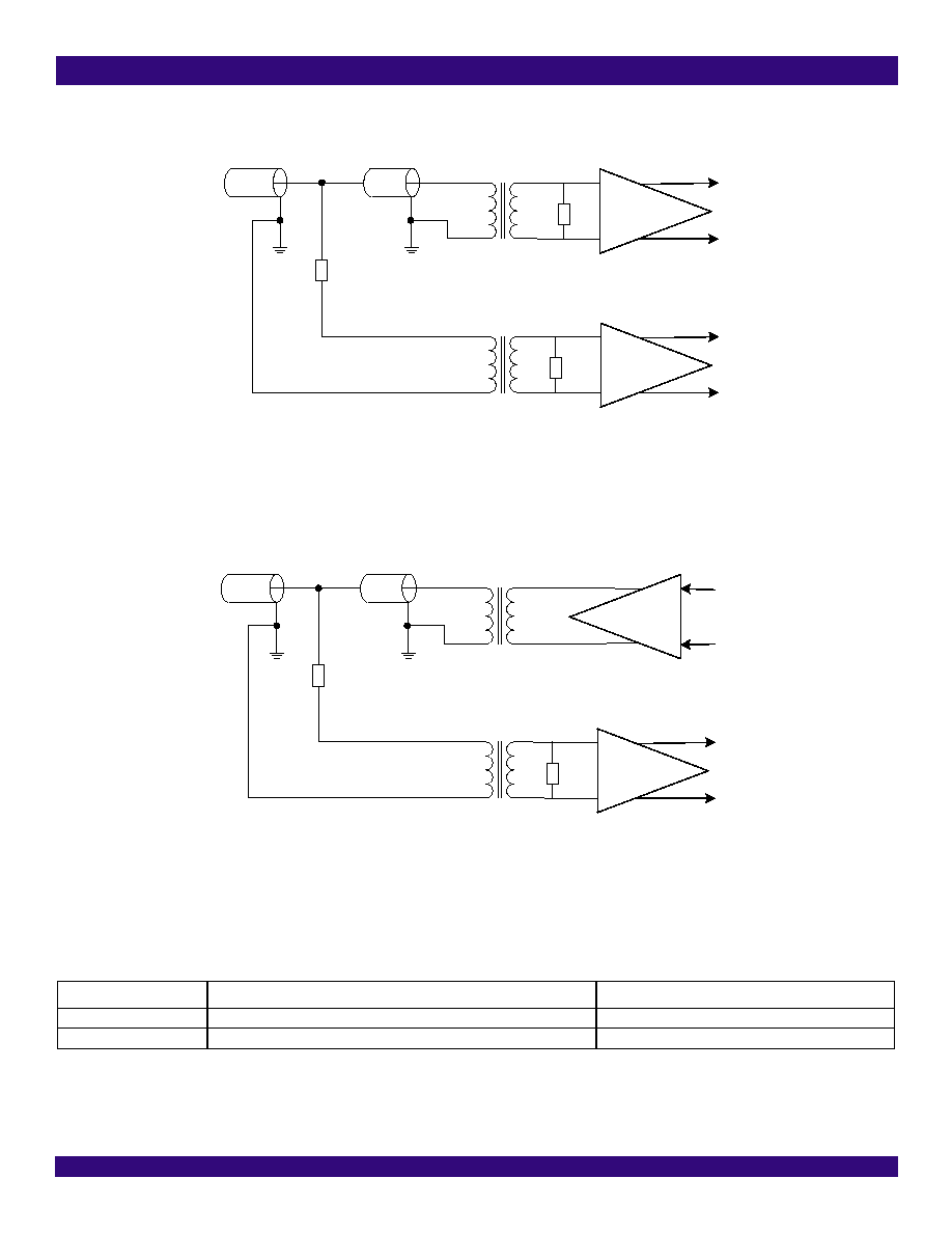
Figure 2. Receive / Transmit Line Circuit .................................................................................................................................................................... 15
Figure 3. Monitoring Receive Path .............................................................................................................................................................................. 16
Figure 4. Monitoring Transmit Path ............................................................................................................................................................................. 16
Figure 5. Jitter Attenuator ............................................................................................................................................................................................ 18
Figure 6. AMI Bipolar Violation Error ........................................................................................................................................................................... 20
Figure 7. B8ZS Excessive Zero Error ......................................................................................................................................................................... 20
Figure 8. HDB3 Code Violation & Excessive Zero Error ............................................................................................................................................. 20
Figure 9. E1 Frame Searching Process ...................................................................................................................................................................... 31
Figure 10. Basic Frame Searching Process ................................................................................................................................................................ 32
Figure 11. TS16 Structure Of CAS Signaling Multi-Frame .......................................................................................................................................... 34
Figure 12. Standard HDLC Packet .............................................................................................................................................................................. 45
Figure 13. Overhead Indication In The FIFO ............................................................................................................................................................... 46
Figure 14. Standard SS7 Packet ................................................................................................................................................................................. 47
Figure 15. Signaling Output In T1/J1 Mode ................................................................................................................................................................. 51
Figure 16. Signaling Output In E1 Mode ...................................................................................................................................................................... 51
Figure 17. T1/J1 To E1 Format Mapping - G.802 Mode .............................................................................................................................................. 56
Figure 18. T1/J1 To E1 Format Mapping - One Filler Every Four Channels Mode ..................................................................................................... 56
Figure 19. T1/J1 To E1 Format Mapping - Continuous Channels Mode ..................................................................................................................... 57
Figure 20. No Offset When FE = 1 & DE = 1 In Receive Path .................................................................................................................................... 58
Figure 21. No Offset When FE = 0 & DE = 0 In Receive Path .................................................................................................................................... 58
Figure 22. No Offset When FE = 0 & DE = 1 In Receive Path .................................................................................................................................... 59
Figure 23. No Offset When FE = 1 & DE = 0 In Receive Path .................................................................................................................................... 59
Figure 24. E1 To T1/J1 Format Mapping - G.802 Mode .............................................................................................................................................. 63
Figure 25. E1 To T1/J1 Format Mapping - One Filler Every Four Channels Mode ..................................................................................................... 63
Figure 26. E1 To T1/J1 Format Mapping - Continuous Channels Mode ..................................................................................................................... 64
Figure 27. No Offset When FE = 1 & DE = 1 In Transmit Path ................................................................................................................................... 65
Figure 28. No Offset When FE = 0 & DE = 0 In Transmit Path ................................................................................................................................... 65
Figure 29. No Offset When FE = 0 & DE = 1 In Transmit Path ................................................................................................................................... 66
Figure 30. No Offset When FE = 1 & DE = 0 In Transmit Path ................................................................................................................................... 66
Figure 31. DSX-1 Waveform Template ........................................................................................................................................................................ 81
Figure 32. T1/J1 Pulse Template Measurement Circuit .............................................................................................................................................. 81
Figure 33. E1 Waveform Template .............................................................................................................................................................................. 81
Figure 34. E1 Pulse Template Measurement Circuit ................................................................................................................................................... 81
Figure 35. G.772 Non-Intrusive Monitor ...................................................................................................................................................................... 93
Figure 36. Hardware Reset When Powered-Up .......................................................................................................................................................... 96
Figure 37. Hardware Reset In Normal Operation ........................................................................................................................................................ 96
Figure 38. Read Operation In SPI Mode ..................................................................................................................................................................... 97
Figure 39. Write Operation In SPI Mode ...................................................................................................................................................................... 97
Figure 40. JTAG Architecture .................................................................................................................................................................................... 347
Figure 41. JTAG State Diagram ................................................................................................................................................................................ 354
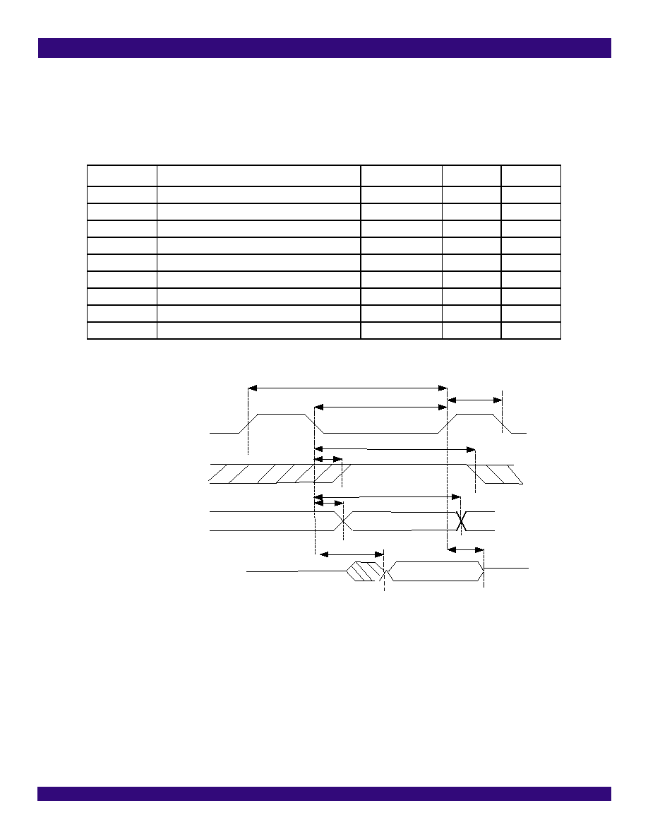
Figure 42. I/O Timing in Mode ................................................................................................................................................................................... 357
Figure 43. T1/J1 Jitter Tolerance Performance Requirement .................................................................................................................................... 362
Figure 44. E1 Jitter Tolerance Performance Requirement ........................................................................................................................................ 363
Figure 45. T1/J1 Jitter Transfer Performance Requirement (AT&T62411 / GR-253-CORE / TR-TSY-000009) ....................................................... 364
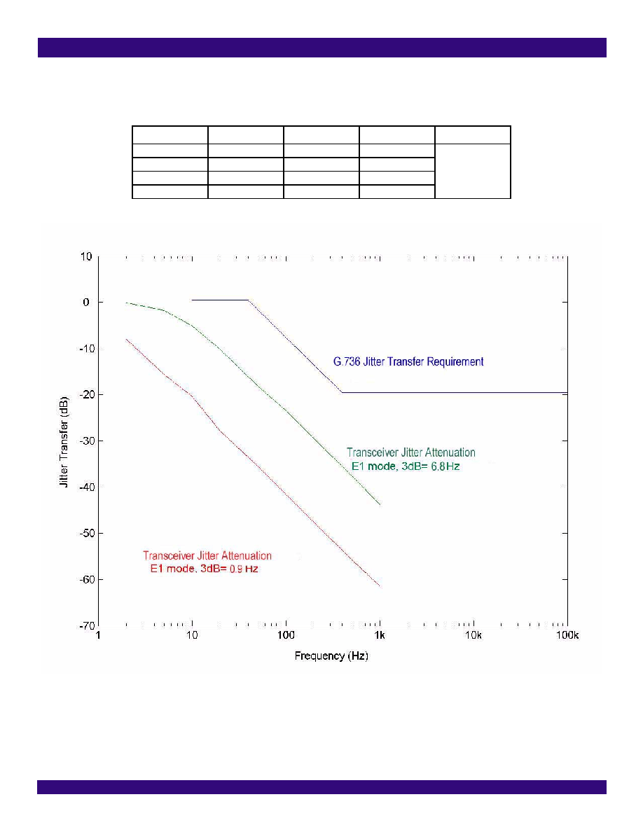
Figure 46. E1 Jitter Transfer Performance Requirement (G.736) .............................................................................................................................. 365
Figure 47. Motorola Non-Multiplexed Mode Read Cycle ........................................................................................................................................... 366
Figure 48. Motorola Non-Multiplexed Mode Write Cycle ........................................................................................................................................... 367

IDT82P2284
QUAD T1/E1/J1 LONG HAUL / SHORT HAUL TRANSCEIVER
List of Figures
ix
April 25, 2003
*Notice: The information in this document is subject to change without notice
Figure 49. Intel Non-Multiplexed Mode Read Cycle .................................................................................................................................................. 368
Figure 50. Intel Non-Multiplexed Mode Write Cycle .................................................................................................................................................. 369
Figure 51. SPI Timing Diagram ................................................................................................................................................................................. 370

1
April 25, 2003
IDT82P2284
Advance Information*
2002 Integrated Device Technology, Inc.
*Notice: The information in this document is subject to change without notice
DSC-6226/-
Quad T1/E1/J1 Long Haul /
Short Haul Transceiver
Advance Information
The IDT and the IDT logo are registered trademarks of Integrated Device Technology, Inc.
FEATURES
LINE INTERFACE
∑
Each link can be configured as T1, E1 or J1
∑
Supports T1/E1/J1 long haul/short haul line interface
∑
HPS for 1+1 protection without external relays
∑
Receive sensitivity exceeds -36 dB @ 772 Hz and -43 dB @ 1024
Hz
∑
Selectable internal line termination impedance: 100
(for T1), 75
/ 120 (for E1) and 110 (for J1)
∑
Supports AMI/B8ZS (for T1/J1) and AMI/HDB3 (for E1) line encod-
ing/decoding
∑
Provides T1/E1/J1 short haul pulse templates, long haul LBO (per
ANSI T1.403 and FCC68: 0 dB, -7.5 dB, -15 dB, -22 dB) and user-
programmable arbitrary pulse template
∑
Supports G.772 non-intrusive monitoring
∑
Supports T1.102 line monitor
∑
Transmit line short-circuit detection and protection
∑
Separate Transmit and Receive Jitter Attenuators (2 per link)
∑
Indicates the interval between the write pointer and the read pointer
of the FIFO in JA
∑
Loss of signal indication with programmable thresholds according
to ITUT-T G.775, ETS 300 233 (E1) and ANSI T1.403 (T1/J1)
∑
Supports Analog Loopback, Digital Loopback and Remote Loop-
back
∑
Each receiver and transmitter can be individually powered down
FRAMER
∑
Each link can be configured as T1, E1 or J1
∑
Frame alignment/generation for T1 (per ITU-T G.704, TA-TSY-
000278, TR-TSY-000008), E1 (per ITU-T G.704), J1 (per JT G.704)
and un-framed mode
∑
Supports T1/J1 Super Frame and Extended Super Frame, T1 Digi-
tal Multiplexer and Switch Line Carrier - 96, E1 CRC Multi-frame
and Signaling Multi-frame
∑
Signaling extraction/insertion for CAS and RBS signaling
∑
Provides programmable system interface supporting Mitel
TM
ST-
bus, AT&T
TM
CHI and MVIP bus, 8.192 Mb/s multiplexed bus and
1.544 Mb/s or 2.048 Mb/s non-multiplexed bus
∑
Three HDLC controllers per link with separate 128-byte transmit
and receive FIFOs per controller
∑
Supports Signaling System #7 (SS7)
∑
Programmable bit insertion and bit inversion on per channel/
timeslot basis
∑
Provides Bit Oriented Message (BOM) generation and detection
∑
Provides Automatic Performance Report Message (APRM) genera-
tion
∑
Detects and generates alarms (AIS, RAI)
∑
Provides performance monitor to count Bipolar Violation error,
Excess Zero error, CRC error, framing bit error, far end CRC error,
out of frame and change of framing alignment position
∑
Supports System Loopback, Payload Loopback, Digital Loopback
and Inband Loopback
∑
Detects and generates selectable PRBS and QRSS
CONTROL INTERFACE
∑
Supports Serial Peripheral Interface (SPI) microprocessor and par-
allel Intel/Motorola non-multiplexed microprocessor interface
∑
Global hardware and software reset
∑
Two general purpose I/O pins
∑
Per link power down
GENERAL
∑
Flexible reference clock (N x 1.544 MHz or N x 2.048 MHz)
(0<N<5)
∑
JTAG boundary scan
∑
3.3 V I/O with 5 V tolerant inputs
∑
Low power consumption (Typical 450 mW)
∑
3.3 V and 1.8 V power supply
∑
208-pin PBGA package
APPLICATIONS
∑
C.O, PABX, ISDN PRI
∑
Wireless Base Stations
∑
T1/E1/J1 ATM Gateways, Multiplexer
∑
T1/E1/J1 Access Networks
∑
LAN/WAN Router
∑
Digital Cross Connect
∑
SONET/SDH Add/Drop Equipment

IDT82P2284
QUAD T1/E1/J1 LONG HAUL / SHORT HAUL TRANSCEIVER
Block Diagram
2
April 25, 2003
*Notice: The information in this document is subject to change without notice
Advance Information
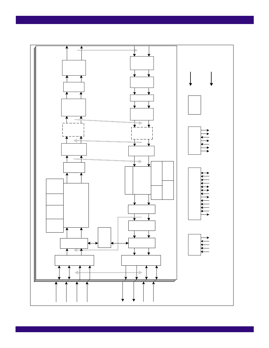
BLOCK DIAGRAM
Re
ce
i
v
e
Sys
t
em
In
te
r
f
a
c
e
RSF
S
n
RSIGn
RSD
n
MR
SCK
MRSFS
MRSIGA[1]/
MRSIG
B
[1]
MRSD
A[
1
]
/
MRSD
B[
1
]
Re
cei
v
e
Pay
l
oa
d
C
ontr
o
l
F
r
ame
Proce
sso
r
B8ZS/
HD
B3/
AMI
Dec
o
d
e
r
Re
ceive
Ji
tt
e
r
At
tenu
ator
Wavef
o
r
m
S
h
ap
er
/
Li
ne
B
u
ild
O
u
t
Data
S
lic
e
r
CL
K&Da
t
a
R
e
co
ver
y
(
D
PLL)
RT
I
P
n
RR
I
N
Gn
Tr
an
smi
t
System
In
te
r
f
a
c
e
TSI
G
n
MTSFS
TS
D
n
MTSC
K
MTSDA[
1
]
/
MTSDB[
1
]
MTSI
GA[
1
]/
MTSI
GB[
1
]
Tr
an
s
m
i
t
Pa
yl
o
a
d
Con
t
rol
F
r
am
e Ge
ne
r
a
t
o
r
Tr
an
s
m
i
t
Buff
e
r
B8
Z
S
/
HD
B3/AM
I
En
co
de
r
Tr
an
smi
t
Ji
tt
e
r
At
t
e
nu
ator
Li
n
e
Dri
v
er
TT
I
P
n
TR
I
N
G
n
O
n
e of
t
h
e Fo
ur
Li
n
k
s
(LP
1,
2
)
(L
P
4
)
G.772
Mon
i
t
o
r
C
o
n
t
ro
l In
te
rf
a
c
e
I
EEE1
14
9.1
JTAG
TCK
TMS
TDI
TDO
TRST
VDDD
I
O
/
VDDD
C /
VDD
A
R / VDD
A
T
/
VDD
AX
/
VDDAP /
VDDAB
GN
DA / GNDD
DS/RD/SCLK
CS
INT
A[9:0]
D[7:1]
No
te:
LP1
,
2 -
S
yst
e
m
Lo
op
ba
ck
LP3
- Pa
yl
o
a
d
Lo
op
ba
ck
LP4
- L
o
ca
l
D
i
gi
tal
Lo
op
bac
k 1
LP5
- R
e
mote
Lo
opb
ac
k
LP6
- L
o
ca
l
D
i
gi
tal
Lo
op
bac
k 2
LP7
- An
al
o
g
Lo
op
ba
ck
RSCKn
El
a
s
t
i
c
Stor
e
Bu
f
f
er
Re
ceive
CAS/
RBS
Buff
er
Al
a
r
m
De
t
e
ct
o
r
HD
LC
Re
cei
v
er
#1
,
#
2
, #3
Bi
t
-
Or
i
e
nted
Me
ssa
ge
Rec
e
i
v
e
r
I
n
ba
nd
Lo
op
ba
c
k
C
o
d
e
De
t
e
c
t
o
r
P
e
r
f
or
m
a
n
c
e M
o
ni
t
o
r
Ada
p
ti
ve
E
q
u
a
liz
e
r
Re
c
e
i
v
e
In
t
e
r
n
a
l
Te
rm
inati
o
n
TSFSn
TSC
K
n
Bi
t
-
Or
i
e
nted
Me
ssa
ge
Tr
an
smi
t
t
e
r
HD
LC
Tran
s
m
it
ter
#1
,
#
2
, #3
I
n
ba
nd
Lo
op
ba
c
k
C
ode
Gener
a
t
o
r
A
u
to
m
a
ti
c
Per
f
o
r
m
a
nc
e
Rep
o
rt
Mess
age
Tr
an
s
m
i
t
Interna
l
Te
r
m
in
a
t
io
n
PRBS
G
e
n
e
rator /
Detector
REFR
MPM
SPIEN
Cl
oc
k Gen
e
rator
REFA_OUT
REFB_OUT
OSCI
OSCO
CLK_SEL[2:0]
THZ
(L
P
3
)
(L
P
5
)
(LP
6)
(LP
7)
RW/WR/SDI
RESET
GPIO[1:0]
CLK_GEN_1.544
CLK_GEN_2.048
D[0]/SDO

IDT82P2284
QUAD T1/E1/J1 LONG HAUL / SHORT HAUL TRANSCEIVER
Pin Assignment
3
April 25, 2003
Advance Information
1
PIN ASSIGNMENT
Figure 1. 208-Pin PBGA (Top View)
TTIP4
TRING4
VDDAT4
VDDAR4
VDDAR3
TRING3
TTIP3
TTIP2
TRING2
VDDAR1
TRING1
TTIP1
VDDAP
RESET
REFA_
OUT
CLK_GE
N_1.544
NC
VDDAX4
GNDA
RTIP4
VDDAT3
GNDA
VDDAX3
VDDAX2
VDDAT2
GNDA
GNDA
VDDAT1
OSCI
REFB_
OUT
CLK_SEL
2
THZ
NC
NC
GNDA
RRING4
GNDA
GNDA
GNDA
GNDA
VDDAR2
GNDA
RTIP1
VDDAX1
OSCO
CLK_SEL
1
IC
REFR
NC
NC
GNDA
GNDA
RRING3
RTIP3
GNDA
RTIP2
RRING2
GNDA
RRING1
VDDAB
GPIO1
CLK_GE
N_2.048
CLK_SEL
0
IC
TSIG2/
MTSIGB1
NC
NC
NC
GPIO0
VDDDIO
VDDDIO
NC
TSIG1/
MTSIGA1
TSD2/
MTSDB1
TSD4
TSIG4
GNDD
NC
GNDD
NC
TSFS4
TSD1/
MTSDA1
TSD3
TSIG3
GNDD
GNDD
GNDD
GNDD
GNDD
NC
GNDD
VDDDIO
TSFS3
TSCK4
NC
NC
VDDDC
VDDDC
GNDD
GNDD
NC
VDDDIO
VDDDIO
NC
TSCK3
TSFS2
NC
NC
VDDDC
VDDDC
VDDDC
VDDDC
NC
GNDD
VDDDIO
NC
TSCK2
TSFS1/
MTSFS
NC
NC
VDDDC
VDDDC
VDDDC
VDDDC
GNDD
GNDD
VDDDIO
NC
TSCK1/
MTSCK
NC
NC
NC
NC
GNDD
GNDD
NC
NC
NC
NC
NC
NC
GNDD
VDDDIO
VDDDIO
NC
NC
RSIG4
RSFS3
RSFS1/
MRSFS
A2
A6
NC
D1
CS
IC
TRST
GNDD
NC
NC
VDDDIO
RSD4
RSIG2/
MRSIGB1
RSD1/
MRSDA1
RSCK3
RSCK1/
MRSCK
A3
A7
D7
D2
MPM
RW/WR
/SDI
IC
GNDD
GNDD
GNDD
VDDDIO
RSIG3
RSD2/
MRSDB1
RSFS4
RSFS2
A0
A4
A8
D6
D3
DS/RD
/SCLK
SPIEN
NC
TDI
TMS
VDDDIO
NC
RSD3
RSIG1/
MRSIGA1
RSCK4
RSCK2
A1
A5
A9
D5
D4
D0/SDO
INT
IC
TDO
TCK
NC
NC
1 2 3 4 5 6 7 8 9 10 11 12 13 14 15 16
1 2 3 4 5 6 7 8 9 10 11 12 13 14 15 16
A
B
C
D
E
F
G
H
J
K
L
M
N
P
R
T
A
B
C
D
E
F
G
H
J
K
L
M
N
P
R
T

IDT82P2284
QUAD T1/E1/J1 LONG HAUL / SHORT HAUL TRANSCEIVER
Pin Description
4
April 25, 2003
Advance Information
2
PIN DESCRIPTION
Name
Type
Pin No.
Description
Line and System Interface
RTIP[1]
RTIP[2]
RTIP[3]
RTIP[4]
RRING[1]
RRING[2]
RRING[3]
RRING[4]
Input
C11
D8
D6
B4
D11
D9
D5
C4
RTIP[1:4] / RRING[1:4]: Receive Bipolar Tip/Ring for Link 1 ~ 4
These pins are the differential line receiver inputs.
TTIP[1]
TTIP[2]
TTIP[3]
TTIP[4]
TRING[1]
TRING[2]
TRING[3]
TRING[4]
Output
A12
A8
A7
A1
A11
A9
A6
A2
TTIP[1:4] / TRING[1:4]: Transmit Bipolar Tip/Ring for Link 1 ~ 4
These pins are the differential line driver outputs and can be set to high impedance state globally or individu-
ally. A logic high on the THZ pin sets all these pins to high impedance state. When the T_HZ bit (b4, T1/J1-
023H,... / b4, E1-023H,...) * is set to `1', the TTIPn/TRINGn pins in the corresponding link are set to high
impedance state.
Besides, TTIPn/TRINGn will also be set to high impedance state by other ways (refer to Chapter 3.25 Line
Driver for details).
RSD[1] / MRSDA[1]
RSD[2] / MRSDB[1]
RSD[3]
RSD[4]
Tri-state
Output
P3
R2
T1
P1
RSD[1:4]: Receive Side System Data for Link 1 ~ 4
The processed data stream is output on these pins.
In Receive Clock Master mode, the RSDn pins are updated on the active edge of the corresponding RSCKn.
In Receive Clock Slave mode, selected by the RSLVCK bit (b4, T1/J1-010H / b4, E1-010H), the RSDn pins
are updated on the active edge of the corresponding RSCKn or all four RSDn pins are updated on the active
edge of RSCK[1].
MRSDA[1] / MRSDB[1]: Multiplexed Receive Side System Data A / B for Link 1 ~ 4
In Receive Multiplexed mode, the MRSDA[1] pin or the MRSDB[1] pin is used to output the processed data
stream. Using a byte-interleaved multiplexing scheme, the MRSDA[1]/MRSDB[1] pins output the data from
Link 1 to Link 4. The data on the MRSDA[1]/MRSDB[1] pin is updated on the active edge of the MRSCK. The
data on MRSDA[1] is the same as the data on MRSDB[1]. MRSDB[1] is for back-up purpose.
RSIG[1] / MRSIGA[1]
RSIG[2] / MRSIGB[1]
RSIG[3]
RSIG[4]
Tri-state
Output
T2
P2
R1
N3
RSIG[1:4]: Receive Side System Signaling for Link 1 ~ 4
The extracted signaling bits are output on these pins. They are located in the lower nibble (b5 ~ b8) and are
channel/timeslot-aligned with the data output on the corresponding RSDn pin.
In Receive Clock Master mode, the RSIGn pins are updated on the active edge of the corresponding RSCKn.
In Receive Clock Slave mode, selected by the RSLVCK bit (b4, T1/J1-010H / b4, E1-010H), the RSIGn pins
are updated on the active edge of the corresponding RSCKn or all four RSIGn are updated on the active edge
of RSCK[1].
MRSIGA[1] / MRSIGB[1]: Multiplexed Receive Side System Signaling A / B for Link 1 ~ 4
In Receive Multiplexed mode, the MRSIGA[1] pin or the MRSIGB[1] pin is used to output the extracted signal-
ing bits. The signaling bits are located in the lower nibble (b5 ~ b8) and are channel/timeslot-aligned with the
data output on the corresponding MRSDA[1]/MRSDB[1] pins. Using the byte-interleaved multiplexing
scheme, the MRSIGA[1]/MRSIGB[1] pins output the signaling bits from Link 1 to Link 4. The signaling bits on
the MRSIGA[1]/MRSIGB[1] pin is updated on the active edge of the MRSCK. The signaling bits on
MRSIGA[1] is the same as the signaling bits on MRSIGB[1]. MRSIGB[1] is for back-up purpose.
Note:
* The contents in the brackets indicate the position of the preceding bit and the address of the register. After the address, if the punctuation `,...' is followed, this bit is in a per-link control reg-
ister and the listed address belongs to Link 1. Users can find the omitted addresses in Chapter 5. If there is no punctuation followed the address, this bit is in a global control register.

IDT82P2284
QUAD T1/E1/J1 LONG HAUL / SHORT HAUL TRANSCEIVER
Pin Description
5
April 25, 2003
Advance Information
RSFS[1] / MRSFS
RSFS[2]
RSFS[3]
RSFS[4]
Output / Input
N5
R4
N4
R3
RSFS[1:4]: Receive Side System Frame Pulse for Link 1 ~ 4
In T1/J1 Receive Clock Master mode, RSFSn outputs the pulse to indicate each F-bit, every second F-bit in
SF frame, the first F-bit of every SF/ESF/T1 DM/SLC-96 multi-frame or the first F-bit of every second SF
multi-frame.
In T1/J1 Receive Clock Slave mode, RSFSn inputs the pulse at a rate of integer multiple of 125
µs to indicate
the start of a frame.
In E1 Receive Clock Master mode, RSFSn outputs the pulse to indicate the Basic frame, CRC Multi-frame,
Signaling Multi-frame, or both the CRC Multi-frame and Signaling Multi-frame, or the TS1 and TS16 over-
head.
In E1 Receive Clock Slave mode, RSFSn inputs the pulse at a rate of integer multiple of 125
µs to indicate
the start of a frame.
RSFSn is updated/sampled on the active edge of the corresponding RSCKn. The active polarity of RSFSn is
selected by the FSINV bit (b4, T1/J1-048H,... / b4, E1-048H,...).
MRSFS: Multiplexed Receive Side System Signaling for Link 1 ~ 4
In Receive Multiplexed mode, MRSFS inputs the pulse at a rate of integer multiple of 125
µs to indicate the
start of a frame on the multiplexed data bus. MRSFS is sampled on the active edge of MRSCK. The active
polarity of MRSFS is selected by the FSINV bit (b4, T1/J1-048H,... / b4, E1-048H,...).
RSFS[1:4]/MRSFS are Schmitt-triggered inputs/outputs with pull-up resistors.
RSCK[1] / MRSCK
RSCK[2]
RSCK[3]
RSCK[4]
Output / Input
P5
T4
P4
T3
RSCK[1:4]: Receive Side System Clock for Link 1 ~ 4
In Receive Clock Master mode, the RSCKn pins output a (gapped) 1.544 MHz (for T1/J1 mode) / 2.048 MHz
(for E1 mode) clock used to update the signal on the corresponding RSDn, RSIGn and RSFSn pins.
In Receive Clock Slave mode, the RSCKn pins input a 1.544 MHz (for T1/J1 mode only), 2.048 MHz or 4.096
MHz clock used to update the signals on the corresponding RSDn and RSIGn pins and sample the signals on
the corresponding RSFSn pins. Selected by the RSLVCK bit (b4, T1/J1-010H / b4, E1-010H), the RSCK[1]
pin can be used for all four links.
MRSCK: Multiplexed Receive Side System Clock for Link 1 ~ 4
In Receive Multiplexed mode, MRSCK inputs a 8.192 MHz or 16.384 MHz clock used to update the signals on
the corresponding MRSDA/MRSDB and MRSIGA/MRSIGB pins and sample the signal on the corresponding
MRSFS pin.
RSCK[1:4]/MRSCK are Schmitt-triggered inputs/outputs with pull-up resistors.
TSD[1] / MTSDA[1]
TSD[2] / MTSDB[1]
TSD[3]
TSD[4]
Input
G2
F2
G3
F3
TSD[1:4]: Transmit Side System Data for Link 1 ~ 4
The data stream from the system side is input on these pins.
In Transmit Clock Master mode, the TSDn pins are sampled on the active edge of the corresponding TSCKn.
In Transmit Clock Slave mode, selected by the TSLVCK bit (b1, T1/J1-010H / b1, E1-010H), the TSDn pins
are sampled on the active edge of the corresponding TSCKn or all four TSDn pins are sampled on the active
edge of TSCK[1].
MTSDA[1] / MTSDB[1]: Multiplexed Transmit Side System Data A / B for Link 1 ~ 4
In Transmit Multiplexed mode, selected by the MTSDA bit (b2, T1/J1-010H / b2, E1-010H), the MTSDA[1] pin
or the MTSDB[1] pin is used to input the data stream. Using a byte-interleaved multiplexing scheme, the
MTSDA[1]/MTSDB[1] pins input the data for Link 1 to Link 4. The data on the MTSDA[1]/MTSDB[1] pins are
sampled on the active edge of MTSCK.
TSD[1:4]/MTSDA[1]/MTSDB[1] are Schmitt-triggered inputs.
Name
Type
Pin No.
Description

IDT82P2284
QUAD T1/E1/J1 LONG HAUL / SHORT HAUL TRANSCEIVER
Pin Description
6
April 25, 2003
Advance Information
TSIG[1] / MTSIGA[1]
TSIG[2] / MTSIGB[1]
TSIG[3]
TSIG[4]
Input
F1
E1
G4
F4
TSIG[1:4]: Transmit Side System Signaling for Link 1 ~ 4
The signaling bits are input on these pins. They are located in the lower nibble (b5 ~ b8) and are channel/
timeslot-aligned with the data input on the corresponding TSDn pin.
In Transmit Clock Master mode, TSIGn is sampled on the active edge of the corresponding TSCKn.
In Transmit Clock Slave mode, selected by the TSLVCK bit (b1, T1/J1-010H / b1, E1-010H), TSIGn is sam-
pled on the active edge of the corresponding TSCKn or all four TSIGn are updated on the active edge of
TSCK[1].
MTSIGA[1] / MTSIGB[1]: Multiplexed Transmit Side System Signaling A / B for Link 1 ~ 4
In Transmit Multiplexed mode, selected by the MTSDA bit (b2, T1/J1-010H / b2, E1-010H), the MTSIGA[1] pin
or the MTSIGB[1] pin is used to input the signaling bits. The signaling bits are located in the lower nibble (b5
~ b8) and are channel/timeslot-aligned with the data input on the corresponding MTSDA[1]/MTSDB[1] pin.
Using the byte-interleaved multiplexing scheme, the MTSIGA[1]/MTSIGB[1] pins input the signaling bits for
Link 1 to Link 4. The signaling bits on the MTSIGA[1]/MTSIGB[1] pin is sampled on the active edge of
MTSCK.
TSIG[1:4]/MTSIGA[1]/MTSIGB[1] are Schmitt-triggered inputs.
TSFS[1] / MTSFS
TSFS[2]
TSFS[3]
TSFS[4]
Output / Input
K2
J2
H1
G1
TSFS[1:4]: Transmit Side System Frame Pulse for Link 1 ~ 4
In T1/J1 Transmit Clock Master mode, TSFSn outputs the pulse to indicate each F-bit or the first F-bit of every
SF/ESF/T1 DM/SLC-96 multi-frame.
In T1/J1 Transmit Clock Slave mode, TSFSn inputs the pulse to indicate each F-bit or the first F-bit of every
SF/ESF/T1 DM/SLC-96 multi-frame.
In E1 Transmit Clock Master mode, TSFSn outputs the pulse to indicate the Basic frame, CRC Multi-frame
and/or Signaling Multi-frame.
In E1 Transmit Clock Slave mode, TSFSn inputs the pulse to indicate the Basic frame, CRC Multi-frame and/
or Signaling Multi-frame.
TSFSn is updated/sampled on the active edge of the corresponding TSCKn. The active polarity of TSFSn is
selected by the FSINV bit (b1, T1/J1-042H,... / b1, E1-042H,...).
MTSFS: Multiplexed Transmit Side System Signaling for Link 1 ~ 4
In T1/J1 Transmit Multiplexed mode, MTSFS inputs the pulse to indicate each F-bit or the first F-bit of every
SF/ESF/T1 DM/SLC-96 multi-frame of one link on the multiplexed data bus.
In E1 Transmit Multiplexed mode, MTSFS inputs the pulse to indicate each Basic frame, CRC Multi-frame
and/or Signaling Multi-frame of one link on the multiplexed data bus.
MTSFS is sampled on the active edge of MTSCK. The active polarity of MTSFS is selected by the FSINV bit
(b1, T1/J1-042H,... / b1, E1-042H,...).
TSFS[1:4]/MTSFS are Schmitt-triggered inputs/outputs with pull-up resistors.
TSCK[1] / MTSCK
TSCK[2]
TSCK[3]
TSCK[4]
Output / Input
L1
K1
J1
H2
TSCK[1:4]: Transmit Side System Clock for Link 1 ~ 4
In Transmit Clock Master mode, TSCKn outputs a (gapped) 1.544 MHz (for T1/J1 mode) / 2.048 MHz (for E1
mode) clock used to sample the signal on the corresponding TSDn and TSIGn pins and update the signal on
the corresponding TSFSn pin.
In Transmit Clock Slave mode, TSCKn inputs a 1.544 MHz (for T1/J1 mode only), 2.048 MHz or 4.096 MHz
clock used to sample the signal on the corresponding TSDn, TSIGn and TSFSn pins. Selected by the
TSLVCK bit (b1, T1/J1-010H / b1, E1-010H), the TSCK[1] can be used for all four links.
MTSCK: Multiplexed Transmit Side System Clock for Link 1 ~ 4
In Transmit Multiplexed mode, MTSCK inputs a 8.192 MHz or 16.384 MHz clock used to sample the signal on
the corresponding MTSDA/MTSDB, MTSIGA/MTSIGB and MTSFS pins.
TSCK[1:4]/MTSCK are Schmitt-triggered inputs/outputs with pull-up resistors.
Clock Generator
Name
Type
Pin No.
Description

IDT82P2284
QUAD T1/E1/J1 LONG HAUL / SHORT HAUL TRANSCEIVER
Pin Description
7
April 25, 2003
Advance Information
OSCI
Input
B13
OSCI: Crystal Oscillator Input
This pin is connected to an external clock source.
The clock frequency of OSCI is defined by CLK_SEL[2:0]. The clock accuracy should be ±32 ppm and duty
cycle should be from 40% to 60%.
OSCO
Output
C13
OSCO: Crystal Oscillator Output
This pin outputs the inverted, buffered clock input from OSCI.
CLK_SEL[0]
CLK_SEL[1]
CLK_SEL[2]
Input
D15
C14
B15
CLK_SEL[2:0]: Clock Selection
These three pins select the input clock signal:
When the CLK_SEL[2] pin is low, the input clock signal is N X 1.544 MHz;
when the CLK_SEL[2] pin is high, the input clock signal is N X 2.048 MHz.
When the CLK_SEL[1:0] pins are `00', the N is 1;
when the CLK_SEL[1:0] pins are `01', the N is 2;
when the CLK_SEL[1:0] pins are `10', the N is 3;
when the CLK_SEL[1:0] pins are `11', the N is 4.
CLK_SEL[2:0] are Schmitt-trigger inputs.
CLK_GEN_1.544
Output
A16
CLK_GEN_1.544: Clock Generator 1.544 MHz Output
This pin outputs the 1.544 MHz clock signal generated by the Clock Generator.
CLK_GEN_2.048
Output
D14
CLK_GEN_2.048: Clock Generator 2.048 MHz Output
This pin outputs the 2.048 MHz clock signal generated by the Clock Generator.
REFA_OUT
Output
A15
REFA_OUT: Reference Clock Output A
This pin outputs a recovered clock from the Clock and Data Recovery function block of one of the four links.
The link is selected by the RO1[1:0] bits (b1~0, T1/J1-007H / b1~0, E1-007H).
REFB_OUT
Output
B14
REFB_OUT: Reference Clock Output B
This pin outputs a recovered clock from the Clock and Data Recovery function block of one of the four links.
The link is selected by the RO2[1:0] bits (b4~3, T1/J1-007H / b4~3, E1-007H).
Control Interface
RESET
Input
A14
RESET: Reset (Active Low)
A low pulse for more than 100 ns on this pin resets the device. All the registers are accessible 2 ms after the
reset. The RESET pin is a Schmitt-trigger input with a weak pull-up resistor.
GPIO[0]
GPIO[1]
Output / Input
E13
D13
General Purpose I/O [1:0]
These two pins can be defined as input pins or output pins by the DIR[1:0] bits (b1~0, T1/J1-006H / b1~0, E1-
006H) respectively. When the pins are input, their polarities are indicated by the LEVEL[1:0] bits (b3~2, T1/J1-
006H / b3~2, E1-006H) respectively. When the pins are ouput, their polarities are controlled by the
LEVEL[1:0] bits (b3~2, T1/J1-006H / b3~2, E1-006H) respectively.
GPIO[1:0] are Schmitt-trigger input/output with a pull-up resistor.
THZ
Input
B16
THZ: Transmit High-Z
A high level on this pin puts all the TTIPn/TRINGn pins into high impedance state.
THZ is a Schmitt-trigger input.
INT
Output
T11
INT: Interrupt (Active Low)
This is the open drain, active low interrupt output. This pin will stay low until all the active unmasked interrupt
indication bits are cleared.
REFR
Output
C16
REFR:
This pin should be connected to ground via an external 10K resistor.
CS
Input
N10
CS: Chip Select (Active Low)
This pin must be asserted low to enable the microprocessor interface. The signal must be asserted high at
least once after power up to clear the internal test modes. A transition from high to low must occur on this pin
for each Read/Write operation and can not return to high until the operation is completed.
CS is a Schmitt-trigger input.
Name
Type
Pin No.
Description

IDT82P2284
QUAD T1/E1/J1 LONG HAUL / SHORT HAUL TRANSCEIVER
Pin Description
8
April 25, 2003
Advance Information
A[0]
A[1]
A[2]
A[3]
A[4]
A[5]
A[6]
A[7]
A[8]
A[9]
Input
R5
T5
N6
P6
R6
T6
N7
P7
R7
T7
A[9:0]: Address Bus
In parallel mode, the signals on these pins select the register for the microprocessor to access.
In SPI mode, these pins should be connected to ground.
A[9:0] are Schmitt-trigger inputs.
D[0] / SDO
D[1]
D[2]
D[3]
D[4]
D[5]
D[6]
D[7]
Output / Input
T10
N9
P9
R9
T9
T8
R8
P8
D[7:0]: Bi-directional Data Bus
In parallel mode, the signals on these pins are the data for Read / Write operation.
In SPI mode, the D[7:1] pins should be connected to the ground through a 10 K resistor.
D[7:0] are Schmitt-trigger inputs/outputs.
SDO: Serial Data Output
In SPI mode, the data is serially output on this pin.
MPM
Input
P11
MPM: Micro Controller Mode
In parallel mode, set this pin low for Motorola mode or high for Intel mode.
In SPI mode, set this pin to a fixed level (high or low). This pin is useless in SPI mode.
MPM is a Schmitt-trigger input.
RW / WR / SDI
Input
P10
RW: Read / Write Select
In parallel Motorola mode, this pin is active high for read operation and active low for write operation.
WR: Write Strobe (Active Low)
In parallel Intel mode, this pin is active low for write operation.
SDI: Serial Data Input
In SPI mode, the address/control and/or data are serially input on this pin.
RW / WR / SDI is a Schmitt-trigger input.
DS / RD / SCLK
Input
R10
DS: Data Strobe (Active Low)
In parallel Motorola mode, this pin is active low.
RD: Read Strobe (Active Low)
In parallel Intel mode, this pin is active low for read operation.
SCLK: Serial Clock
In SPI mode, this pin inputs the timing for the SDO and SDI pins. The signal on the SDO pin is updated on the
falling edge of SCLK, while the signal on the SDI pin is sampled on the rising edge of SCLK.
DS / RD / SCLK is a Schmitt-trigger input.
SPIEN
Input
R11
SPIEN: Serial Microprocessor Interface Enable
When this pin is low, the microprocessor interface is in parallel mode.
When this pin is high, the microprocessor interface is in SPI mode.
SPIEN is a Schmitt-trigger input.
JTAG (per IEEE 1149.1)
TRST
Input
N12
TRST: Test Reset (Active Low)
A low signal on this pin resets the JTAG test port. This pin is a Schmitt-triggered input with an internal pull-up
resistor. It must be connected to the RESET pin or ground when JTAG is not used.
Name
Type
Pin No.
Description

IDT82P2284
QUAD T1/E1/J1 LONG HAUL / SHORT HAUL TRANSCEIVER
Pin Description
9
April 25, 2003
Advance Information
TMS
Input
R14
TMS: Test Mode Select
The signal on this pin controls the JTAG test performance and is sampled on the rising edge of TCK. This pin
is a Schmitt-triggered input with an internal pull-up resistor.
TCK
Input
T14
TCK: Test Clock
The clock for the JTAG test is input on this pin. TDI and TMS are sampled on the rising edge of TCK and TDO
is clocked out of the device on the falling edge of TCK. This pin is a Schmitt-triggered input with an internal
pull-up resistor.
TDI
Input
R13
TDI: Test Input
The test data is sampled at this pin on the rising edge of TCK. This pin is a Schmitt-triggered input with an
internal pull-up resistor.
TDO
Tri-State
T13
TDO: Test Output
The test data are output on this pin. It is updated on the falling edge of TCK. This pin is tri-stated except dur-
ing the process of data scanning.
Power & Ground
VDDDIO
Power
E14
E15
G16
H14
H15
J15
K15
M15
M16
N16
P16
R15
VDDDIO: 3.3 V I/O Power Supply
VDDDC
Power
H7
H8
J7
J8
J9
J10
K7
K8
K9
K10
VDDDC: 1.8 V Digital Core Power Supply
VDDAR[1]
VDDAR[2]
VDDAR[3]
VDDAR[4]
Power
A10
C9
A5
A4
VDDAR[8:1]: 3.3 V Power Supply for Receiver
VDDAT[1]
VDDAT[2]
VDDAT[3]
VDDAT[4]
Power
B12
B9
B5
A3
VDDAT[8:1]: 3.3 V Power Supply for Transmitter
VDDAX[1]
VDDAX[2]
VDDAX[3]
VDDAX[4]
Power
C12
B8
B7
B2
VDDAX[8:1]: 3.3 V Power Supply for Transmit Driver
VDDAP
Power
A13
VDDAP: 3.3 V Power Analog PLL
VDDAB
Power
D12
VDDAB: 3.3 V Power Analog Bias
Name
Type
Pin No.
Description

IDT82P2284
QUAD T1/E1/J1 LONG HAUL / SHORT HAUL TRANSCEIVER
Pin Description
10
April 25, 2003
Advance Information
GNDA
Ground
B3
B6
B10
B11
C3
C5
C6
C7
C8
C10
D3
D4
D7
D10
GNDA: Analog Ground
GNDD
Ground
F13
F15
G7
G8
G9
G10
G13
G15
H9
H10
J14
K13
K14
L14
L15
M14
N13
P13
P14
P15
GNDD: Digital Ground
TEST
IC
-
C15
D16
N11
P12
T12
IC: Internal Connected
Thess pins are for IDT use only and should be connected to ground.
Others
Name
Type
Pin No.
Description

IDT82P2284
QUAD T1/E1/J1 LONG HAUL / SHORT HAUL TRANSCEIVER
Pin Description
11
April 25, 2003
Advance Information
NC
-
B1, C1, C2, D1,
D2, E2, E3, E4,
E16, F14, F16,
G14, H3, H4,
H13, H16, J3,
J4, J13, J16,
K3, K4, K16,
L2, L3, L4, L13,
L16, M1, M2,
M3, M4, M13,
N1, N2, N8,
N14, N15, R12,
R16, T15, T16
NC: Not Connected
Name
Type
Pin No.
Description

IDT82P2284
QUAD T1/E1/J1 LONG HAUL / SHORT HAUL TRANSCEIVER
Functional Description
12
April 25, 2003
Advance Information
3
FUNCTIONAL DESCRIPTION
The IDT82P2284 is a highly featured single device solution for T1/
E1/J1 trunks. Each link of the IDT82P2284 can be independently config-
ured. The configuration is performed through a SPI or parallel micropro-
cessor interface.
LINE INTERFACE - RECEIVE PATH
In the receive path, the signals from the line side are coupled into
the RTIPn and RRINGn pins and pass through an Impedance Termina-
tor. An Adaptive Equalizer is provided to increase the sensitivity for small
signals. Clock and data are recovered from the digital pulses output from
the slicer. After passing through the Receive Jitter Attenuator (can be
enabled or disabled), the recovered data is decoded using B8ZS (for T1/
J1) / HDB3 (for E1) or AMI line code rules and clocked into the Frame
Processor. Loss of signal, line code violations and excessive zero are
detected.
FRAMER - RECEIVE PATH
In T1/J1 Mode, the recovered data and clock of each link can be
configured in Super Frame (SF), Extended Super Frame (ESF), T1 Digi-
tal Multiplexer (DM) or Switch Line Carrier - 96 (SLC-96) formats. (The
T1 DM and SLC-96 formats only exist in T1 mode). The framing can also
be bypassed (unframed mode). The Framer detects and indicates the
out of SF/ESF/DM/SLC-96 synchronization event, the Yellow, Red and
AIS alarms. The Framer also detects the presence of inband loopback
codes and bit-oriented messages. Frame Alignment Signal errors, CRC-
6 errors, out of SF/ESF/T1 DM/SLC-96 events and Frame Alignment
position changes are counted. Up to three HDLC links (in ESF and T1
DM format) or two HDLC links (in SF and SLC-96 format) are provided
to extract the HDLC message on the DL bit (in ESF format) / D bit in
CH24 (in T1 DM format) or any arbitrary position. In the T1/J1 receive
path, signaling debounce, signaling freeze, idle code substitution, digital
milliwatt code insertion, idle code insertion, data inversion and pattern
generation or detection are supported on a per-channel basis. An Elastic
Store Buffer that supports controlled slip and adaptation to backplane
timing may be enabled. In the Receive System Interface, various operat-
ing modes can be selected to output signals to the system.
In E1 Mode, the recovered data and clock of each link can be con-
figured to frame to Basic Frame, CRC Multi-Frame and Signaling Multi-
Frame. The framing can be bypassed (unframed mode). The Framer
detects and indicates the following event: out of Basic Frame Sync, out
of CRC Multi-Frame, out of Signaling Multi-Frame, Remote Alarm Indi-
cation signal and Remote Signaling Multi-Frame Alarm Indication signal.
The Framer also monitors Red and AIS alarms. Basic Frame Alignment
Signal errors, Far End Block Errors (FEBE) and CRC errors are
counted. Up to three HDLC links are provided to extract the HDLC mes-
sage on TS16, the Sa National bits or any arbitrary timeslot. In the E1
receive path, signaling debounce, signaling freezing, idle code substitu-
tion, digital milliwatt code insertion, trunk conditioning, data inversion
and pattern generation or detection are also supported on a per-timeslot
basis. An Elastic Store Buffer that supports slip buffering and adaptation
to backplane timing may be enabled. In the Receive System Interface,
various operating modes can be selected to output signals to the sys-
tem.
SYSTEM INTERFACE
On the system side, if the device is in T1/J1 mode, the data stream
of 1.544 Mbit/s can be converted to/from the data stream of 2.048 Mbit/s
by software configuration. In addition, the four links can be grouped into
one set. The set can be multiplexed to or de-multiplexed from one of the
two 8.192 Mbit/s buses. If the device is in E1 mode, the four links can be
multiplexed to or de-multiplexed from one of the two 8.192 Mbit/s buses.
FRAMER - TRANSMIT PATH
In the transmit path, the Transmit System Interface inputs the sig-
nals with various operating modes. In T1/J1 mode, the signals can be
processed by a Transmit Payload Control to execute the signaling inser-
tion, idle code substitution, data insertion, data inversion and test pattern
generation or detection on a per-channel basis. The transmit path of
each transceiver can be configured to generate SF, ESF, T1 DM or SLC-
96. The framer can also be disabled (unframed mode). The Framer can
transmit Yellow alarm and AIS alarm. Inband loopback codes and bit ori-
ented message can be transmitted. Up to three HDLC links (in ESF and
T1 DM format) or two HDLC links (in SF and SLC-96 format) are pro-
vided to insert the HDLC message on the DL bit (in ESF format) / D bit in
CH24 (in T1 DM format) or any arbitrary position. After passing through
a Transmit Buffer, the processed data and clock are input to the
Encoder.
In E1 mode, the signals can be processed by a Transmit Payload
Control to execute the signaling insertion, idle code substitution, data
insertion, data inversion and test pattern generation or detection on a
per-timeslot basis. The transmit path of each transceiver can be config-
ured to generate Basic Frame, CRC Multi-Frame and Signaling Multi-
Frame. The framer can be disabled (unframed mode). The Framer can
transmit Remote Alarm Indication signal, the Remote Signaling Multi-
Frame Alarm Indication signal, AIS alarm and FEBE. Three HDLC links
are provided to insert the HDLC message on TS16, the Sa National bits
or any arbitrary timeslot. The processed data and clock are input to the
Encoder.
LINE INTERFACE - TRANSMIT PATH
The data is encoded using AMI or B8ZS (for T1/J1) and HDB3 (for
E1) line code rules. The Transmit Jitter Attenuator, if enabled, is pro-
vided with a FIFO in the transmit data path. A de-jittered clock is gener-
ated by an integrated digital phase-locked loop and is used to read data
from the FIFO. The shapes of the pulses are user programmable to
ensure that the T1/E1/J1 pulse template is met after the signal passing
through different cable lengths and types. Bipolar violation can be
inserted for diagnostic purposes if AMI line code rule is enabled. The
signal is transmitted on the TTIPn and TRINGn pins through an Imped-
ance Terminator.

IDT82P2284
QUAD T1/E1/J1 LONG HAUL / SHORT HAUL TRANSCEIVER
Functional Description
13
April 25, 2003
Advance Information
TEST AND DIAGNOSES
To facilitate the testing and diagnostic functions, Analog Loopback,
Remote Digital Loopback, Remote Loopback, Local Digital Loopback,
Payload Loopback and System Loopback are also integrated in the
IDT82P2284. A programmable pseudo random bit sequence can be
generated in receive/transmit direction and detected in the opposite
direction for testing purpose.
The G.772 Non-intrusive monitoring and JTAG are also supported
by the IDT82P2284.

IDT82P2284
QUAD T1/E1/J1 LONG HAUL / SHORT HAUL TRANSCEIVER
Functional Description
14
April 25, 2003
Advance Information
3.1
T1 / E1 / J1 MODE SELECTION
Each link in the IDT82P2284 can be configured as a duplex T1
transceiver, or a duplex E1 transceiver, or a duplex J1 transceiver. When
it is in T1 mode, Super Frame (SF), Extended Super Frame (ESF), T1
Digital Multiplexer (T1 DM) and Switch Line Carrier - 96 (SLC-96) fram-
ing formats can be selected. When it is in J1 mode, Super Frame (SF)
and Extended Super Frame (ESF) formats can be selected. All the
selections are made by the TEMODE bit, the T1/J1 bit and the FM[1:0]
bits as shown in Table 1.
Table 1: Operating Mode Selection
TEMODE T1/J1 FM[1:0]
Operating Mode
1
0
0 0
T1 mode SF format
0 1
T1 mode ESF format
1 0
T1 mode T1 DM format
1 1
T1 mode SLC-96 format
1
0 0
J1 mode SF format
0 1
J1 mode ESF format
0
X
X
E1 mode
Table 2: Related Bit / Register In Chapter 3.1
Bit
Register
Address (Hex)
TEMODE
T1/J1 Or E1 Mode
020, 120, 220, 320
T1/J1
FM[1:0]

IDT82P2284
QUAD T1/E1/J1 LONG HAUL / SHORT HAUL TRANSCEIVER
Functional Description
15
April 25, 2003
Advance Information
3.2
RECEIVER IMPEDANCE MATCHING
The receiver impedance matching can be realized by using internal
impedance matching circuit or external impedance matching circuit.
When the R_TERM[2] bit is `0', the internal impedance matching
circuit is enabled. 100
, 110 , 75 or 120 internal impedance
matching circuit can be selected by the R_TERM[1:0] bits.
When the R_TERM[2] bit is `1', the internal impedance matching
circuit is disabled, and different external resistors should be used to real-
ize different impedance matching.
Figure 2 shows the appropriate components to connect with the
cable for one link. Table 3 lists the recommended impedance matching
value for the receiver.
Figure 2. Receive / Transmit Line Circuit
In short haul applications, after the data stream passes through the
receive internal impedance circuitry, the non-intrusive monitoring can be
performed between two devices. The monitored link of one device is in
normal operation, and the monitoring link of the other device taps the
monitored one through a high impedance bridging circuit (refer to
Figure 3 and Figure 4). Because of the high resistance bridging circuit,
the signal arriving at the RTIPn/RRINGn of the monitoring link is dramat-
ically attenuated. To compensate this attenuation, the Monitor Gain can
be used to boost the signal by 22 dB, 26 dB and 32 dB selected by the
MG[1:0] bits. For normal operation, the Monitor Gain should be set to 0
dB, i.e. the Monitor Gain of the monitored link should be 0 dB.
Table 3: Impedance Matching Value For The Receiver
Cable
Configuration
Internal Termination
External Termination
R_TERM[2:0]
R
R
R_TERM[2:0]
R
R
75
(E1)
0 0 0
120
1 X X
75
120
(E1)
0 0 1
120
100
(T1)
0 1 0
100
110
(J1)
0 1 1
110
A
B
∑
∑
∑ ∑
R
X
Line
R
R
∑
∑
T
X
Line
R
T
R
T
RTIP
RRING
TRING
TTIP
I
D
T82
P2284
(
o
ne of
t
he f
o
u
r
i
dent
i
c
al
l
i
n
ks)
VDDAX
VDDAX
D4
D3
D2
D1
1:1
2:1
∑
∑
D6
D5
∑
D8
D7
∑
Cp
VDDAR
VDDAR
Note: 1. Common decoupling capacitor
2. Cp 0-560 (pF)
3. D1 - D8, Motorola - MBR0540T1; International Rectifier - 11DQ04 or 10BQ060
∑
0.1
µF
GNDA
VDDAX
68
µF
1
3.3 V
∑
0.1
µF
GNDA
VDDAR
68
µF
3.3 V
1

IDT82P2284
QUAD T1/E1/J1 LONG HAUL / SHORT HAUL TRANSCEIVER
Functional Description
16
April 25, 2003
Advance Information
Figure 3. Monitoring Receive Path
Figure 4. Monitoring Transmit Path
RTIPn
RRINGn
RTIPn
RRINGn
Monitored Link
Monitoring Link
DSX cross connect point
R
Monitor Gain
= 0 dB
Monitor Gain
=22/26/32 dB
TTIPn
TRINGn
RTIPn
RRINGn
Monitored Link
Monitoring Link
DSX cross connect point
R
Monitor Gain
=22/26/32 dB
Table 4: Related Bit / Register In Chapter 3.2
Bit
Register
Address (Hex)
R_TERM[2:0]
Transmit And Receive Termination Configuration
032, 132, 232, 332
MG[1:0]
Receive Configuration 2
02A, 12A, 22A, 32A

IDT82P2284
QUAD T1/E1/J1 LONG HAUL / SHORT HAUL TRANSCEIVER
Functional Description
17
April 25, 2003
Advance Information
3.3
ADAPTIVE EQUALIZER
The Adaptive Equalizer can remove most of the signal distortion
due to intersymbol interference caused by cable attenuation and distor-
tion. Usually, the Adaptive Equalizer is off in short haul applications and
is on in long haul applications, which is configured by the EQ_ON bit.
The peak detector keeps on measuring the peak value of the
incoming signals during a selectable observation period. The observa-
tion period is selected by the UPDW[1:0] bits. A shorter observation
period allows quicker response to pulse amplitude variation, while a
longer observation period can minimize the possible overshoots.
Based on the observed peak value for a period, the equalizer will
be adjusted to achieve a normalized signal. The LATT[4:0] bits indicate
the signal attenuation introduced by the cable in approximately 2 dB per
step.
In short haul application, the receive sensitivity is -10 dB in both T1/
J1 and E1 modes. In long haul application, the receive sensitivity is -36
dB in T1/J1 mode or -43 dB in E1 mode.
3.4
DATA SLICER
The Data Slicer is used to generate a standard amplitude mark or a
space according to the amplitude of the input signals. The criteria of
mark or space generation are based on a selected ratio of the incoming
signal amplitude against the peak value detected during the observation
period. This ratio is selected by the SLICE[1:0] bits. The output of the
Data Slicer is forwarded to the Clock and Data Recovery unit.
3.5
CLOCK AND DATA RECOVERY
The Clock and Data Recovery is used to recover the clock signal
from the received data. It is accomplished by Digital Phase Locked Loop
(DPLL). The recovered clock tracks the jitter in the data output from the
Data Slicer and keeps the phase relationship between data and clock
during the absence of the incoming pulse.
Table 5: Related Bit / Register In Chapter 3.3 & Chapter 3.4
Bit
Register
Address (Hex)
EQ_ON
Receive Configuration 1
029, 129, 229, 329
UPDW[1:0]
Receive Configuration 2
02A, 12A, 22A, 32A
SLICE[1:0]
LATT[4:0]
Line Status Register 1
037, 137, 237, 337

IDT82P2284
QUAD T1/E1/J1 LONG HAUL / SHORT HAUL TRANSCEIVER
Functional Description
18
April 25, 2003
Advance Information
3.6
RECEIVE JITTER ATTENUATOR
The Receive Jitter Attenuator of each link can be chosen to be
used or not. This selection is made by the RJA_E bit.
The Jitter Attenuator consists of a FIFO and a DPLL, as shown in
Figure 5.
Figure 5. Jitter Attenuator
The FIFO is used as a pool to buffer the jittered input data, then the
data is clocked out of the FIFO by a de-jittered clock. The depth of the
FIFO can be 32 bits, 64 bits or 128 bits, as selected by the RJA_DP[1:0]
bits. Accordingly, the constant delay produced by the Jitter Attenuator is
16 bits, 32 bits or 64 bits. The 128-bit FIFO is used when large jitter tol-
erance is expected, while the 32-bit FIFO is used in delay sensitive
applications.
The DPLL is used to generate a de-jittered clock to clock out the
data stored in the FIFO. The DPLL can only attenuate the incoming jitter
whose frequency is above Corner Frequency (CF). The jitter whose fre-
quency is lower than the CF passes through the DPLL without any atten-
uation. In T1/J1 applications, the CF of the DPLL can be 5 Hz or 1.26
Hz, as selected by the RJA_BW bit. In E1 applications, the CF of the
DPLL can be 6.77 Hz or 0.87 Hz, as selected by the RJA_BW bit. The
lower the CF is, the longer time is needed to achieve synchronization.
If the incoming data moves faster than the outgoing data, the FIFO
will overflow. If the incoming data moves slower than the outgoing data,
the FIFO will underflow. The overflow or underflow is captured by the
RJA_IS bit. When the RJA_IS bit is `1', an interrupt will be reported on
the INT pin if enabled by the RJA_IE bit.
To avoid overflow or underflow, the JA-Limit function can be
enabled by setting the RJA_LIMT bit. When the JA-Limit function is
enabled, the speed of the outgoing data will be adjusted automatically if
the FIFO is close to its full or emptiness. The criteria of speed adjust-
ment start are listed in Table 6. Though the JA-Limit function can reduce
the possibility of FIFO overflow and underflow, the quality of jitter attenu-
ation is deteriorated.
Selected by the RJITT_TEST bit, the real time interval between the
read and write pointer of the FIFO or the peak-peak interval between the
read and write pointer of the FIFO can be indicated in the RJITT[6:0]
bits. When the RJITT_TEST bit is `0', the current interval between the
read and write pointer of the FIFO will be written into the RJITT[6:0] bits.
When the RJITT_TEST bit is `1', the current interval will be compared
with the old one in the RJITT[6:0] bits and the larger one will be indi-
cated by the RJITT[6:0] bits.
The performance of Receive Jitter Attenuator meets the ITU-T
I.431, G.703, G.736 - 739, G.823, G.824, ETSI 300011, ETSI TBR 12/
13, AT&T TR62411, TR43802, TR-TSY 009, TR-TSY 253, TR-TRY 499
standards. Refer to Chapter 7.9 Jitter Tolerance and Chapter 7.10 Jitter
Transfer for details.
Table 6: Criteria Of Speed Adjustment Start
FIFO Depth
Criteria Of Speed Adjustment Start
32 bits
2-bit close to full or empty
64 bits
3-bit close to full or empty
128 bits
4-bit close to full or empty
FIFO
32/64/128
DPLL
Jittered Data
De-jittered Data
Jittered Clock
De-jittered Clock
write
pointer
read
pointer
Table 7: Related Bit / Register In Chapter 3.6
Bit
Register
Address (Hex)
RJA_E
Receive Jitter Attenuation Configuration 027, 127, 227, 327
RJA_DP[1:0]
RJA_BW
RJA_LIMT
RJITT_TEST
RJA_IS
Interrupt Status 1
03B, 13B, 23B, 33B
RJA_IE
Interrupt Enable Control 1
034, 134, 234, 334
RJITT[6:0]
Receive Jitter Measure Value Indication 039, 139, 239, 339

IDT82P2284
QUAD T1/E1/J1 LONG HAUL / SHORT HAUL TRANSCEIVER
Functional Description
19
April 25, 2003
Advance Information
3.7
DECODER
3.7.1
LINE CODE RULE
3.7.1.1
T1 / J1 Mode
In T1/J1 mode, the AMI and B8ZS line code rules are provided. The
selection is made by the R_MD bit.
3.7.1.2
E1 Mode
In E1 mode, the AMI and HDB3 line code rules are provided. The
selection is made by the R_MD bit.
3.7.2
DECODE ERROR DETECTION
3.7.2.1
T1 / J1 Mode
The decode errors can be divided into three types in T1/J1 mode:
1. Bipolar Violation (BPV) Error: When AMI line code rule is used,
the BPV error will be detected if two consecutive pulses are received
with the same polarity (refer to Figure 6). The event of the Bipolar Viola-
tion (BPV) Error is forwarded to the Performance Monitor.
2. B8ZS Code Violation (CV) Error: When B8ZS line code rule is
used, a CV error is detected when the received code does not match the
standard B8ZS line code pattern (expect the Excessive Zero error).
3. Excessive Zero (EXZ) Error: EXZ error can be detected in both
AMI and B8ZS line code rules. There are two standards defining the
EXZ error: ANSI and FCC. The EXZ_DEF bit chooses a standard for the
corresponding link to judge the EXZ error. Table 8 shows the definition of
EXZ. To count the event of the Excessive Zero (EXZ) Error, the
EXZ_ERR[1:0] bits should be set to `01'. The Excessive Zero (EXZ)
Error is counted in an internal 16-bit EXZ counter. The content in the
EXZ counter is transferred to the EXZ Error Counter L-Byte & H-Byte
registers in two ways:
a. When the CNT_MD bit is `0', the Manual-Report mode is
selected. The EXZ counter transfers its content to the EXZ Error
Counter L-Byte & H-Byte registers when there is a transition from `0' to
`1' on the CNT_TRF bit;
b. When the CNT_MD bit is `1', the Auto-Report mode is selected.
The EXZ counter transfers its content to the EXZ Error Counter L-Byte &
H-Byte registers every one second automatically.
After the content in the counter is transferred to the EXZ Error
Counter L-Byte & H-Byte registers, the counter will be cleared to `0' and
start a new round counting automatically. No error event is lost during
data transferring.
The overflow of the counter is reflected by the CNTOV_IS bit, and
can trigger an interrupt if the corresponding CNT_IE bit is set.
When the Bipolar Violation (BPV) Error or the B8ZS Code Violation
(CV) Error is detected, it will be indicated by the CV_IS bit. When the
Excessive Zero (EXZ) Error is detected, it will be indicated by the
EXZ_IS bit. When the CV_IS bit or the EXZ_IS bit is `1', an interrupt will
be reported by the INT pin if enabled by the corresponding CV_IE bit or
the EXZ_IE bit.
3.7.2.2
E1 Mode
The decode errors can be divided into three types in E1 mode:
1. Bipolar Violation (BPV) Error: When AMI line code rule is used,
the BPV error will be detected if two consecutive pulses are received
with the same polarity (refer to Figure 6). The event of the Bipolar Viola-
tion (BPV) Error is forwarded to the Performance Monitor.
2. HDB3 Code Violation (CV) Error: When HDB3 line code rule is
used, a CV error is detected if two consecutive BPV errors are detected,
and the pulses that have the same polarity as the previous pulse are not
the HDB3 zero substitution pulsed (refer to Figure 8).
3. Excessive Zero (EXZ) Error: EXZ error can be detected in both
AMI and HDB3 line code rules. There are two standards defining the
EXZ error: ANSI and FCC. The EXZ_DEF bit chooses a standard for the
corresponding link to judge the EXZ error. Table 8 shows the definition of
EXZ. To count the event of the Excessive Zero (EXZ) Error, the
EXZ_ERR[1:0] bits should be set to `01'. The Excessive Zero (EXZ)
Error is counted in an internal 16-bit EXZ counter. The content in the
EXZ counter is transferred to the EXZ Error Counter L-Byte & H-Byte
registers in two ways:
a. When the CNT_MD bit is `0', the Manual-Report mode is
selected. The EXZ counter transfers its content to the EXZ Error
Counter L-Byte & H-Byte registers when there is a transition from `0' to
`1' on the CNT_TRF bit;
b. When the CNT_MD bit is `1', the Auto-Report mode is selected.
The EXZ counter transfers its content to the EXZ Error Counter L-Byte &
H-Byte registers every one second automatically.
After the content in the counter is transferred to the EXZ Error
Counter L-Byte & H-Byte registers, the counter will be cleared to `0' and
start a new round counting automatically. No error event is lost during
data transferring.
The overflow of the counter is reflected by the CNTOV_IS bit, and
can trigger an interrupt if the corresponding CNT_IE bit is set.
When the Bipolar Violation (BPV) Error or the HDB3 Code Violation
(CV) Error is detected, it will be indicated by the CV_IS bit. When the
Excessive Zero (EXZ) Error is detected, it will be indicated by the
EXZ_IS bit. When the CV_IS bit or the EXZ_IS bit is `1', an interrupt will
be reported by the INT pin if enabled by the corresponding CV_IE bit or
the EXZ_IE bit.
Table 8: Excessive Zero Error Definition
ANSI
FCC
AMI
More than 15 consecutive 0s are
detected.
More than 80 consecutive 0s are
detected.
B8ZS
More than 8 consecutive 0s are
detected (refer to Figure 7).
More than 8 consecutive 0s are
detected (refer to Figure 7).
HDB3
More than 3 consecutive 0s are
detected (refer to Figure 8).
More than 3 consecutive 0s are
detected (refer to Figure 8).

IDT82P2284
QUAD T1/E1/J1 LONG HAUL / SHORT HAUL TRANSCEIVER
Functional Description
20
April 25, 2003
Advance Information
Figure 6. AMI Bipolar Violation Error
Figure 7. B8ZS Excessive Zero Error
Figure 8. HDB3 Code Violation & Excessive Zero Error
3.7.3
LOS DETECTION
The Loss of Signal (LOS) Detector monitors the amplitude and den-
sity of the received signal. When the received signal is below an ampli-
tude for continuous intervals, the LOS is detected. When the received
signal is above the amplitude and the density of marks meets the
requirement, the LOS is cleared.
The different criteria for LOS Declaring/Clearing are illustrated in
Table 9 and Table 10. In T1/J1 mode, the LOS detection supports ANSI
T1.231 and I.431. In E1 mode, the LOS detection supports ITU-T G.775
and I.431. The criteria are selected by the LAC bit.
When the LOS is detected, it will be indicated by the LOS_S bit.
Selected by the LOS_IES bit, a transition from '0' to '1' on the LOS_S bit
or any transition (from `0' to `1' or from `1' to `0') on the LOS_S bit will set
the LOS_IS bit to `1'. When the LOS_IS bit is `1', an interrupt will be
reported by the INT pin if enabled by the LOS_IE bit.
During LOS, if the RAISE bit is set to `1', all 'One's will be inserted
to the received data stream.
Bipolar violation
clock
RTIPn
RRINGn
1
2
3
4
5
V
6
7
Excessive zero
clock
RTIPn
RRINGn
8 consecutive
zeros
1
2
3
5
4
6
7
8
9
Excessive zero
clock
RTIPn
RRINGn
Code violation
4 consecutive
zeros
1
2
3
4
V
V
5
6

IDT82P2284
QUAD T1/E1/J1 LONG HAUL / SHORT HAUL TRANSCEIVER
Functional Description
21
April 25, 2003
Advance Information
Table 9: LOS Condition In T1/J1 Mode
Loss of Signal in T1/J1 Mode
Short Haul Application
Long Haul Application
ANSI T1.231
I.431
ANSI T1.231
I.431
LOS
Detected
Amplitude
below 800 mVpp
below 800 mVpp
below Q dB *
below Q dB *
Continuous Intervals 175 bits
1544 bits
175 bits
1544 bits
LOS
Cleared
Amplitude
above 1 Vpp
above 1 Vpp
above Q + 4 dB *
above Q + 4 dB *
Mark Density
12.5% (16 marks in a hopping
128-bit window **) with less
than 100 continuous zeros
12.5% (16 marks in a hopping
128-bit window **) with less
than 100 continuous zeros
12.5% (16 marks in a hopping
128-bit window **) with less
than 100 continuous zeros
12.5% (16 marks in a hopping
128-bit window **) with less
than 100 continuous zeros
Note:
* The Q dB is set in the LOS[4:0] bits.
** A hopping 128-bit window means this: An entire 128 bits is taken from the data stream and is checked. If the criteria are not met, all the 128 bits are thrown and another 128 bits are
caught for checking.
Table 10: LOS Condition In E1 Mode
Loss of Signal in E1 Mode
Short Haul Application
Long Haul Application
G.775
I.431
G.775
I.431
LOS
Detected
Amplitude
below 800 mVpp
below 800 mVpp
below Q dB *
below Q dB *
Continuous Intervals 32 bits
2048 bits
32 bits
2048 bits
LOS
Cleared
Amplitude
above 1 Vpp
above 1 Vpp
above Q + 4 dB *
above Q + 4 dB *
Mark Density
12.5% (4 marks in a hopping
32-bit window **) with less than
16 continuous zeros
12.5% (4 marks in a hopping
32-bit window **) with less than
16 continuous zeros
12.5% (4 marks in a hopping
32-bit window **) with less than
16 continuous zeros
12.5% (4 marks in a hopping
32-bit window **) with less than
16 continuous zeros
Note:
* The Q dB is set in the LOS[4:0] bits.
** A hopping 32-bit window means this: An entire 32 bits is taken from the data stream and is checked. If the criteria are not met, all the 32 bits are thrown and another 32 bits are caught
for checking.

IDT82P2284
QUAD T1/E1/J1 LONG HAUL / SHORT HAUL TRANSCEIVER
Functional Description
22
April 25, 2003
Advance Information
Table 11: Related Bit / Register In Chapter 3.7
Bit
Register
Address (Hex)
R_MD
Receive Configuration 0
028, 128, 228, 328
EXZ_ERR
Maintenance Function Control 2
031, 131, 231, 331
EXZ_DEF
CNT_MD
CNT_TRF
CNTL[7:0]
EXZ Error Counter L-Byte
03D, 13D, 23D, 33D
CNTH[7:0]
EXZ Error Counter H-Byte
03C, 13C, 23C, 33C
CV_IS
Interrupt Status 1
03B, 13B, 23B, 33B
EXZ_IS
CNTOV_IS
CV_IE
Interrupt Enable Control 1
034, 134, 234, 334
EXZ_IE
CNT_IE
LAC
Maintenance Function Control 1
02C, 12C, 22C, 32C
RAISE
LOS_S
Line Status Register 0
036, 136, 236, 336
LOS_IES
Interrupt Trigger Edges Select
035, 135, 235, 335
LOS_IS
Interrupt Status 0
03A, 13A, 23A, 33A
LOS_IE
Interrupt Enable Control 0
033, 133, 233, 333
LOS[4:0]
Receive Configuration 1
029, 129, 229, 329

IDT82P2284
QUAD T1/E1/J1 LONG HAUL / SHORT HAUL TRANSCEIVER
Functional Description
23
April 25, 2003
Advance Information
3.8
FRAME PROCESSOR
3.8.1
T1/J1 MODE
In T1/J1 mode, the Frame Processor searches for the frame align-
ment patterns in the standard Super-Frame (SF), Extended Super-
Frame (ESF), T1 Digital Multiplexer (DM) or Switch Line Carrier - 96
(SLC-96) framing formats. The T1 DM and SLC-96 formats are only sup-
ported in T1 mode. The Frame Processor acquires frame alignment per
ITU-T requirement.
When frame alignment is achieved, the Framer Processor contin-
ues to monitor the received data stream. The Frame Processor will
declare framing bit errors or bit error events events if any. The Frame
Processor can also detect out-of-frame events based on selected crite-
ria.
The Frame Processor can also be bypassed by setting the UNFM
bit.
3.8.1.1
Synchronization Searching
3.8.1.1.1
Super Frame (SF) Format
The structure of T1/J1 SF is illustrated in Table 12. The SF is made
up of 12 frames. Each frame consists of one overhead bit (F-bit) and 24
8-bit channels. Its Frame Alignment Pattern is `100011011100' for T1
and `10001101110X' for J1 located in the F-bit position. The same pat-
tern is a mimic pattern if it is received in the data stream other than F-bit.
The synchronization criteria of SF format is selected by the MIMICC bit.
When the MIMICC bit is set to `1', the SF synchronization is acquired if
two consecutive Frame Alignment Patterns are received error free in the
data stream without a mimic pattern. When the MIMICC bit is set to `0',
the SF synchronization is acquired if two consecutive Frame Alignment
Patterns are received error free in the data stream. In this case, the
existence of mimic patterns is ignored. If a mimic pattern exists during
the frame searching procedure, the MIMICI bit will be set to indicate the
presence of a mimic pattern.
The SF synchronization is indicated by `0' in the OOFV bit. The
RMFBI bit is set at the first bit of each SF frame.
Table 12: The Structure of SF
Frame No. In The SF
F-Bit (Frame Alignment)
The Bit In Each Channel
Ft
Fs
Data Bit
Signaling Bit
1
1
1 - 8
-
2
0
1 - 8
-
3
0
1 - 8
-
4
0
1 - 8
-
5
1
1 - 8
-
6
1
1 - 7
A (bit 8)
7
0
1 - 8
-
8
1
1 - 8
-
9
1
1 - 8
-
10
1
1 - 8
-
11
0
1 - 8
-
12
X
1 - 7
B (bit 8)
Note:
`X' should be logic 0 in T1 FAS.
`X' can be logic 0 or 1 in J1 FAS because this position is used as Yellow Alarm Indication bit.

IDT82P2284
QUAD T1/E1/J1 LONG HAUL / SHORT HAUL TRANSCEIVER
Functional Description
24
April 25, 2003
Advance Information
3.8.1.1.2
Extended Super Frame (ESF) Format
The structure of T1/J1 ESF is illustrated in Table 13. The ESF is
made up of 24 frames. Each frame consists of one overhead bit (F-bit)
and 24 8-bit channels. The F-bit in Frame (4n) (0<n<7) is for Frame
Alignment; the F-bit in Frame (2n-1) (0<n<13) is for Data Link; and the
F-bit in Frame (4n-2) (0<n<7) is for CRC checking.
The Frame Alignment Pattern is `001011', which is located in
Frame (4n) (0<n<7). The same pattern is a mimic pattern if it is received
in the data stream other than F-bit. The synchronization criteria of ESF
format is selected by the MIMICC bit. When the MIMICC bit is set to `1',
the ESF synchronization is acquired if four consecutive Frame Align-
ment Patterns are detected error free in the received data stream with-
out a mimic pattern. When the MIMICC bit is set to `0', the ESF
synchronization is acquired if a single correct Frame Alignment Pattern
and a single correct CRC-6 based on this correct Frame Alignment Pat-
tern are found. In this case, the existence of mimic patterns is ignored. If
a mimic pattern exists during the frame searching procedure, the MIMICI
bit will be set to indicate the presence of a mimic pattern.
The ESF synchronization is indicated by `0' in the OOFV bit. The
RMFBI bit is set at the first bit of each ESF frame.
Table 13: The Structure of ESF
Frame No. In The ESF
F-Bit Assignment
The Bit In Each Channel
Frame Alignment
Data Link
CRC
Data Bit
Signaling Bit
1
-
DL
-
1 - 8
-
2
-
-
C1
1 - 8
-
3
-
DL
-
1 - 8
-
4
0
-
-
1 - 8
-
5
-
DL
-
1 - 8
-
6
-
-
C2
1 - 7
A (bit 8)
7
-
DL
-
1 - 8
-
8
0
-
-
1 - 8
-
9
-
DL
-
1 - 8
-
10
-
-
C3
1 - 8
-
11
-
DL
-
1 - 8
-
12
1
-
-
1 - 7
B (bit 8)
13
-
DL
-
1 - 8
-
14
-
-
C4
1 - 8
-
15
-
DL
-
1 - 8
-
16
0
-
-
1 - 8
-
17
-
DL
-
1 - 8
-
18
-
-
C5
1 - 7
C (bit 8)
19
-
DL
-
1 - 8
-
20
1
-
-
1 - 8
-
21
-
DL
-
1 - 8
-
22
-
-
C6
1 - 8
-
23
-
DL
-
1 - 8
-
24
1
-
-
1 - 7
D (bit 8)

IDT82P2284
QUAD T1/E1/J1 LONG HAUL / SHORT HAUL TRANSCEIVER
Functional Description
25
April 25, 2003
Advance Information
3.8.1.1.3
T1 Digital Multiplexer (DM) Format (T1 only)
The structure of T1 DM is illustrated in Table 14. The T1 DM is
made up of 12 frames. Each frame consists of one overhead bit (F-bit)
and 24 8-bit channels. Except for channel 24, all other channels carry
data. Channel 24 should be `0DY11101'. Its Frame Alignment Pattern is
`100011011100' in the F-bit. The fixed 6 bits in channel 24 are called
DDS.
The synchronization criteria of T1 DM format are selected by the
DDSC bit. When the DDSC bit is `0', the T1 DM synchronization is
acquired if one correct DDS pattern is received before the first F-bit of a
single correct Frame Alignment Pattern. When the DDSC bit is `1', the
T1 DM synchronization is acquired if a single correct Frame Alignment
Pattern is received and twelve correct DDS patterns before each F-bit of
the correct Frame Alignment Pattern are all detected.
The T1-DM synchronization is indicated by `0' in the OOFV bit. The
RMFBI bit is set at the first bit of each T1 DM frame.
Table 14: The Structure of T1 DM
Frame No. In The T1 DM
F-Bit (Frame Alignment)
Channel 24
Ft
Fs
1
1
0DY11101
2
0
0DY11101
3
0
0DY11101
4
0
0DY11101
5
1
0DY11101
6
1
0DY11101
7
0
0DY11101
8
1
0DY11101
9
1
0DY11101
10
1
0DY11101
11
0
0DY11101
12
0
0DY11101
Note:
In Channel 24, the `D' bit is used for data link, and the `Y' bit is used for alarm. The other 6 bits are fixed and they are called `DDS' pattern.

IDT82P2284
QUAD T1/E1/J1 LONG HAUL / SHORT HAUL TRANSCEIVER
Functional Description
26
April 25, 2003
Advance Information
3.8.1.1.4
Switch Line Carrier - 96 (SLC-96) Format (T1 only)
The structure of SLC-96 is illustrated in Table 15. The SLC-96 is
made up of 6 SFs, but some F-bit are used as Concentrator Bits, Spoiler
Bits, Maintenance Bits, Alarm Bits and Switch Bits. Each frame consists
of one overhead bit (F-bit) and 24 8-bit channels. Its Frame Alignment
Pattern is `001000110111001000110111' in 24 consecutive F-bit posi-
tions. If the Frame Alignment Pattern is found in 24 consecutive F-bit
positions in the data stream, the SLC-96 synchronization is acquired.
The first frame is numbered from the frame whose F-bit contains the first
`1' of the Frame Alignment Pattern.
The SLC-96 synchronization is indicated by `0' in the OOFV bit.
The RMFBI bit is set at the first bit of each SLC-96 frame.
Table 15: The Structure of SLC-96
Frame No.
F-Bit (Frame Alignment) - Ft
The Bit In Each Channel
Frame No.
F-Bit (Frame Alignment) - Fs
The Bit In Each Channel
Data Bit
Signaling Bit
Data Bit
Signaling Bit
1
1
1 - 8
-
2
0
1 - 8
-
3
0
1 - 8
-
4
0
1 - 8
-
5
1
1 - 8
-
6
1
1 - 7
A (bit 8)
7
0
1 - 8
-
8
1
1 - 8
-
9
1
1 - 8
-
10
1
1 - 8
-
11
0
1 - 8
-
12
0
1 - 7
B (bit 8)
13
1
1 - 8
-
14
0
1 - 8
-
15
0
1 - 8
-
16
0
1 - 8
-
17
1
1 - 8
-
18
1
1 - 7
C (bit 8)
19
0
1 - 8
-
20
1
1 - 8
-
21
1
1 - 8
-
22
1
1 - 8
-
23
0
1 - 8
-
24
C1 (Concentrator Bit)
1 - 7
D (bit 8)
25
1
1 - 8
-
26
C2 (Concentrator Bit)
1 - 8
-
27
0
1 - 8
-
28
C3 (Concentrator Bit)
1 - 8
-
29
1
1 - 8
-
30
C4 (Concentrator Bit)
1 - 7
A (bit 8)
31
0
1 - 8
-
32
C5 (Concentrator Bit)
1 - 8
-
33
1
1 - 8
-
34
C6 (Concentrator Bit)
1 - 8
-
35
0
1 - 8
-
36
C7 (Concentrator Bit)
1 - 7
B (bit 8)
37
1
1 - 8
-
38
C8 (Concentrator Bit)
1 - 8
-
39
0
1 - 8
-
40
C9 (Concentrator Bit)
1 - 8
-
41
1
1 - 8
-
42
C10 (Concentrator Bit)
1 - 7
C (bit 8)
43
0
1 - 8
-
44
C11 (Concentrator Bit)
1 - 8
-
45
1
1 - 8
-
46
0 (Spoiler Bit)
1 - 8
-
47
0
1 - 8
-
48
1 (Spoiler Bit)
1 - 7
D (bit 8)
49
1
1 - 8
-
50
0 (Spoiler Bit)
1 - 8
-
51
0
1 - 8
-
52
M1 (Maintenance Bit)
1 - 8
-
53
1
1 - 8
-
54
M2 (Maintenance Bit)
1 - 7
A (bit 8)
55
0
1 - 8
-
56
M3 (Maintenance Bit)
1 - 8
-
57
1
1 - 8
-
58
A1 (Alarm Bit)
1 - 8
-
59
0
1 - 8
-
60
A2 (Alarm Bit)
1 - 7
B (bit 8)
61
1
1 - 8
-
62
S1 (Switch Bit)
1 - 8
-
63
0
1 - 8
-
64
S2 (Switch Bit)
1 - 8
-
65
1
1 - 8
-
66
S3 (Switch Bit)
1 - 7
C (bit 8)
67
0
1 - 8
-
68
S4 (Switch Bit)
1 - 8
-
69
1
1 - 8
-
70
1 (Spoiler Bit)
1 - 8
-
71
0
1 - 8
-
72
0
1 - 7
D (bit 8)

IDT82P2284
QUAD T1/E1/J1 LONG HAUL / SHORT HAUL TRANSCEIVER
Functional Description
27
April 25, 2003
Advance Information
3.8.1.2
Error Event And Out Of Synchronization Detection
After the frame is in synchronization, the Frame Processor contin-
ues to monitor the received data stream to detect errors and judge if it is
out of synchronization.
3.8.1.2.1
Super Frame (SF) Format
In SF format, two kinds of errors are detected:
1. Severely Ft Bit Error: Each received Ft bit is compared with the
expected one (refer to Table 12). Each unmatched Ft bit leads to an Ft
bit error event. When 2 or more Ft bit errors are detected in a 6-basic-
frame fixed window, the severely Ft bit error occurs. This error event is
captured by the SFEI bit.
2. F Bit Error: Each received F bit is compared with the expected
one (refer to Table 12). Each unmatched F bit leads to an F bit error
event. This error event is captured by the FERI bit and is forwarded to
the Performance Monitor.
When the F Bit Error number exceeds the ratio set in the M2O[1:0]
bits, it is out of synchronization. Then if the REFEN bit is `1', the Frame
Processor will start to search for synchronization again. If the REFEN bit
is `0', no error can lead to reframe except for manually setting. The man-
ual reframe is executed by a transition from `0' to `1' on the REFR bit.
During out of synchronization state, the error event detection is sus-
pended.
Once resynchronized, if the new-found F bit position differs from
the previous one, the change of frame alignment event is generated.
This event is captured by the COFAI bit and is forwarded to the Perfor-
mance Monitor.
3.8.1.2.2
Extended Super Frame (ESF) Format
In ESF format, four kinds of errors are detected:
1. Frame Alignment Bit Error: Each received Frame Alignment bit is
compared with the expected one (refer to Table 13). Each unmatched bit
leads to a frame alignment bit error event. This error event is captured
by the FERI bit and is forwarded to the Performance Monitor.
2. CRC-6 Error: When the local calculated CRC-6 of the current
received ESF frame does not match the received CRC-6 of the next
received ESF frame, a single CRC-6 error event is generated. This error
event is captured by the BEEI bit and is forwarded to the Performance
Monitor.
3. Excessive CRC-6 Error: Once the accumulated CRC-6 errors
exceed 319 occasions (> 319) in a 1 second fixed window, an excessive
CRC-6 error event is generated. This error event is captured by the
EXCRCERI bit and is forwarded to the Performance Monitor.
4. Severely Frame Alignment Bit Error: When 2 or more frame
alignment bit errors are detected in a 1-ESF-frame fixed window, the
severely frame alignment bit error occurs. This error event is captured
by the SFEI bit.
When the Frame Alignment Bit Error number exceeds the ratio set
in the M2O[1:0] bits, it is out of synchronization. Then if the REFEN bit is
`1', the Frame Processor will start to search for synchronization again.
Additionally, the Excessive CRC-6 Error also leads to out of ESF syn-
chronization. In this condition, both the REFEN bit being `1' and the
REFCRCE bit being `1' will allow the Frame Processor to search for syn-
chronization again. If the REFEN bit is `0', no error can lead to reframe
except for manually setting. The manual reframe is executed by a transi-
tion from `0' to `1' on the REFR bit. During out of synchronization state,
the error event detection is suspended.
Once resynchronized, if the new-found F bit position differs from
the previous one, the change of frame alignment event is generated.
This event is captured by the COFAI bit and is forwarded to the Perfor-
mance Monitor.
3.8.1.2.3
T1 Digital Multiplexer (DM) Format (T1 only)
In T1 DM format, three kinds of errors are detected:
1. Severely Ft Bit Error: Each received Ft bit is compared with the
expected one (refer to Table 14). Each unmatched Ft bit leads to an Ft
bit error event. When 2 or more Ft bit errors are detected in a 6-basic-
frame fixed window, the severely Ft bit error occurs. This error event is
captured by the SFEI bit.
2. F Bit Error: Each received F bit is compared with the expected
one (refer to Table 14). Each unmatched F bit leads to an F bit error
event. This error event is captured by the FERI bit and is forwarded to
the Performance Monitor.
3. DDS Pattern Error: The received 6-bit DDS in each CH24 is
compared with the DDS pattern - `0XX11101' (MSB left and `X' is not
cared). When one or more bits do not match the DDS pattern, a single
DDS pattern error event is generated. This error event is forwarded to
the Performance Monitor.
The 6-bit DDS pattern and its following F-bit make up a 7-bit pat-
tern. When one or more bits do not match its pattern (refer to Table 14),
a single error is generated. When this error number exceeds the ratio
set in the M2O[1:0] bits, it is out of synchronization. Then if the REFEN
bit is `1', the Frame Processor will start to search for synchronization
again. If the REFEN bit is `0', no error can lead to reframe except for
manually setting. The manual reframe is executed by a transition from
`0' to `1' on the REFR bit. During out of synchronization state, the error
event detection is suspended.
Once resynchronized, if the new-found F bit position differs from
the previous one, the change of frame alignment event is generated.
This event is captured by the COFAI bit and is forwarded to the Perfor-
mance Monitor.
3.8.1.2.4
Switch Line Carrier - 96 (SLC-96) Format (T1 only)
In SLC-96 format, only one kind of error is detected:
1. F Bit Error: The Ft bit in each odd frame and the Fs bit in Frame
(2n) (0<n<12 and n=36) is compared with the expected one (refer to
Table 15). Each unmatched bit leads to a F-bit error event. This error
event is captured by the FERI bit and is forwarded to the Performance
Monitor.
Each unmatched Ft bit in the odd frame and each unmatched Fs bit
in Frame (2n) (0<n<12 and n=36) are also counted separately. When the
number of either of them exceeds the ratio set in the M2O[1:0] bits, it is
out of synchronization. Then if the REFEN bit is `1', the Frame Proces-
sor will start to search for synchronization again. If the REFEN bit is `0',
no error can lead to reframe except for manually setting. The manual
reframe is executed by a transition from `0' to `1' on the REFR bit. During
out of synchronization state, the error event detection is suspended.

IDT82P2284
QUAD T1/E1/J1 LONG HAUL / SHORT HAUL TRANSCEIVER
Functional Description
28
April 25, 2003
Advance Information
Once resynchronized, if the new-found F bit position differs from
the previous one, the change of frame alignment event is generated.
This event is captured by the COFAI bit and is forwarded to the Perfor-
mance Monitor.
3.8.1.3
Overhead Extraction (T1 Mode SLC-96 Format Only)
In SLC-96 format, the Concentrator bits, Maintenance bits, Alarm
bits and Switch bits are all extracted to the RDL0, RDL1 & RDL2 regis-
ters respectively.
All these extractions will be set to de-bounce if the SCDEB bit is set
to `1'. Thus, the value in the RDL0, RDL1 & RDL2 registers are updated
if the received corresponding code is the same for 2 consecutive SLC-
96 frames. Whether de-bounced or not, a change indication will be set in
the SCCI bit, SCMI bit, SCAI bit and SCSI bit respectively if the corre-
sponding codes in the RDL0, RDL1 & RDL2 registers differ from the pre-
vious ones.
The value in the RDL0, RDL1 & RDL2 registers is held during out of
SLC-96 synchronization state.
3.8.1.4
Interrupt Summary
The interrupt sources in this block are summarized in Table 16.
When there are conditions meeting the interrupt sources, the corre-
sponding Status bit will be asserted high. When there is a transition
(from `1' to `0' or from `0' to `1') on the Status bit, the corresponding Sta-
tus Interrupt Indication bit will be set to `1' (If the Status bit does not
exist, the source will cause its Status Interrupt Indication bit to `1'
directly) and the Status Interrupt Indication bit will be cleared by writing
`1'. A `1' in the Status Interrupt Indication bit indicates an interrupt
occurred. The interrupt is reported by the INT pin if its Status Interrupt
Enable bit was set to `1'.
Table 16: Interrupt Source In T1/J1 Frame Processor
Sources
Status Bit
Interrupt Indication Bit Interrupt Enable Bit
It is out of synchronization.
OOFV
OOFI
OOFE
The first bit of each SF / ESF / T1 DM / SLC-96 frame is received.
-
RMFBI
RMFBE
The new-found F bit position differs from the previous one.
-
COFAI
COFAE
In SF / T1 DM / SLC-96 format, the F Bit Error occurs.
In ESF format, the Frame Alignment Bit Error occurs.
-
FERI
FERE
In ESF format, the CRC-6 Error occurs.
(This interrupt does not exist in other formats.)
-
BEEI
BEEE
In SF / T1 DM format, the Severely Ft Bit Error occurs.
In ESF format, the Severely Frame Alignment Bit Error occurs.
(This interrupt does not exist in SLC-96 format.)
-
SFEI
SFEE
In SLC-96 format, the Concentrator bits differ from the previous ones.
-
SCCI
SCCE
In SLC-96 format, the Maintenance bits differ from the previous ones.
-
SCMI
SCME
In SLC-96 format, the Alarm bits differ from the previous ones.
-
SCAI
SCAE
In SLC-96 format, the Switch bits differ from the previous ones.
-
SCSI
SCSE

IDT82P2284
QUAD T1/E1/J1 LONG HAUL / SHORT HAUL TRANSCEIVER
Functional Description
29
April 25, 2003
Advance Information
Table 17: Related Bit / Register In Chapter 3.8.1
Bit
Register
T1/J1 Address (Hex)
UNFM
FRMR Mode 0
04D, 14D, 24D, 34D
REFEN
REFR
REFCRCE
MIMICC
FRMR Mode 1
04E, 14E, 24E, 34E
M2O[1:0]
DDSC
OOFV
FRMR Status
04F, 14F, 24F, 34F
MIMICI
FRMR Interrupt Indication 0
052, 152, 252, 352
EXCRCERI
OOFI
RMFBI
FRMR Interrupt Indication 1
053, 153, 253, 353
SFEI
BEEI
FERI
COFAI
OOFE
FRMR Interrupt Control 0
050, 150, 250, 350
RMFBE
FRMR Interrupt Control 1
051, 151, 251, 351
SFEE
BEEE
FERE
COFAE
C[11:1]
RDL1 & RDL0
057, 157, 257, 357 & 056, 156, 256, 356
M[3:1]
RDL1
057, 157, 257, 357
A[2:1]
RDL2
058, 158, 258, 358
S[4:1]
SCAI
DLB Interrupt Indication
05D, 15D, 25D, 35D
SCSI
SCMI
SCCI
SCDEB
DLB Interrupt Control
05C, 15C, 25C, 35C
SCAE
SCSE
SCME
SCCE

IDT82P2284
QUAD T1/E1/J1 LONG HAUL / SHORT HAUL TRANSCEIVER
Functional Description
30
April 25, 2003
Advance Information
3.8.2
E1 MODE
In E1 mode, the Frame Processor searches for Basic Frame syn-
chronization, CRC Multi-frame synchronization, and Channel Associated
Signaling (CAS) Multi-frame synchronization in the received data
stream. Figure 9 shows the searching process.
Once the frame is synchronized, the Frame Processor keeps on
monitoring the received data stream. If there are any framing bit errors,
CAS Multi-Frame alignment pattern errors, CRC Multi-Frame alignment
pattern errors or CRC errors, the Frame Processor will indicate these
errors. The status of loss of frame, loss of Signaling Multi-Frame and
loss of CRC Multi-Frame can also be detected and declared based on
user-selectable criteria. A software reset can also make the Frame Pro-
cessor reframe.
The Frame Processor can extract the data stream in TS16, and
output the extracted data on a separate pin. The Frame Processor also
extracts the contents of the International bits (from both the FAS and the
NFAS frames), the National bits and the Extra bits (from TS16 in the
frame 0 of the Signaling Multi-Frame), and stores these data in registers.
The CRC Sub Multi-Frame alignment 4 bit codeword in the National bit
positions Sa4 to Sa8 can also be extracted and stored in registers, and
updated every CRC Sub Multi-Frame.
The Framer Processor identifies the Remote Alarm bit (bit 3 of TS0
of NFAS frames) and Remote Signaling Multi-Frame Alarm (bit 6 of
TS16 of the frame 0 of the Signaling Multi-Frame). The `de-bounced'
Remote Alarm and Remote Signaling Multi-Frame Alarm can be indi-
cated if the corresponding bit has been a certain logic for 1 or 4 consec-
utive times. The AIS (Alarm Indication Signal) Alarm can also be
detected. The Frame Processor can also declare a Red Alarm if the out-
of-frame condition has persisted for at least 100 ms.
An interrupt output is provided to indicate status changes and the
occurrence of some events. The interrupts may be generated every
Basic Frame, CRC Sub Multi-Frame, CRC Multi-Frame or Signaling
Multi-Frame.
The Frame Processor can also be bypassed by setting the UNFM
bit.

IDT82P2284
QUAD T1/E1/J1 LONG HAUL / SHORT HAUL TRANSCEIVER
Functional Description
31
April 25, 2003
Advance Information
Figure 9. E1 Frame Searching Process
Out of sync.
OOFV = 1, OOCMFV = 1,
OOSMFV = 1, OOOFV = 0
find FAS in
N frame
search for Basic Fframe alignment patten
(refer to Basic Frame)
find NFAS in
(N+1) frame
th
No (N=N+1)
Yes
find FAS in
(N+2) frame
th
Yes
No (N=N+3)
Basic Frame sync. acquired
OOFV = 0
Start to check FAS errors
search for CRC Multi-Frame
alignment pattern if CRCEN =
1 (refer to CRC Multi-Frame)
Start 8ms and
400ms timer
find 2 CRC Multi-Frame
alignment patterns within 8ms, with the
interval time of each pattern being a
multiple of 2ms
Yes
CRC Multi-Frame sync.
acquired; Start CRC and
E-bits processing;
OOCMFV = 0, OOFV = 0 CRC
to CRC interworking
No, and
8ms
expired
C2NCIWV = 1
CRC to non-CRC
interworking
Stop CRC processing if
C2NCIWCK = 0
No, and 400ms
expired with
basic frame sync.
Yes
find Signaling
Multi-Frame alignment
pattern
search for Signaling Multi-Frame
alignment if CASEN = 1 (refer to
Signaling Multi-Frame)
Yes
Signaling
Multi-Frame sync.
acquired
No
check for out
of Signaling Multi-Frame
Sync conditions which criteria
are set in the SMFASC
& TS16C
No (n=n+3)
Yes
3 consecutive FAS or NFAS
errors (criteria selected by the
BIT2C) or manually re-frame
> 914
CRC
errors in
one
second
find NFAS in
(n+1) frame
th
Yes
find FAS in
(n+2) frame
th
Yes
Yes
Lock the Sync. Position
Start Offline Frame
search OOOFV = 1
Basic Frame sync. acquired
OOOFV = 0
Start 8ms timer
find 2 CRC Multi-Frame
alignment patterns within 8ms, with the
interval time of each pattern being a
multiple of 2ms
Yes
No (skip one
frame, N=N+3)
No
No (skip one
frame, n=n+3)
th
th
find FAS in
n frame
No (n = n+1)
No, and
8ms
expired

IDT82P2284
QUAD T1/E1/J1 LONG HAUL / SHORT HAUL TRANSCEIVER
Functional Description
32
April 25, 2003
Advance Information
3.8.2.1
Synchronization Searching
3.8.2.1.1
Basic Frame
The algorithm used to search for the E1 Basic Frame alignment
pattern (as shown in Figure 10) meets the ITU-T Recommendation
G.706 4.1.2 and 4.2.
Generally, it is performed by detecting a successive FAS/NFAS/
FAS sequence. If STEP 2 is not met, a new searching will start after the
following frame is skipped. If STEP 3 is not met, a new searching will
start immediately in the next frame. Once the Basic Frame alignment
pattern is detected in the received PCM data stream, the Basic Frame
synchronization is found and the OOFV bit will be set to `0' for indication.
Figure 10. Basic Frame Searching Process
STEP1: Search
for 7-bit Frame Alignment
Sequence (FAS) (X0011011)
in the N frame
STEP 2: Find logic 1 in the
2nd bit of TS0 of the (N+1) frame to ensure
that this is a non-frame alignment
sequence (NFAS)
STEP 3: Search for
the correct 7-bit FAS (X0011011)
in the TS0 in the (N+2)
frame
Yes
No (N=N+1)
Yes
Yes
Basic Frame
Synchronization Found
No
(N=N+3)
No (skip
one frame,
N=N+3)
th
th
th

IDT82P2284
QUAD T1/E1/J1 LONG HAUL / SHORT HAUL TRANSCEIVER
Functional Description
33
April 25, 2003
Advance Information
3.8.2.1.2
CRC Multi-Frame
The CRC Multi-Frame is provided to enhance the ability of verifying
the data stream. The structure of TS0 of the CRC Multi-Frame is illus-
trated in Table 18.
A CRC Multi-Frame consists of 16 continuous Basic Frames (No. 0
≠ 15) which are numbered from a Basic Frame with FAS. Each CRC
Multi-Frame can be divided into two Sub Multi-Frames (SMF I & SMF II).
The first bit of TS0 of each frame is called the International (Si) bit.
The Si bit in each even frame is the CRC bit. Thus, there are C1, C2,
C3, C4 in each SMF. The C1 is the most significant bit, while the C4 is
the least significant bit. The Si bit in the first six odd frames is the CRC
Multi-Frame alignment pattern. Its pattern is `001011'. The Si bit in
Frame 13 and Frame 15 are E1 and E2 bits. The value of the E bits can
indicate the Far End Block Errors (FEBE).
After the Basic Frame has been synchronized, the Frame Proces-
sor initiates an 8 and a 400 ms timer to check the CRC Multi-Frame
alignment signal if the CRCEN bit is `1'. The CRC Multi-Frame synchro-
nization is declared with a `0' in the OOCMFV bit only if at least two CRC
Multi-Frame alignment patterns are found within 8 ms, with the interval
time of each pattern being a multiple of 2 ms. Then if the received CRC
Multi-Frame alignment signal does not meet its pattern, it will be indi-
cated by the CMFERI bit.
If the 2 CRC Multi-Frame alignment patterns can not be found
within 8ms with the interval time being a multiple of 2 ms, an offline
search for the Basic Frame alignment pattern will start which is indicated
in the OOOFV bit. The process is the same as shown in Figure 10. This
offline operation searches in parallel with the pre-found Basic Frame
synchronization searching process. After the new Basic Frame synchro-
nization is found by this offline search, the 8 ms timer is restarted to
check whether the two CRC Multi-Frame alignment patterns are found
within 8 ms, with the interval time of each pattern being a multiple of 2
ms again. If the condition can not be met, the procedure will go on until
the 400 ms timer ends. If the condition still can not be met at that time
and the Basic Frame is still synchronized, the device declares by the
C2NCIWV bit to run under the CRC to non-CRC interworking process. In
this process, the CRC Multi-Frame alignment pattern can still be
searched if the C2NCIWCK bit is logic 1.
Table 18: The Structure Of TS0 In CRC Multi-Frame
SMF
Basic Frame
No. / Type
the Eight Bits in Timeslot 0
1 (Si bit)
2
3
4
5
6
7
8
CRC-4
Multi-Frame
SMF I
0 / FAS
C1
0
0
1
1
0
1
1
1 / NFAS
0
1
A
Sa4
Sa5
Sa6
Sa7
Sa8
2 / FAS
C2
0
0
1
1
0
1
1
3 / NFAS
0
1
A
Sa4
Sa5
Sa6
Sa7
Sa8
4 / FAS
C3
0
0
1
1
0
1
1
5 / NFAS
1
1
A
Sa4
Sa5
Sa6
Sa7
Sa8
6 / FAS
C4
0
0
1
1
0
1
1
7 / NFAS
0
1
A
Sa4
Sa5
Sa6
Sa7
Sa8
SMF II
8 / FAS
C1
0
0
1
1
0
1
1
9 / NFAS
1
1
A
Sa4
Sa5
Sa6
Sa7
Sa8
10 / FAS
C2
0
0
1
1
0
1
1
11 / NFAS
1
1
A
Sa4
Sa5
Sa6
Sa7
Sa8
12 / FAS
C3
0
0
1
1
0
1
1
13 / NFAS
E1
1
A
Sa4
Sa5
Sa6
Sa7
Sa8
14 / FAS
C4
0
0
1
1
0
1
1
15 / NFAS
E2
1
A
Sa4
Sa5
Sa6
Sa7
Sa8

IDT82P2284
QUAD T1/E1/J1 LONG HAUL / SHORT HAUL TRANSCEIVER
Functional Description
34
April 25, 2003
Advance Information
3.8.2.1.3
CAS Signaling Multi-Frame
After the Basic Frame has been synchronized, the Frame Proces-
sor starts to search for CAS Signaling Multi-Frame alignment signal if
the CASEN bit is `1'.
The Signaling Multi-Frame alignment pattern is located in the high
nibble (Bit 1 ~ Bit 4) of TS16. Its pattern is `0000'. When the pattern is
found in TS16 and the high nibble of the previous TS16 are not all zeros,
the Signaling Multi-Frame synchronization is acquired and it is indicated
with a `0' in the OOSMFV bit. The frame containing the Signaling Multi-
Frame alignment pattern is Frame 0 of Signaling Multi-Frame. The TS16
structure of the Signaling Multi-Frame is shown in Figure 11. The entire
content in TS16 of Frame 0 of Signaling Multi-Frame is `0000XYXX'. `Y'
is for remote Signaling Multi-Frame alarm indication and `X's are extra
bits. The codeword `ABCD' are the signaling bits for different timeslots.
Figure 11. TS16 Structure Of CAS Signaling Multi-
Frame
3.8.2.2
Error Event And Out Of Synchronization Detection
After the frame is in synchronization, the Frame Processor keeps
on monitoring the received data stream to detect errors and judge if it is
out of synchronization.
The following five kinds of errors are detected:
1. FAS/NFAS Bit/Pattern Error: The criteria of this error are deter-
mined by the WORDERR bit and the CNTNFAS bit (refer to Table 19).
This error event is captured by the FERI bit and is forwarded to the Per-
formance Monitor.
2. CRC Multi-Frame Alignment Pattern Error: The received CRC
Multi-Frame alignment signals are compared with the expected ones
(`001011'). When one or more bits do not match, a single CRC Multi-
Frame alignment pattern error event is generated. This error event is
captured by the CMFERI bit.
3. CRC-4 Error: When the local calculated CRC-4 of the current
received CRC Sub Multi-Frame does not match the received CRC-4 of
the next received CRC Sub Multi-Frame, a single CRC-4 error event is
generated. This error event is captured by the CRCEI bit and is for-
warded to the Performance Monitor.
4. Excessive CRC-4 Error: Once the accumulated CRC-4 errors
are not less than 915 occasions (915 is included) in a 1 second fixed
window, an excessive CRC-4 error event is generated. This error event
is captured by the EXCRCERI bit.
5. CAS Signaling Multi-Frame Alignment Pattern Error: The
received Signaling Multi-Frame alignment signals are compared with the
expected ones (`0000'). When one or more bits do not match, a single
CAS Signaling Multi-Frame alignment pattern error event is generated.
This error event is captured by the SMFERI bit.
6. Far End Block Error (FEBE): When any of the CRC error indica-
tion (E1 or E2) bits is received as a logic 0, a far end block error event is
generated. This error event is captured by the FEBEI bit and is for-
warded to the Performance Monitor.
7. Continuous RAI & FEBE Error: When a logic 1 is received in the
A bit and a logic 0 is received in any of the E1 or E2 bit for 10 ms, the
RAICRCV bit is set. This bit is cleared if any of the conditions is not met.
8. Continuous FEBE Error: When a logic 0 is received in any of the
E1 or E2 bits on
990 occasions per second for the latest 5 consecutive
seconds, the CFEBEV bit is set, otherwise this bit will be cleared.
9. NT FEBE Error (per ETS 300 233): If the 4-bit Sa6 codeword of a
CRC Sub Multi-Frame is matched with `0001' or `0011', the Network Ter-
minal Far End Block Error event is generated. This error event is cap-
tured by the TFEBEI bit and is forwarded to the Performance Monitor.
A
B
C
D
A
B
C
D
for TS31
for TS15
A
B
C
D
A
B
C
D
for TS18
for TS2
A
B
C
D
A
B
C
D
for TS17
for TS1
F1
F2
F15
0
0
0
0
X0
Y
X1
X2
F0
Signaling Multi-Frame
alignment pattern
RMAI
Extra Bits
TS16 (Bit 1 - Bit 8)
Table 19: FAS/NFAS Bit/Pattern Error Criteria
WORDERR CNTNFAS
Error Generation
0
0
Each bit error in FAS is counted as an error event.
1
0
A FAS pattern error is counted as an error event.
0
1
Each bit error in FAS or NFAS error is counted as an
error event.
1
1
A FAS pattern error or NFAS error is counted as an
error event.

IDT82P2284
QUAD T1/E1/J1 LONG HAUL / SHORT HAUL TRANSCEIVER
Functional Description
35
April 25, 2003
Advance Information
10. NT CRC Error (per ETS 300 233): If the 4-bit Sa6 codeword of
a CRC Sub Multi-Frame is matched with `0010' or `0011', the Network
Terminal CRC Error event is generated. This error event is captured by
the TCRCEI bit and is forwarded to the Performance Monitor.
Various errors will lead to out of synchronization:
3.8.2.2.1
Out Of Basic Frame Synchronization
If there is one or more bit errors in a FAS pattern, a FAS pattern
error will occur. If the NFAS bit position is received as zero, a NFAS error
will occur. Determined by the BIT2C bit, if this bit is `0', 3 consecutive
FAS pattern errors lead to out of Basic frame synchronization; if this bit
is `1', 3 consecutive FAS pattern errors or 3 consecutive NFAS errors
lead to out of Basic frame synchronization. Then if the REFEN bit is `1',
the Frame Processor will start to search for synchronization again. Addi-
tionally, Excessive CRC-4 Error also leads to out of Basic frame syn-
chronization. In this condition, both the REFEN bit being `1' and the
REFCRCE bit being `1' will allow the Frame Processor to search for syn-
chronization again. If the REFEN bit is `0', no error can lead to reframe
except for manually setting. The manual reframe searches from Basic
frame and is executed by a transition from `0' to `1' on the REFR bit. Dur-
ing out of Basic frame synchronization state, the FAS/NFAS Bit/Pattern
Error detection is suspended.
Once resynchronized, if the new-found Basic frame alignment pat-
tern position differs from the previous one, the change of frame align-
ment event is generated. This event is captured by the COFAI bit and is
forwarded to the Performance Monitor.
3.8.2.2.2
Out Of CRC Multi-Frame Synchronization
The conditions introducing out of Basic frame synchronization will
also cause out of CRC Multi-Frame synchronization. During out of CRC
Multi-Frame synchronization state, the FAS/NFAS Bit/Pattern Error
detection, CRC Multi-Frame Alignment Pattern Error detection, CRC-4
Error detection, Excessive CRC-4 Error detection, Far End Block Error
detection, Continuous RAI & FEBE Error detection, Continuous FEBE
Error detection, NT CRC Error detection and NT FEBE Error detection
are suspended.
3.8.2.2.3
Out Of CAS Signaling Multi-Frame Synchronization
The conditions introducing out of Basic frame synchronization will
also cause out of CAS Signaling Multi-Frame synchronization.
In addition, determined by the SMFASC bit and the TS16C bit, if the
CAS Signaling Multi-Frame Alignment Pattern Error occurs or all the
contents in TS16 are zeros, it is out of CAS Signaling Multi-Frame syn-
chronization. Then no matter what the value in the REFEN bit is, the
Frame Processor will search for the CAS Signaling Multi-Frame syn-
chronization again only if the Basic frame is in synchronization. During
out of CAS Signaling Multi-Frame synchronization state, the CAS Sig-
naling Multi-Frame Alignment Pattern Error detection is suspended.
3.8.2.3
Overhead Extraction
3.8.2.3.1
International Bit Extraction
The International bits (Si bits, refer to Table 18) are extracted to the
Si[0:1] bits in the TS0 International / National register. The Si[0:1] bits in
the TS0 International / National register are updated on the boundary of
the associated FAS/NFAS frame and are held during out of Basic frame
state.
3.8.2.3.2
Remote Alarm Indication Bit Extraction
The Remote Alarm Indication bit (A bit, refer to Table 18) is
extracted to the A bit in the TS0 International / National register. The A
bit in the TS0 International / National register is updated on the bound-
ary of the associated NFAS frame and is held during out of Basic frame
state.
3.8.2.3.3
National Bit Extraction
The National bits (Sa bits, refer to Table 18) are extracted to the
Sa[4:8] bits in the TS0 International / National register. The Sa[4:8] bits
in the TS0 International / National register are updated on the boundary
of the associated NFAS frame and are held during out of Basic frame.
3.8.2.3.4
National Bit Codeword Extraction
The five sets of the National Bit codewords (Sa4[1:4] to Sa8[1:4] in
the CRC Sub Multi-Frame, refer to Table 18) are extracted to the corre-
sponding SaX Codeword register. Here the `X' is from 4 through 8. The
National Bit codeword extraction will be set to de-bounce if the SaDEB
bit is set to `1'. Thus, the SaX Codeword registers are updated if the
received National Bit codeword is the same for 2 consecutive CRC Sub
Multi-Frames. Whether de-bounced or not, a change indication will be
set in the SaXI bit (`X' is from 4 through 8) if the corresponding codeword
in the SaX Codeword register differs from the previous one.
The value in the SaX Codeword registers is held during out of CRC
Multi-Frame synchronization state.
3.8.2.3.5
Extra Bit Extraction
The Extra bits (X bits, refer to Figure 11) are extracted to the X[0:2]
bits in the TS16 Spare register. The X[0:2] bits in the TS16 Spare regis-
ter are updated at the first bit of the next CAS Signaling Multi-Frame and
are held during out of CAS Signaling Multi-Frame state.
3.8.2.3.6
Remote Signaling Multi-Frame Alarm Indication Bit
Extraction
The Remote Signaling Multi-Frame Alarm Indication bit (Y bit, refer
to Figure 11) are extracted to the Y bit in the TS16 Spare register. The Y
bit in the TS16 Spare register is updated at the first bit of the next CAS
Signaling Multi-Frame and is held during out of CAS Signaling Multi-
Frame state.
3.8.2.3.7
Sa6 Code Detection Per ETS 300 233
When Basic frame is synchronized, any 12 consecutive Sa6 bits
(MSB is the first received bit) are compared with 0x888, 0xAAA, 0xCCC,
0xEEE and 0xFFF. When CRC Multi-Frame is synchronized, any 3 con-
secutive 4-bit Sa6 codewords in the CRC Sub Multi-Frame are com-

IDT82P2284
QUAD T1/E1/J1 LONG HAUL / SHORT HAUL TRANSCEIVER
Functional Description
36
April 25, 2003
Advance Information
pared if the Sa6SYN bit is `1'. If a matched code is detected, the
corresponding indication bit in the Sa6 Code Indication register will be
set.
3.8.2.4
V5.2 Link
The V5.2 link ID signal, i.e., 2 out of 3 sliding Sa7 bits being logic 0,
is detected with the indication in the V52LINKV bit. This detection is dis-
abled when the Basic Frame is out of synchronization.
3.8.2.5
Interrupt Summary
The interrupt sources in this block are summarized in Table 20.
When there are conditions meeting the interrupt sources, the corre-
sponding Status bit will be asserted high. When there is a transition
(from `1' to `0' or from `0' to `1') on the Status bit, the corresponding Sta-
tus Interrupt Indication bit will be set to `1' (If the Status bit does not
exist, the source will cause its Status Interrupt Indication bit to `1'
directly) and the Status Interrupt Indication bit will be cleared by a write
signal. A `1' in the Status Interrupt Indication bit means an interrupt
occurred. The interrupt will be reported by the INT pin if its Status Inter-
rupt Enable bit is `1'.
Table 20: Interrupt Source In E1 Frame Processor
Sources
Status Bit
Interrupt Indication Bit
Interrupt Enable Bit
In CRC to Non-CRC inter-working.
C2NCIWV
C2NCIWI
C2NCIWE
It is out of Basic frame synchronization.
OOFV
OOFI
OOFE
It is out of CRC multi-frame synchronization.
OOCMFV
OOCMFI
OOCMFE
It is out of CAS Signaling multi-frame synchronization.
OOSMFV
OOSMFI
OOSMFE
The new-found Basic frame alignment pattern position differs from the previous one.
-
COFAI
COFAE
FAS/NFAS Bit/Pattern Error occurs.
-
FERI
FERE
CRC Multi-Frame Alignment Pattern Error occurs.
-
CMFERI
CMFERE
CAS Signaling Multi-Frame Alignment Pattern Error occurs.
-
SMFERI
SMFERE
CRC-4 Error occurs.
-
CRCEI
CRCEE
Offline Basic frame search indication.
OOOFV
OOOFI
OOOFE
Far End Block Error occurs.
-
FEBEI
FEBEE
Continuous RAI & FEBE Error occurs.
RAICRCV
RAICRCI
RAICRCE
Continuous FEBE Error occurs.
CFEBEV
CFEBEI
CFEBEE
At the first bit of each CRC Multi-Frame.
-
ICMFPI
ICMFPE
At the first bit of each CRC Sub Multi-Frame.
-
ICSMFPI
ICSMFPE
At the first bit of each CAS Signaling Multi-Frame.
-
ISMFPI
ISMFPE
There is change in the corresponding SaX[1:4] bits. The `X' is from 4 through 8.
-
Sa4I / Sa5I / Sa6I / Sa7I /
Sa8I
Sa4E / Sa5E / Sa6E /
Sa7E / Sa8E
Any 12 consecutive Sa6 bits or any 3 consecutive 4-bit Sa6 codewords are matched
with 0x888, 0xAAA, 0xCCC, 0xEEE or 0xFFF.
-
Sa6SCI
Sa6SCE
NT FEBE Error occurs.
-
TFEBEI
TFEBEE
NT CRC Error occurs.
-
TCRCEI
TCRCEE
2 out of 3 sliding Sa7 bits are received as logic 0.
V52LINKV
V52LINKI
V52LINKE

IDT82P2284
QUAD T1/E1/J1 LONG HAUL / SHORT HAUL TRANSCEIVER
Functional Description
37
April 25, 2003
Advance Information
Table 21: Related Bit / Register In Chapter 3.8.2
Bit
Register
E1 Address (Hex)
UNFM
FRMR Mode 0
04D, 14D, 24D, 34D
REFEN
REFCRCE
REFR
CRCEN
FRMR Mode 1
04E, 14E, 24E, 34E
C2NCIWCK
CASEN
WORDERR
CNTNFAS
BIT2C
SMFASC
TS16C
OOFV
FRMR Status
04F, 14F, 24F, 34F
OOCMFV
OOOFV
C2NCIWV
OOSMFV
EXCRCERI
FRMR Interrupt Indication 0
052, 152, 252, 352
C2NCIWI
OOFI
OOCMFI
OOSMFI
OOOFI
OOFE
FRMR Interrupt Control 0
050, 150, 250, 350
OOCMFE
OOOFE
C2NCIWE
OOSMFE
CMFERI
FRMR Interrupt Indication 1
053, 153, 253, 353
FERI
CRCEI
SMFERI
COFAI
ICMFPI
ICSMFPI
ISMFPI
CMFERE
FRMR Interrupt Control 1
051, 151, 251, 351
FERE
CRCEE
SMFERE
COFAE
ICMFPE
ICSMFPE
ISMFPE
RAICRCV
Overhead Error Status
05F, 15F, 25F, 35F
CFEBEV
V52LINKV
FEBEI
Overhead Interrupt Indication
061, 161, 261, 361
TFEBEI
TCRCEI
RAICRCI
CFEBEI
V52LINKI
FEBEE
Overhead Interrupt Control
060, 160, 260, 360
TFEBEE
TCRCEE
RAICRCE
CFEBEE
V52LINKE
Si[0:1]
TS0 International / National
054, 154, 254, 354
A
Sa[4:8]
X[0:2]
TS16 Spare
055, 155, 255, 355
Y
SaX[1:4] (`X' is
from 4 to 8)
Sa4 Codeword ~ Sa8 Codeword
056 ~ 05A, 156 ~ 15A,
256 ~ 25A, 356 ~ 35A
SaXI (`X' is
from 4 to 8)
Sa Codeword Interrupt Indication
05D, 15D, 25D, 35D
Sa6SCI
SaXE (`X' is
from 4 to 8)
Sa Codeword Interrupt Control
05C, 15C, 25C, 35C
SaDEB
Sa6SYN
Sa6SCE
Sa6-8I
Sa6 Codeword Indication
05B, 15B, 25B, 35B
Sa6-AI
Sa6-CI
Sa6-EI
Sa6-FI
Table 21: Related Bit / Register In Chapter 3.8.2 (Continued)
Bit
Register
E1 Address (Hex)

IDT82P2284
QUAD T1/E1/J1 LONG HAUL / SHORT HAUL TRANSCEIVER
Functional Description
38
April 25, 2003
Advance Information
3.9
PERFORMANCE MONITOR
3.9.1
T1/J1 MODE
Several internal counters are used to count different events for per-
formance monitoring. For different framing format, the counters are used
differently. The overflow of each counter is reflected by an Overflow Indi-
cation Bit, and can trigger an interrupt if the corresponding Overflow
Interrupt Enable Bit is set. This is shown in Table 22.
These internal counters are indirect registers, and can only be
accessed through other direct registers. At one time, only one internal
counter can be accessed. Users should use the LINKSEL[1:0] bits to
select the Link, then use the ADDR[3:0] bits to select one internal
counter. The content of the selected counter is transferred to the
DATA[7:0] bits in the following two ways:
1. Auto-Report: When the AUTOUP bit is `1', the selected counter
transfers its content to the DATA[7:0] bits every one second automati-
cally;
2. Manual-Report: No matter the AUTOUPD bit is `1' or `0', at any
time, when there is a transition from `0' to `1' on the UPDAT bit, the
selected counter will transfer its content to the DATA[7:0] bits.
After the content in the selected coutner is transferred to the
DATA[7:0] bits, all counters belong to the selected Link will be cleared to
`0' as a group and start a new round counting automatically. No error
event is lost during updating.
Table 22: Monitored Events In T1/J1 Mode
Format
Event
Counter
Overflow Interrupt Indication Bit Overflow Interrupt Enable Bit
SF
Bipolar Violation (BPV) Error (in AMI decoding) or B8ZS Code
Violation (CV) Error (in B8ZS decoding)
LCV[15:0]
LCVOVI
LCVOVE
F Bit Error
FER[11:0]
FEROVI
FEROVE
The new-found F bit position differs from the previous one
COFA[2:0]
COFAOVI
COFAOVE
Out of SF synchronization
OOF[4:0]
OOFOVI
OOFOVE
PRGD Bit Error
PRGD[15:0]
PRGDOVI
PRGDOVE
ESF
Bipolar Violation (BPV) Error (in AMI decoding) or B8ZS Code
Violation (CV) Error (in B8ZS decoding)
LCV[15:0]
LCVOVI
LCVOVE
Frame Alignment Bit Error
FER[11:0]
FEROVI
FEROVE
CRC-6 Error
CRCE[9:0]
CRCOVI
CRCOVE
The new-found F bit position differs from the previous one
COFA[2:0]
COFAOVI
COFAOVE
Out of ESF synchronization
OOF[4:0]
OOFOVI
OOFOVE
PRGD Bit Error
PRGD[15:0]
PRGDOVI
PRGDOVE
T1 DM
(T1 only)
Bipolar Violation (BPV) Error (in AMI decoding) or B8ZS Code
Violation (CV) Error (in B8ZS decoding)
LCV[15:0]
LCVOVI
LCVOVE
F Bit Error
FER[11:0]
FEROVI
FEROVE
DDS Pattern Error
DDSE[9:0]
DDSOVI
DDSOVE
The new-found F bit position differs from the previous one
COFA[2:0]
COFAOVI
COFAOVE
Out of T1 DM synchronization
OOF[4:0]
OOFOVI
OOFOVE
PRGD Bit Error
PRGD[15:0]
PRGDOVI
PRGDOVE
SLC-96
(T1 only)
Bipolar Violation (BPV) Error (in AMI decoding) or B8ZS Code
Violation (CV) Error (in B8ZS decoding)
LCV[15:0]
LCVOVI
LCVOVE
F Bit Error
FER[11:0]
FEROVI
FEROVE
The new-found F bit position differs from the previous one
COFA[2:0]
COFAOVI
COFAOVE
Out of SLC-96 synchronization
OOF[4:0]
OOFOVI
OOFOVE
PRGD Bit Error
PRGD[15:0]
PRGDOVI
PRGDOVE

IDT82P2284
QUAD T1/E1/J1 LONG HAUL / SHORT HAUL TRANSCEIVER
Functional Description
39
April 25, 2003
Advance Information
Table 23: Related Bit / Register In Chapter 3.9.1
Bit
Register
T1/J1 Address (Hex)
LCV[15:0]
ID* - LCV Counter Mapping 1 & 0
PMON ID - 09 & 08
FER[11:0]
ID - FER Counter Mapping 1 & 0
PMON ID - 03 & 02
COFA[2:0]
ID - COFA Counter Mapping
PMON ID - 04
OOF[4:0]
ID - OOF Counter Mapping
PMON ID - 05
PRGD[15:0]
ID - PRGD Counter Mapping 1 & 0
PMON ID - 07 & 06
CRCE[9:0]
ID - CRCE Counter Mapping 1 & 0
PMON ID - 01 & 00
DDSE[9:0]
ID - DDSE Counter Mapping 1 & 0
PMON ID - 0B & 0A
LCVOVI
PMON Interrupt 1
0C6, 1C6, 2C6, 3C6
FEROVI
PMON Interrupt 0
0C5, 1C5, 2C5, 3C5
COFAOVI
OOFOVI
PRGDOVI
CRCOVI
DDSOVI
LCVOVE
PMON Interrupt Control 1
0C4, 1C4, 2C4, 3C4
FEROVE
PMON Interrupt Control 0
0C3, 1C3, 2C3, 3C3
COFAOVE
OOFOVE
PRGDOVE
CRCOVE
DDSOVE
LINKSEL[1:0]
PMON Access Port
00E
ADDR[3:0]
DATA[7:0]
PMON Access Data
00F
UPDAT
PMON Control
0C2, 1C2, 2C2, 3C2
AUTOUPD
Note:
* ID means Indirect Register in the Performance Monitor function block.

IDT82P2284
QUAD T1/E1/J1 LONG HAUL / SHORT HAUL TRANSCEIVER
Functional Description
40
April 25, 2003
Advance Information
3.9.2
E1 MODE
Several internal counters are used to count different events for per-
formance monitoring. The overflow of each counter is reflected by an
Overflow Indication Bit, and can trigger an interrupt if the corresponding
Overflow Interrupt Enable Bit is set. This is shown in Table 24.
These internal counters are indirect registers, and can only be
accessed through other direct registers. At one time, only one internal
counter can be accessed. Users should use the LINKSEL[1:0] bits to
select the Link, then use the ADDR[3:0] bits to select one internal
counter. The content of the selected counter is transferred to the
DATA[7:0] bits in the following two ways:
1. Auto-Report: When the AUTOUP bit is `1', the selected counter
transfers its content to the DATA[7:0] bits every one second automati-
cally;
2. Manual-Report: No matter the AUTOUPD bit is `1' or `0', at any
time, when there is a transition from `0' to `1' on the UPDAT bit, the
selected counter will transfer its content to the DATA[7:0] bits.
After the content in the selected coutner is transferred to the
DATA[7:0] bits, all counters belong to the selected Link will be cleared to
`0' as a group and start a new round counting automatically. No error
event is lost during updating.
Table 24: Monitored Events In E1 Mode
Event
Counter
Overflow Interrupt
Indication Bit
Overflow Interrupt
Enable Bit
Bipolar Violation (BPV) Error (in AMI decoding) or HDB3 Code Violation (CV) Error (in HDB3 decoding)
LCV[15:0]
LCVOVI
LCVOVE
FAS/NFAS Bit/Pattern Error
FER[11:0]
FEROVI
FEROVE
CRC-4 Error
CRCE[9:0]
CRCOVI
CRCOVE
Far End Block Error
FEBE[9:0]
FEBEOVI
FEBEOVE
The the new-found Basic frame alignment pattern position differs from the previous one
COFA[2:0]
COFAOVI
COFAOVE
Out of Basic frame synchronization
OOF[4:0]
OOFOVI
OOFOVE
PRGD Bit Error
PRGD[15:0]
PRGDOVI
PRGDOVE
NT FEBE Error
TFEBE[9:0]
TFEBEOVI
TFEBEOVE
NT CRC Error
TCRCE[9:0]
TCRCOVI
TCRCOVE

IDT82P2284
QUAD T1/E1/J1 LONG HAUL / SHORT HAUL TRANSCEIVER
Functional Description
41
April 25, 2003
Advance Information
Table 25: Related Bit / Register In Chapter 3.9.2
Bit
Register
E1 Address (Hex)
LCV[15:0]
ID* - LCV Counter Mapping 1 & 0
PMON ID - 09 & 08
FER[11:0]
ID - FER Counter Mapping 1 & 0
PMON ID - 03 & 02
CRCE[9:0]
ID - CRCE Counter Mapping 1 & 0
PMON ID - 01 & 00
FEBE[9:0]
ID - FEBE Counter Mapping 1 & 0
PMON ID - 0D & 0C
COFA[2:0]
ID - COFA Counter Mapping
PMON ID - 04
OOF[4:0]
ID - OOF Counter Mapping
PMON ID - 05
PRGD[15:0]
ID - PRGD Counter Mapping 1 & 0
PMON ID - 07 & 06
TFEBE[9:0]
ID - TFEBE Counter Mapping 1 & 0
PMON ID - 0F & 0E
TCRCE[9:0]
ID - TCRCE Counter Mapping 1 & 0
PMON ID - 0B & 0A
LCVOVI
PMON Interrupt 1
0C6, 1C6, 2C6, 3C6
FEROVI
PMON Interrupt 0
0C5, 1C5, 2C5, 3C5
CRCOVI
FEBEOVI
COFAOVI
OOFOVI
PRGDOVI
TFEBEOVI
TCRCOVI
LCVOVE
PMON Interrupt Control 1
0C4, 1C4, 2C4, 3C4
FEROVE
PMON Interrupt Control 0
0C3, 1C3, 2C3, 3C3
CRCOVE
FEBEOVE
COFAOVE
OOFOVE
PRGDOVE
TFEBEOVE
TCRCOVE
LINKSEL[1:0]
PMON Access Port
00E
ADDR[3:0]
DATA[7:0]
PMON Access Data
00F
UPDAT
PMON Control
0C2, 1C2, 2C2, 3C2
AUTOUPD
Note:
* ID means Indirect Register in the Performance Monitor function block.

IDT82P2284
QUAD T1/E1/J1 LONG HAUL / SHORT HAUL TRANSCEIVER
Functional Description
42
April 25, 2003
Advance Information
3.10
ALARM DETECTOR
3.10.1
T1/J1 MODE
The RED alarm, Yellow alarm and Blue alarm are detected in this
block (refer to Table 26).
The status of the RED alarm, Yellow alarm and Blue alarm are indi-
cated by the corresponding Status bit. Any transition (from `0' to `1' or
from `1' to `0') on the Status bit will set the corresponding Interrupt Indi-
cation bit to `1' and the Interrupt Indication bit will be cleared by writing a
`1'. A `1' in the Interrupt Indication bit means there is an interrupt. The
interrupt will be reported by the INT pin if its Interrupt Enable bit is `1'.
Table 26: RED Alarm, Yellow Alarm & Blue Alarm Criteria
Declare Condition
Clear Condition
Status Bit Interrupt Indication Bit Interrupt Enable Bit
RED Alarm
(per T1.403,
T1.231)
The out of SF/ESF/T1 DM/SLC-96 syn-
chronization status persists Nx40 ms. Here
`N' is decided by the REDDTH[7:0] bits.
The in SF/ESF/T1 DM/SLC-96 synchro-
nization status persists Mx120 ms. Here
`M' is decided by the REDCTH[7:0] bits.
RED
REDI
REDE
Yellow
Alarm*
T1 SF/
SLC-96
Format
Less than 77 'One's are detected on the Bit
2 of each channel during a 40 ms fixed win-
dow and this status persists for Nx40 ms.
Here `N' is decided by the YELDTH[7:0]
bits.
More than 76 'One's are detected on the
Bit 2 of each channel during a 40 ms
fixed window and this status persists for
Mx40 ms. Here `M' is decided by the
YELCTH[7:0] bits.
YEL
YELI
YELE
T1 ESF
Format
More than 7 `0xFF00' (MSB first) are
detected on the DL bits during a 40 ms
fixed window and this status persists for
Nx40 ms. Here `N' is decided by the
YELDTH[7:0] bits.
Less than 8 `0xFF00' (MSB first) are
detected on the DL bits during a 40 ms
fixed window and this status persists for
Mx40 ms. Here `M' is decided by the
YELCTH[7:0] bits.
YEL
YELI
YELE
T1 DM
Format
Less than 4 'One's are detected on the Y
bit (Bit 6 in each CH 24) during a 40 ms
fixed window and this status persists for
Nx40 ms. Here `N' is decided by the
YELDTH[7:0] bits.
More than 3 'One's are detected on the
Y bit (Bit 6 in each CH 24) during a 40
ms fixed window and this status persists
for Mx40 ms. Here `M' is decided by the
YELCTH[7:0] bits.
YEL
YELI
YELE
J1 SF
Format
Less than 4 zeros are detected on the F-bit
of the 12nd frame during a 40 ms fixed win-
dow and this status persists for Nx40 ms.
Here `N' is decided by the YELDTH[7:0]
bits.
More than 3 zeros are detected on the
F-bit of the 12nd frame during a 40 ms
fixed window and this status persists for
Mx40 ms. Here `M' is decided by the
YELCTH[7:0] bits.
YEL
YELI
YELE
J1 ESF
Format
Less than 3 zeros are detected on the DL
bits during a 40 ms fixed window and this
status persists for Nx40 ms. Here `N' is
decided by the YELDTH[7:0] bits.
More than 2 zeros are detected on the
DL bits during a 40 ms fixed window and
this status persists for Mx40 ms. Here
`M' is decided by the YELCTH[7:0] bits.
YEL
YELI
YELE
Blue Alarm
(per T1.231)
Less than 61 zeros are detected in a 40 ms
fixed window and this status persists for
Nx40 ms. Here `N' is decided by the AIS-
DTH[7:0] bits.
More than 60 zeros are detected in a 40
ms fixed window and this status persists
for Mx40 ms. Here `M' is decided by the
AISCTH[7:0] bits.
AIS
AISI
AISE
Note: * The Yellow Alarm can only be detected when the frame is synchronized.

IDT82P2284
QUAD T1/E1/J1 LONG HAUL / SHORT HAUL TRANSCEIVER
Functional Description
43
April 25, 2003
Advance Information
Table 27: Related Bit / Register In Chapter 3.10.1
Bit
Register
T1/J1 Address (Hex)
REDDTH[7:0]
RED Declare Threshold
0BC, 1BC, 2BC, 3BC
REDCTH[7:0]
RED Clear Threshold
0BD, 1BD, 2BD, 3BD
YELDTH[7:0]
Yellow Declare Threshold
0BE,1BE, 2BE, 3BE
YELCTH[7:0]
Yellow Clear Threshold
0BF, 1BF, 2BF, 3BF
AISDTH[7:0]
AIS Declare Threshold
0C0, 1C0, 2C0, 3C0
AISCTH[7:0]
AIS Clear Threshold
0C1, 1C1, 2C1, 3C1
RED
Alarm Status
0B9, 1B9, 2B9, 3B9
YEL
AIS
REDI
Alarm Indication
0BB, 1BB, 2BB, 3BB
YELI
AISI
REDE
Alarm Control
0BA, 1BA, 2BA, 3BA
YELE
AISE

IDT82P2284
QUAD T1/E1/J1 LONG HAUL / SHORT HAUL TRANSCEIVER
Functional Description
44
April 25, 2003
Advance Information
3.10.2
E1 MODE
The Remote alarm, Remote Signaling Multi-Frame alarm, RED
alarm, AIS alarm, AIS in TS16 and LOS in TS16 are detected in this
block.
The Remote Alarm Indication bit is the A bit (refer to Table 18). It is
detected on the base of Basic frame synchronization. The criteria of
Remote alarm detection are defined by the RAIC bit. If the RAIC bit is
`0', the Remote alarm will be declared when 4 consecutive A bits are
received as `1', and the Remote alarm will be cleared when a single A bit
is received as `0'. If the RAIC bit is `1', the Remote alarm will be declared
when a single A bit is received as `1', and the Remote alarm will be
cleared when a single A bit is received as `0'. The Remote alarm status
is reflected by the RAIV bit. Any transition (from `0' to `1' or from `1' to `0')
on the RAIV bit will set the RAII bit to `1' and the RAII bit will be cleared
by writing a `1'. A `1' in the RAII bit means there is an interrupt. The inter-
rupt will be reported by the INT pin if the RAIE bit is `1'.
The Remote Signaling Multi-Frame Alarm Indication bit is the Y bit
(refer to Figure 11). It is detected on the base of CAS Signaling Multi-
Frame synchronization. The Remote Signaling Multi-Frame alarm will be
declared when 3 consecutive Y bits are received as `1', and the Remote
Signaling Multi-Frame alarm will be cleared when a single Y bit is
received as `0'. The Remote Signaling Multi-Frame alarm status is
reflected by the RMAIV bit. Any transition (from `0' to `1' or from `1' to `0')
on the RMAIV bit will set the RMAII bit to `1' and the RMAII bit will be
cleared by writing a `1'. A `1' in the RMAII bit means there is an interrupt.
The interrupt will be reported by the INT pin if the RMAIE bit is `1'.
The criteria of RED alarm detection meet I.431. The RED alarm will
be declared when out of Basic frame synchronization persists for 100
ms, and the RED alarm will be cleared when in Basic frame synchroni-
zation persists for 100 ms. The RED alarm status is reflected by the
RED bit. Any transition (from `0' to `1' or from `1' to `0') on the RED bit will
set the REDI bit to `1' and the REDI bit will be cleared by writing a `1'. A
`1' in the REDI bit means there is an interrupt. The interrupt will be
reported by the INT pin if the REDE bit is `1'.
The AIS alarm is detected whether it is in synchronization or not.
The criteria of AIS alarm are defined by the AISC bit. When the AISC bit
is `0', the criteria meet I.431. The AIS alarm will be declared when less
than 3 zeros are detected in a 512-bit fixed window and it is out of Basic
frame synchronization, and the AIS alarm will be cleared when more
than 2 zeros are detected in a 512-bit fixed window. When the AISC bit
is `1', the criteria meet G.775. The AIS alarm will be declared when less
than 3 zeros are detected in each of 2 consecutive 512-bit fixed win-
dows, and the AIS alarm will be cleared when more than 2 zeros are
detected in each of 2 consecutive 512-bit fixed windows. The AIS alarm
status is reflected by the AIS bit. Any transition (from `0' to `1' or from `1'
to `0') on the AIS bit will set the AISI bit to `1' and the AISI bit will be
cleared by writing a `1'. A `1' in the AISI bit means there is an interrupt.
The interrupt will be reported by the INT pin if the AISE bit is `1'.
The AIS in TS16 is detected on the base of Basic frame synchroni-
zation. The AIS in TS16 will be declared when TS16 contains less than 4
zeros in each of two 16-consecutive-Basic-frame periods. The AIS in
TS16 will be cleared when TS16 contains more than 3 zeros in a 16-
consecutive-Basic-frame period. The AIS in TS16 status is reflected by
the TS16AISV bit. Any transition (from `0' to `1' or from `1' to `0') on the
TS16AISV bit will set the TS16AISI bit to `1' and the TS16AISI bit will be
cleared by writing a `1'. A `1' in the TS16AISI bit means there is an inter-
rupt. The interrupt will be reported by the INT pin if the TS16AISE bit is
`1'.
The LOS in TS16 is detected on the base of Basic frame synchroni-
zation. The LOS in TS16 will be declared when 16 consecutive TS16 are
all received as `0'. The LOS in TS16 will be cleared when 16 consecutive
TS16 are not all received as `0'. The LOS in TS16 status is reflected by
the TS16LOSV bit. Any transition (from `0' to `1' or from `1' to `0') on the
TS16LOSV bit will set the TS16LOSI bit to `1' and the TS16LOSI bit will
be cleared by writing a `1'. A `1' in the TS16LOSI bit means there is an
interrupt. The interrupt will be reported by the INT pin if the TS16LOSE
bit is `1'.
Table 28: Related Bit / Register In Chapter 3.10.2
Bit
Register
E1 Address (Hex)
RAIC
Alarm Criteria Control
0BC, 1BC, 2BC, 3BC
AISC
RAIV
Alarm Status
0B9, 1B9, 2B9, 3B9
RMAIV
RED
AIS
TS16AISV
TS16LOSV
RAII
Alarm Indication
0BB, 1BB, 2BB, 3BB
RMAII
REDI
AISI
TS16AISI
TS16LOSI
RAIE
Alarm Control
0BA, 1BA, 2BA, 3BA
RMAIE
REDE
AISE
TS16AISE
TS16LOSE

IDT82P2284
QUAD T1/E1/J1 LONG HAUL / SHORT HAUL TRANSCEIVER
Functional Description
45
April 25, 2003
Advance Information
3.11
HDLC RECEIVER
The HDLC Receiver extracts the HDLC/SS7 data stream from the
selected position and processes the data according to the selected
mode.
3.11.1
HDLC CHANNEL CONFIGURATION
In T1/J1 mode ESF & T1 DM formats, three HDLC Receivers (#1,
#2 & #3) per link are provided for HDLC extraction from the received
data stream. In T1/J1 mode SF & SLC-96 formats, two HDLC Receivers
(#2 & #3) per link are provided for HDLC extraction. In E1 mode, three
HDLC Receivers (#1, #2 & #3) per link are provided for HDLC extraction.
Except in T1/J1 mode ESF & T1 DM formats, the HDLC channel of
HDLC #1 is fixed in the DL bit (in ESF format) and D bit in CH24 (in T1
DM format) respectively (refer to Table 13 & Table 14), the other HDLC
channels are configured as follows:
1. Set the EVEN bit and/or the ODD bit to select the even and/or
odd frames;
2. Set the TS[4:0] bits to define the channel/timeslot of the
assigned frame;
3. Set the BITEN[7:0] bits to select the bits of the assigned channel/
timeslot.
Then all the functions of the HDLC Receiver will be enabled only if
the corresponding RDLEN bit is set to `1'.
3.11.2
TWO HDLC MODES
Two modes are selected by the RHDLCM bit in the corresponding
HDLC Receiver. The two modes are: HDLC mode (per Q.921) and SS7
mode (per Q.703).
3.11.2.1
HDLC Mode
The structure of a standard HDLC packet consists of the following
parts as shown in Figure 12. Each HDLC packet starts with a 7E (Hex)
opening flag and ends with the same flag. The closing flag may also
serve as the opening flag of the next HDLC packet. Following the open-
ing flag, two-byte address is compared if the address comparison mode
is selected. Before the closing flag, two bytes of CRC-CCITT frame
check sequences (FCS) are provided to check all the HDLC packet
(excluding the opening flag and closing flag).
Figure 12. Standard HDLC Packet
After the stuffed zero (the zero following five consecutive 'One's) is
discarded, the data stream between the opening flag and the FCS is
divided into blocks. Each block (except the last block) has 32 bytes. The
block will be pushed into a FIFO with one-byte overhead until any of the
following invalid packet conditions occurs:
- A packet with error FCS;
Table 29: Related Bit / Register In Chapter 3.11.1
Bit
Register
Address (Hex)
EVEN
RHDLC1 Assignment (E1 only) / RHDLC2 Assignment /
RHDLC3 Assignment
08C, 18C, 28C, 38C (E1 only) / 08D, 18D, 28D, 38D / 08E, 18E, 28E,
38E
ODD
TS[4:0]
BITEN[7:0]
RHDLC1 Bit Select (E1 only) / RHDLC2 Bit Select /
RHDLC3 Bit Select
08F, 18F, 28F, 38F (E1 only) / 090, 190, 290, 390 / 091, 191, 291,
391
RDLEN3
RHDLC Enable Control
08B, 18B, 28B, 38B
RDLEN2
RDLEN1
Flag
one byte
'01111110'
FCS
two bytes
Information
n bytes
Control
one byte
Address
(optional)
low byte
address
one byte
high byte
address
one byte
Flag
one byte
'01111110'
b7
b0
b0
C/R
b7

IDT82P2284
QUAD T1/E1/J1 LONG HAUL / SHORT HAUL TRANSCEIVER
Functional Description
46
April 25, 2003
Advance Information
- The data between the opening flag and the closing flag is less
than 5 bytes (including the FCS, excluding the flags);
- The extracted HDLC packet does not consist of an integral num-
ber of octets;
- A 7F (Hex) abort sequence is received;
- Address is not matched if the address comparison is enabled.
(The address comparison mode is selected by the ADRM[1:0] bits. If
high byte address comparison is required, the high byte address posi-
tion (the byte following the opening flag) is compared with the value in
the HA[7:0] bits, or with `0xFC' or `0xFE'. Here the `C/R' bit position is
excluded to compare. If low byte address comparison is required, the
high byte address position is compared with the value in the LA[7:0] bits.
Here the `C/R' bit position is included to compare. If both bytes address
comparison is required, the high byte address position is compared with
the value in the HA[7:0] bits, or with `0xFC' or `0xFE'. Here the `C/R' bit
position is excluded to compare. And the low byte position (the byte fol-
lowing the high byte address position) is compared with the value in the
LA[7:0] bits.
If any of the above conditions is detected, the current block will be
discarded, but the one-byte overhead will still be written into the FIFO.
The overhead consists of the M[2:0] bits and the length indication bits as
shown in Figure 13.
Figure 13. Overhead Indication In The FIFO
The FIFO depth is 128 bytes. The FIFO is accessed by the
DAT[7:0] bits. When the overhead is read from the FIFO, it will be indi-
cated by the PACK bit. When all valid HDLC blocks are pushed into the
FIFO or all the blocks are read from the FIFO, it will be indicated by the
EMP bit.
The interrupt sources in this block are summarized in Table 30.
When there are conditions meeting the interrupt sources, the corre-
sponding Interrupt Indication bit will be set to `1' and the Interrupt Indica-
tion bit will be cleared by writing a `1'. A `1' in the Interrupt Indication bit
means there is an interrupt. The interrupt will be reported by the INT pin
if its Interrupt Enable bit is `1'.
The HDLC Receiver will be reset when there is a transition from `0'
to `1' on the RRST bit. The reset will clear the FIFO, the PACK bit and
the EMP bit.
overhead (one byte)
bit 7
bit 0
M2
M1
M0
Length Indication
M[2:0]:
= 000: A valid short HDLC/SS7 packet is received, i.e., the data stream between the opening flag and the FCS is less than 32 bytes (including
32 bytes).
= 001: The current block is not the last block of the HDLC/SS7 packet.
= 010: The current block is the last block of a valid long (more than 32 bytes) HDLC/SS7 packet.
= 011: Reserved.
= 100: An invalid short HDLC/SS7 packet is received and the current block is discarded.
= 101: The current block is the last block of an invalid long HDLC/SS7 packet and the block is discarded.
= 110: Reserved.
= 111: Reserved.
The Length Indication is valid when the M2 bit is zero: Length Indication = N - 1 (N is the number of byte).
Otherwise, the Length Indication is zero.
Table 30: Interrupt Summarize In HDLC Mode
Sources
Interrupt Indication Bit Interrupt Enable Bit
A block is pushed into the FIFO.
RMBEI
RMBEE
Data is still attempted to write
into the FIFO when the FIFO
has been already full (128
bytes).
OVFLI
OVFLE

IDT82P2284
QUAD T1/E1/J1 LONG HAUL / SHORT HAUL TRANSCEIVER
Functional Description
47
April 25, 2003
Advance Information
3.11.2.2
SS7 Mode
In SS7 mode, there are three kinds of signaling units - MSU, LSSU
and FISU (refer to Figure 14). Their opening flag and closing flag are
both 7E (Hex). The closing flag may also serve as the opening flag of
the next HDLC packet.
Figure 14. Standard SS7 Packet
After the stuffed zero (the zero following five consecutive 'One's) is
discarded, the extracted SS7 data stream is compared with the standard
SS7 packet. If thevalue of the 6-bit length indication is equal to `0', the
SS7 packet is FISU; if it is equal to `1' or `2', the SS7 packet is LSSU; if it
is more than `2', the SS7 packet is MSU.
The data stream between the opening flag and the FCS are divided
into blocks. Each block (except the last block) has 32 bytes. The block
will be pushed into a FIFO with one-byte overhead until any of the fol-
lowing invalid packet conditions occurs:
- A packet with error FCS;
- The data between the opening flag and the closing flag is less
than 5 bytes (including the FCS, excluding the flags);
- The extracted SS7 packet does not consist of an integral number
of octets;
- A 7F (Hex) abort sequence is received;
- If the SS7 packet is FISU, the data between the opening flag and
the closing flag is not 5 bytes (including the FCS, excluding the flags);
- If the SS7 packet is LSSU, the data between the opening flag and
the closing flag is not 6 or 7 bytes (including the FCS, excluding the
flags);
- If the SS7 packet is MSU, the data between the opening flag and
the closing flag is less than 8 bytes or more than 271 bytes (including
the FCS, excluding the flags).
If any of the above conditions is detected, the current block will be
discarded, but the one-byte overhead will still be written into the FIFO.
The overhead consists of the M[2:0] bits and the length indication bits as
shown in Figure 13. In FISU/LSSU, if the FISU/LSSU filter is set by the
FISUFIL/LSSUFIL bit respectively, the current FISU/LSSU will be dis-
carded if it is the same with the previous FISU/LSSU. In this condition,
no data and overhead of the current FISU/LSSU will be written into the
FIFO.
The FIFO depth is 128 bytes. The FIFO is accessed by the
DAT[7:0] bits. When the overhead is read from the FIFO, it will be indi-
cated by the PACK bit. When all valid SS7 blocks are pushed into the
FIFO or all the blocks are read from the FIFO, it will be indicated by the
EMP bit.
The interrupt sources in this block are summarized in the Table 30.
When there are conditions meeting the interrupt sources, the corre-
sponding Interrupt Indication bit will be set to `1' and the Interrupt Indica-
tion bit will be cleared by writing a `1'. A `1' in the Interrupt Indication bit
Flag
one byte
'01111110'
FCS
two bytes
Signaling Field
n bytes (n>1)
Flag
one byte
'01111110'
Service
Information
Octet
one byte
two
bits
Length
Indication
six bits
( > 2 )
Forward
Indication
Bit
one bit
Forward
Sequence
Number
seven
bits
seven
bits
Backward
Indication
Bit
one bit
Backward
Sequence
Number
Flag
one byte
'01111110'
two
bits
Length
Indication
six bits
( = 1 or 2 )
Forward
Indication
Bit
one bit
Forward
Sequence
Number
seven
bits
seven
bits
Backward
Indication
Bit
one bit
Backward
Sequence
Number
Flag
one byte
'01111110'
FCS
two bytes
Status
one or two bytes
Flag
one byte
'01111110'
two
bits
Length
Indication
six bits
( = 0 )
Forward
Indication
Bit
one bit
Forward
Sequence
Number
seven
bits
seven
bits
Backward
Indication
Bit
one bit
Backward
Sequence
Number
Flag
one byte
'01111110'
FCS
two bytes
Message Signaling Unit (MSU)
Link Status Signaling Unit (LSSU)
Fill In Signaling Unit (FISU)

IDT82P2284
QUAD T1/E1/J1 LONG HAUL / SHORT HAUL TRANSCEIVER
Functional Description
48
April 25, 2003
Advance Information
means there is an interrupt. The interrupt will be reported by the INT pin
if its Interrupt Enable bit is `1'.
The HDLC Receiver will be reset when there is a transition from `0'
to `1' on the RRST bit. The reset will clear the FIFO, the PACK bit and
the EMP bit.
Table 31: Related Bit / Register In Chapter 3.11.2
Bit
Register
Address (Hex)
RHDLCM
RHDLC1 Control Register / RHDLC2 Control Register / RHDLC3 Control
Register
092, 192, 292, 392 / 093, 193, 293, 393 / 094, 194, 294, 394
ADRM[1:0]
RRST
FISUFIL
LSSUFIL
HA[7:0]
RHDLC1 High Address / RHDLC2 High Address / RHDLC3 High Address
0A1, 1A1, 2A1, 3A1 / 0A2, 1A2, 2A2, 3A2 / 0A3, 1A3, 2A3, 3A3
LA[7:0]
RHDLC1 Low Address / RHDLC2 Low Address / RHDLC3 Low Address
0A4, 1A4, 2A4, 3A4 / 0A5, 1A5, 2A5, 3A5 / 0A6, 1A6, 2A6, 3A6
DAT[7:0]
RHDLC1 Data / RHDLC2 Data / RHDLC3 Data
098, 198, 298, 398 / 099, 199, 299, 399 / 09A, 19A, 29A, 39A, 49A
PACK
RHDLC1 RFIFO Access Status /
095, 195, 295, 395 / 096, 196, 296, 396 / 097, 197, 297, 397
EMP
RMBEI
RHDLC1 Interrupt Indication / RHDLC2 Interrupt Indication / RHDLC3
Interrupt Indication
09E, 19E, 29E, 39E / 09F, 19F, 29F, 39F / 0A0, 1A0, 2A0, 3A0
OVFLI
RMBEE
RHDLC1 Interrupt Control / RHDLC2 Interrupt Control / RHDLC3 Interrupt
Control
09B, 19B, 29B, 39B / 09C, 19C, 29C, 39C / 09D, 19D, 29D, 39D
OVFLE

IDT82P2284
QUAD T1/E1/J1 LONG HAUL / SHORT HAUL TRANSCEIVER
Functional Description
49
April 25, 2003
Advance Information
3.12
BIT-ORIENTED MESSAGE RECEIVER (T1/J1
ONLY)
The Bit-Oriented Message (BOM) can only be received in the ESF
format in T1/J1 mode.
The BOM pattern is `111111110XXXXXX0' which occupies the DL of
the F-bit in the ESF format (refer to Table 13). The six `X's represent the
message. The BOM is declared only when the pattern is matched and
the received message is identical 4 out of 5 consecutive times or 8 out of
10 consecutive times and differs from the previous message. The identi-
fication time is selected by the AVC bit. After a new BOM is declared, the
message is loaded into the BOC[5:0] bits. Every time when the BOC[5:0]
bits are updated, it will be indicated by the BOCI bit. A `1' in the BOCI bit
means there is an interrupt. The interrupt will be reported by the INT pin
if the BOCE bit is `1'.
3.13
INBAND LOOPBACK CODE DETECTOR (T1/J1
ONLY)
The Inband Loopback Code Detector tracks the loopback activate/
deactivate codes only in framed or unframed T1/J1 data stream, and
meets ANSI T1.403 9.3.1.
The received data stream is compared with the target activate/
deactivate code whose length and content are programmed in the
ASEL[1:0]/DSEL[1:0] bits and the ACT[7:0]/DACT[7:0] bits respectively.
In framed mode, the F-bit is selected by the IBCDIDLE bit to compare
with the target activate/deactivate code or not. In unframed mode, all
193 bits are compared with the target activate/deactivate code.
After four consecutive correct activate/deactivate codes are found
in the received data stream, the Inband Loopback Code Detector keeps
on monitoring the bit error, i.e., the bit differs from the target activate/
deactivate code. If in more than 126 consecutive 39.8ms fixed periods,
less than 600 bit errors are detected in each 39.8ms, the activate/deacti-
vate code is detected and the corresponding LBA/LBD bit will indicate it.
Once more than 600 bit errors are detected in a 39.8ms fixed period, the
activate/deactivate code is out of synchronization and the corresponding
LBA/LBD bit will be cleared. However, even if the F-bit is compared,
whether it is matched or not, the result will not cause bit errors, that is,
the comparison result of the F-bit is discarded.
Any transition (from `0' to `1' or from `1' to `0') on the LBA/LBD bit
will set the LBAI/LBDI bit, which means there is an interrupt. The inter-
rupt will be reported by the INT pin if the corresponding LBAE/LBDE bit
is set to `1'.
Table 32: Related Bit / Register In Chapter 3.12
Bit
Register
T1/J1 Address (Hex)
AVC
BOC Control
081, 181, 281, 381
BOCE
BOC[5:0]
RBOC Code
083, 183, 283, 383
BOCI
BOC Interrupt Indication
082, 182, 282, 382
Table 33: Related Bit / Register In Chapter 3.13
Bit
Register
T1/J1 Address (Hex)
ASEL[1:0]
IBCD Detector Configuration
076, 176, 276, 376
DSEL[1:0]
IBCDIDLE
ACT[7:0]
IBCD Activate Code
078, 178, 278, 378
DACT[7:0]
IBCD Deactivate Code
079, 179, 279, 379
LBA
IBCD Detector Status
077, 177, 277, 377
LBD
LBAI
IBCD Interrupt Indication
07B, 17B, 27B, 37B
LBDI
LBAE
IBCD Interrupt Control
07A, 17A, 27A, 37A
LBDE

IDT82P2284
QUAD T1/E1/J1 LONG HAUL / SHORT HAUL TRANSCEIVER
Functional Description
50
April 25, 2003
Advance Information
3.14
ELASTIC STORE BUFFER
In Receive Clock Slave mode and Receive Multiplexed mode, a 2-
basic-frame depth Elastic Store Buffer is used to synchronize the incom-
ing frames to the (Multiplexed) Receive Side System Clock derived from
the RSCKn/MRSCK pin, and to the (Multiplexed) Receive Side System
Frame Pulse derived from the RSFSn/MRSFS pin. A write pointer is
used to write the data to the Elastic Store Buffer, while a read pointer is
used to read the data from the Elastic Store Buffer.
When the average frequency of the incoming data is greater than
the average frequency of the (Multiplexed) Receive Side System Clock
(RSCKn/MRSCK), the write pointer will be faster than the read pointer
and the Elastic Store Buffer will be filled. Until there is less than or equal
to 2 bytes between the write pointer and the read pointer, a frame will be
deleted after its prior frame is read. When the read pointer crosses the
frame boundary, a controlled slip will occur with a `1' indicated in the
SLIPD bit.
When the average frequency of the incoming data is less than the
average frequency of the RSCKn/MRSCK, the write pointer will be
slower than the read pointer and the Elastic Store Buffer will be empty.
Until there is less than or equal to 2 bytes between the write pointer and
the read pointer, the frame will be repeated after it is read. When the
read pointer crosses the next frame boundary, a controlled slip will occur
with a `0' indicated in the SLIPD bit.
When the slip occurs, the SLIPI bit will indicate it. An interrupt on
the INT pin will occur if the SLIPE bit is `1'.
In Receive Clock Slave mode and Receive Multiplexed mode, if it is
out of synchronization, the trunk code programmed in the TRK-
CODE[7:0] bits will be set to replace the data if the TRKEN bit is set to
`1'.
In Receive Clock Master mode, the Elastic Store Buffer is
bypassed unless the device is in the Payload Loopback diagnosis mode
(refer to Chapter 3.27.2.2 Payload Loopback).
3.15
RECEIVE CAS/RBS BUFFER
The Receive CAS/RBS Buffer extracts the signaling bits from the
received data stream.
3.15.1
T1/J1 MODE
In SF/ESF/SLC-96 format, the signaling bits are located in the Bit 8
of Frame 6n (n = 1,2 in SF format; 1
n 4 in ESF format; 1 n 12 in
SLC-96 format) (refer to Table 12, Table 13 and Table 15 respectively).
The signaling codewords (AB or ABCD) are clocked out on the RSIGn/
MRSIGA(MRSIGB) pins. They are in the lower nibble of the channel with
its corresponding data serializing on the RSDn/MRSDA(MRSIGB) pins
(as shown in Figure 15).
When the EXTRACT bit is set to `1', the signaling bits in its corre-
sponding channel are extracted to the A,B,C,D bits in the Extracted Sig-
naling Data/Extract Enable register. In SF format, the C,D bits in the
register are the repetition of the signaling bits A,B. The data in the
A,B,C,D bits in the Extracted Signaling Data/Extract Enable register are
the data to be output on the RSIGn/MRSIGA(MRSIGB) pins. However,
in T1-DM format, there is no signaling bits.
Signaling de-bounce will be executed when the DEB bit is set to `1'.
Thus, the A,B,C,D bits in the Extracted Signaling Data/Extract Enable
register are updated only if 2 consecutive received AB/ABCD codewords
of the same channel are identical.
Signaling freezing is performed automatically when it is out of
frame synchronization or when slips occurs in the Elastic Store Buffer. It
is also performed when the FREEZE bit is set to `1'. The signaling freez-
ing freezes the signaling data in the A,B,C,D bits in the Extracted Signal-
ing Data/Extract Enable register as the previous valid value.
In the ESF and SLC-96 format, if the SIGF bit is set to `0', the
extracted signaling bits are in 4 states signaling, i.e., the signaling bits
on Framer 6 & 18 of a signaling multi-frame are recognized as `A' and
the signaling bits on Framer 12 & 24 are recognized as `B'. Only the sig-
naling bits A & B will be saved in the Extracted Signaling Data/Extract
Enable register, and the C & D bits in the Extracted Signaling Data/
Extract Enable register are Don't-Care. If the SIGF bit is set to `1', the
extracted signaling bits are in 16 states signaling, i.e., four signaling bits
A, B, C & D are all saved in the Extracted Signaling Data/Extract Enable
register.
Each time the extracted signaling bits stored in the Extracted Sig-
naling Data/Extract Enable register are changed, it is captured by the
corresponding COSI[X] bit (1
X 24). When the SIGE bit is set to `1',
any one of the COSI[X] bits being `1' will generate an interrupt and will
be reported by the INT pin.
The EXTRACT bit and the A,B,C,D bits are in the indirect registers
of the Receive CAS/RBS Buffer. They are accessed by specifying the
address in the ADDRESS[6:0] bits. Whether the data is read from or
written into the specified indirect register is determined by the RWN bit
and the data is in the D[7:0] bits. The access status is indicated in the
BUSY bit. Refer to Chapter 4.5 Indirect Register Access Scheme for
details about the indirect registers write/read access.
Table 34: Related Bit / Register In Chapter 3.14
Bit
Register
Address (Hex)
SLIPD
ELST Configuration
07C, 17C, 27C, 37C
SLIPE
TRKEN
SLIPI
ELST Interrupt Indication
07D, 17D, 27D, 37D
TRKCODE[7:0]
ELST Trunk Code
07E, 17E, 27E, 37E

IDT82P2284
QUAD T1/E1/J1 LONG HAUL / SHORT HAUL TRANSCEIVER
Functional Description
51
April 25, 2003
Advance Information
Figure 15. Signaling Output In T1/J1 Mode
3.15.2
E1 MODE
In Signaling Multi-Frame, the signaling bits are located in TS16
(refer to Figure 11), which are Channel Associated Signalings (CAS).
The signaling codewords (ABCD) are clocked out on the RSIGn/
MRSIGA(MRSIGB) pins. They are in the lower nibble of the timeslot with
its corresponding data serializing on the RSDn/MRSDA(MRSDB) pins
(as shown in Figure 16).
When the EXTRACT bit is set to `1', the signaling bits in its corre-
sponding timeslot are extracted to the A,B,C,D bits in the Extracted Sig-
naling Data/Extract Enable register. The data in the A,B,C,D bits in the
register are the data to be output on the RSIGn/MRSIGA(MRSIGB) pins.
The bits corresponding to TS0 and TS16 output on the RSIGn/
MRSIGA(MRSIGB) pins are Don't-Care.
Signaling de-bounce will be executed when the DEB bit is set to `1'.
Thus, the A,B,C,D bits in the Extracted Signaling Data/Extract Enable
register are updated only if 2 consecutive received ABCD codewords of
the same timeslot are identical.
Signaling freezing is performed automatically when it is out of Basic
frame synchronization, out of Signaling multi-frame synchronization or
slips occurs in the Elastic Store Buffer. It is also performed when the
FREEZE bit is set to `1'. The signaling freezing freezes the signaling
data in the A,B,C,D bits in the Extracted Signaling Data/Extract Enable
register as the previous valid value.
Each time the extracted signaling bits in the A,B,C,D bits in the
Extracted Signaling Data/Extract Enable register are changed, it is cap-
tured by the corresponding COSI[X] bit (1
X 30). When the SIGE bit
is set to `1', any one of the COSI[X] bits being `1' will generate an inter-
rupt and will be reported by the INT pin.
The EXTRACT bit and the A,B,C,D bits are in the indirect registers
of the Receive CAS/RBS Buffer. They are accessed by specifying the
address in the ADDRESS[6:0] bits. Whether the data is read from or
written into the specified indirect register is determined by the RWN bit
and the data is in the D[7:0] bits. The access status is indicated in the
BUSY bit. Refer to Chapter 4.5 Indirect Register Access Scheme for
details about the indirect registers write/read access.
Figure 16. Signaling Output In E1 Mode
Channel 24
Channel 1
Channel 2
Channel 24
A B C D
RSDn/
MRSDA(MRSDB)
RSIGn/
MRSIGA(MRSIGB)
F
1
2
3
4
5
6
7
8
Channel 1
F
F-bit
F-bit
1
2
3
4
5
6
7
8 1
2
3
4
5
6
7
8
1
2
3
4
5
6
7
8
1
2
3
4
5
6
7
8
A B C D
A B C D
A B C D
A B C D
1
2
3
4
5
6
78
TS31
TS0
TS1
TS15
TS16
TS17
TS31
TS0
1
2
3
4
5
6
78 1
2
3
4
5
6
78
1
2
3
4
5
6
78 1
2
3
4
5
6
78 1
2
3
4
5
6
78
1
2
3
4
5
6
78 1
2
3
4
5
6
78
ABCD
ABCD
ABCD
ABCD
ABCD
RSDn/
MRSDA(MRSDB)
RSIGn/
MRSIGA(MRSIGB)

IDT82P2284
QUAD T1/E1/J1 LONG HAUL / SHORT HAUL TRANSCEIVER
Functional Description
52
April 25, 2003
Advance Information
Table 35: Related Bit / Register In Chapter 3.15
Bit
Register
Address (Hex)
EXTRACT
ID* - Extracted Signaling Data/Extract Enable
RCRB ID - 01~18 (for T1/J1) / 01~0F & 11~1F (for E1)
A,B,C,D
DEB
RCRB Configuration
0D2, 1D2, 2D2, 3D2
FREEZE
SIGF (T1/J1 only)
SIGE
COSI[X] (1
X 24 in T1/J1) (1 X 30
in E1)
RCRB State Change Indication 3 (E1 only) & RCRB State
Change Indication 2 ~ 0
0D9, 1D9, 2D9, 3D9 (E1 only) & 0D8, 1D8, 2D8, 3D8 &
0D7, 1D7, 2D7, 3D7 & 0D6, 1D6, 2D6, 3D6
ADDRESS[6:0]
RCRB Access Control
0D4, 1D4, 2D4, 3D4
RWN
D[7:0]
RCRB Access Data
0D5, 1D5, 2D5, 3D5
BUSY
RCRB Access Status
0D3, 1D3, 2D3, 3D3
Note:
* ID means Indirect Register in the Receive CAS/RBS Buffer function block.

IDT82P2284
QUAD T1/E1/J1 LONG HAUL / SHORT HAUL TRANSCEIVER
Functional Description
53
April 25, 2003
Advance Information
3.16
RECEIVE PAYLOAD CONTROL
Different test patterns can be inserted in the received data stream
or the received data stream can be extracted to the PRBS Generator/
Detector for test in this block.
To enable all the functions in the Receive Payload Control, the
PCCE bit must be set to `1'.
The following methods can be executed on the data to be output on
the RSDn/MRSDA(MRSDB) pins on a per-channel/per-TS basis or on a
global basis of the corresponding link (the methods are arranged from
the highest to the lowest in priority):
- When the TESTEN bit is enabled and the PRBSDIR bit is `0', the
received data will be extracted to the PRBS Generator/Detector. The
received data can be extracted in unframed mode, in 8-bit-based mode
or in 7-bit-based mode. This selection is made by the PRBSMODE[1:0]
bits. In unframed mode, all the received data stream is extracted and the
per-channel/per-TS configuration in the TEST bit is ignored. In 8-bit-
based mode or in 7-bit-based mode, the received data will only be
extracted on the channel/timeslot configured by the TEST bit. Refer to
Chapter 3.27.1 PRBS Generator / Detector for details.
- Selected by the GSUBST[2:0] bits, the data of all channels/
timeslots of the corresponding link will be replaced by the data trunk
code set in the DTRK[7:0] bits, or the milliwatt pattern defined in the
Table 36 and Table 37. When the GSUBST[2:0] bits are set to `000',
these replacements will be performed on a per-channel/per-TS basis by
setting the SUBST[2:0] bits in the corresponding channel/timeslot.
- When the SIGFIX bit is set to `1', the signaling bits (ABCD) will be
fixed to the value set in the POL bit. This function is only supported in
the SF, ESF and SLC-96 formats in T1/J1 mode.
- Invert the most significant bit, the even bits and/or the odd bits by
setting the SINV, OINV, EINV bits.
- When the TESTEN bit is enabled and the PRBSDIR bit is `1', the
received data will be replaced by the test pattern generated from the
PRBS Generator/Detector. The received data can be replaced in
unframed mode, in 8-bit-based mode or in 7-bit-based mode. This selec-
tion is made by the PRBSMODE[1:0] bits. In unframed mode, all the
received data stream is replaced and the per-channel/per-TS configura-
tion in the TEST bit is ignored. In 8-bit-based mode or in 7-bit-based
mode, the received data will only be replaced on the channel/timeslot
configured by the TEST bit. Refer to Chapter 3.27.1 PRBS Generator /
Detector for details.
The following methods can be executed on the signaling bits to be
output on the RSIGn/MRSIGA(MRSIGB) pins on a per-channel/per-TS
basis or on a global basis of the corresponding link (the methods are
arranged from the highest to the lowest in priority):
- Selected by the ABXX bit, the signaling bits can be valid in the
upper 2-bit positions of the lower nibble of each channel or in the lower
nibble of each channel. The other bits of the channel are Don't Care
conditions. This function is only supported in T1/J1 mode ESF/SLC-96
format.
- Enabled by the SIGSNAP bit, the signaling snapshot will be exe-
cuted. The signaling snapshot means that the signaling bits of the first
basic frame are locked and output as the signaling bits of the current
whole multi-frame. This function is not supported in T1 DM format.
- Enabled by the GSTRKEN bit, the signaling bits (ABCD) of all
channels/timeslots of the corresponding link will be replaced by the sig-
naling trunk conditioning code in the A,B,C,D bits. When the GSTRKEN
bit is `0', the replacement will be performed on a per-channel/per-TS
basis by setting the STRKEN bit in the corresponding channel/timeslot.
The indirect registers of the Receive Payload Control are accessed
by specifying the address in the ADDRESS[6:0] bits. Whether the data is
Table 36: A-Law Digital Milliwatt Pattern
Bit 0
Bit 1
Bit 2
Bit 3
Bit 4
Bit 5
Bit 6
Bit 7
Byte 1
0
0
1
1
0
1
0
0
Byte 2
0
0
1
0
0
0
0
1
Byte 3
0
0
1
0
0
0
0
1
Byte 4
0
0
1
1
0
1
0
0
Byte 5
1
0
1
1
0
1
0
0
Byte 6
1
0
1
0
0
0
0
1
Byte 7
1
0
1
0
0
0
0
1
Byte 8
1
0
1
1
0
1
0
0
Table 37: µ-Law Digital Milliwatt Pattern
Bit 0
Bit 1
Bit 2
Bit 3
Bit 4
Bit 5
Bit 6
Bit 7
Byte 1
0
0
0
1
1
1
1
0
Byte 2
0
0
0
0
1
0
1
1
Byte 3
0
0
0
0
1
0
1
1
Byte 4
0
0
0
1
1
1
1
0
Byte 5
1
0
0
1
1
1
1
0
Byte 6
1
0
0
0
1
0
1
1
Byte 7
1
0
0
0
1
0
1
1
Byte 8
1
0
0
1
1
1
1
0

IDT82P2284
QUAD T1/E1/J1 LONG HAUL / SHORT HAUL TRANSCEIVER
Functional Description
54
April 25, 2003
Advance Information
read from or written into the specified indirect register is determined by
the RWN bit and the data is in the D[7:0] bits. The access status is indi-
cated in the BUSY bit. Refer to Chapter 4.5 Indirect Register Access
Scheme for details about the indirect registers write/read access.
Table 38: Related Bit / Register In Chapter 3.16
Bit
Register
Address (Hex)
PCCE
RPLC Control Enable
0D1, 1D1, 2D1, 3D1
SIGFIX (T1/J1 only)
POL (T1/J1 only)
ABXX (T1/J1 only)
TESTEN
TPLC / RPLC / PRGD Test Configuration
0C7, 1C7, 2C7, 3C7
PRBSDIR
PRBSMODE[1:0]
TEST
ID * - Signaling Trunk Conditioning Code
RPLC ID - 41~58 (for T1/J1) / 41~4F & 51~5F (for E1)
STRKEN
A,B,C,D
GSUBST[2:0]
RPLC Configuration
0D0, 1D0, 2D0, 3D0
SIGSNAP
GSTRKEN
DTRK[7:0]
ID - Data Trunk Conditioning Code
RPLC ID - 21~38 (for T1/J1) / 20~3F (for E1)
SUBST[2:0]
ID - Channel Control (for T1/J1) / Timeslot Control (for E1)
RPLC ID - 01~18 (for T1/J1) / 00~1F (for E1)
SINV
OINV
EINV
ADDRESS[6:0]
RPLC Access Control
0CE, 1CE, 2CE, 3CE
RWN
D[7:0]
RPLC Access Data
0CF, 1CF, 2CF, 3CF
BUSY
RPLC Access Status
0CD, 1CD, 2CD, 3CD
Note:
* ID means Indirect Register in the Receive Payload Control function block.

IDT82P2284
QUAD T1/E1/J1 LONG HAUL / SHORT HAUL TRANSCEIVER
Functional Description
55
April 25, 2003
Advance Information
3.17
RECEIVE SYSTEM INTERFACE
The Receive System Interface determines how to output the
received data stream to the system backplane. The data from the four
links can be aligned with each other or be output independently. The tim-
ing clocks and framing pulses can be provided by the system backplane
or obtained from the far end. The Receive System Interface supports
various configurations to meet various requirements in different applica-
tions.
3.17.1
T1/J1 MODE
In T1/J1 mode, the Receive System Interface can be set in Non-
multiplexed Mode or Multiplexed Mode. In the Non-multiplexed Mode,
the RSDn pin is used to output the received data from each link at the bit
rate of 1.544 Mb/s or 2.048 Mb/s (T1/J1 mode E1 rate). While in the Mul-
tiplexed Mode, the received data from the four links is converted to
2.048 Mb/s format and byte interleaved to form one high speed data
stream and output on the MRSDA1 (MRSDB1) pins at the bit rate of
8.192 Mb/s.
In the Non-multiplexed Mode, if the receive system interface and
the receive line side are timed to a same clock source, the Receive Sys-
tem Interface is in Receive Clock Master mode. If the receive system
interface and the receive line side are timed to different clock sources,
the Receive System Interface is in Receive Clock Slave mode.
In the Receive Clock Master mode, if RSCKn outputs pulses during
the entire T1/J1 frame, the Receive System Interface is in Receive Clock
Master Full T1/J1 mode. If only the clocks aligned to the selected chan-
nels are output on RSCKn, the Receive System Interface is in Receive
Clock Master Fractional T1/J1 mode.
In the Receive Clock Slave mode, the backplane data rate may be
equal to 1.544 Mb/s (i.e., the line data rate) or 2.048 Mb/s. If the back-
plane data rate is 2.048 Mb/s, the Receive System Interface is in T1/J1
mode E1 rate and the received data stream (1.544 Mb/s) should be
mapped per 3 kinds of schemes.
In the Receive Multiplexed mode, since the received data from the
four links should be converted to 2.048 Mb/s format first and then multi-
plexed to 8.192 Mb/s, there are still 3 kinds of schemes to be selected.
Table 39 summarizes how to set the Receive System Interface of
each link into various operating modes and the pins' direction of the
Receive System Interface in different operating modes.
3.17.1.1
Receive Clock Master Mode
In the Receive Clock Master mode, each link uses its own timing
signal on the RSCKn pin and framing pulse on the RSFSn pin to output
the data on each RSDn pin. The signaling bits on the RSIGn pin are per-
channel aligned with the data on the RSDn pin.
In the Receive Clock Master mode, the data on the system inter-
face is clocked by the RSCKn. The active edge of the RSCKn used to
update the pulse on the RSFSn is determined by the FE bit. The active
edge of the RSCKn used to update the data on the RSDn and RSIGn is
determined by the DE bit. If the FE bit and the DE bit are not equal, the
pulse on the RSFSn is ahead.
In the Receive Clock Master mode, the RSFSn can indicate each
F-bit or the first F-bit of every SF/ESF/T1 DM/SLC-96 multi-frame. In SF
format, the RSFSn can also indicate every second F-bit or the first F-bit
of every second SF multi-frame. All the indications are selected by the
CMFS bit and the ALTIFS bit. The active polarity of the RSFSn is
selected by the FSINV bit.
The Receive Clock Master mode includes two sub-modes: Receive
Clock Master Full T1/J1 mode and Receive Clock Master Fractional T1/
J1 mode.
3.17.1.1.1
Receive Clock Master Full T1/J1 Mode
Besides all the common functions described in the Receive Clock
Master mode, the special feature in this mode is that the RSCKn is a
standard 1.544 MHz clock, and the data in the F-bit and all 24 channels
in a standard T1/J1 frame are clocked out by the RSCKn.
Table 39: Operating Modes Selection In T1/J1 Receive Path
RMUX RMODE
G56K, GAP /
FBITGAP
MAP[1:0]
2
Operating Mode
Receive System Interface Pin
Input
Output
0
0
00 / 0
X
Receive Clock Master Full T1/J1
X
RSCKn, RSFSn,
RSDn, RSIGn
not all 0s
1
Receive Clock Master Fractional T1/J1
1
X
00
Receive Clock Slave - T1/J1 Rate
RSCKn, RSFSn
RSDn, RSIGn
01
Receive Clock Slave - T1/J1 Mode E1 Rate per G.802
10
Receive Clock Slave - T1/J1 Mode E1 Rate per One Filler Every Four CHs
11
Receive Clock Slave - T1/J1 Mode E1 Rate per Continuous CHs
1
X
X
01
Receive Multiplexed - T1/J1 Mode E1 Rate per G.802
MRSCK, MRSFS
MRSDA[1],
MRSIGA[1]
(MRSDB[1],
MRSIGB[1])
3
10
Receive Multiplexed - T1/J1 Mode E1 Rate per One Filler Every Four CHs
11
Receive Multiplexed - T1/J1 Mode E1 Rate per Continuous CHs
NOTE:
1. When the G56K, GAP bits in RPLC indirect registers are set, the PCCE bit must be set to `1'.
2. The MAP[1:0] bits can not be set to `00' in the Receive Multiplexed mode.
3. In Receive Multiplexed mode, two sets of multiplexed data and signaling pins (A and B) are provided. Their functions are the same. One is the backup for the other.

IDT82P2284
QUAD T1/E1/J1 LONG HAUL / SHORT HAUL TRANSCEIVER
Functional Description
56
April 25, 2003
Advance Information
3.17.1.1.2
Receive Clock Master Fractional T1/J1 Mode
Besides all the common functions described in the Receive Clock
Master mode, the special feature in this mode is that the RSCKn is a
gapped 1.544 MHz clock (no clock signal during the selected position).
The RSCKn is gapped during the F-bit if the FBITGAP bit is set to
`1'. The RSCKn is also gapped during the channels or the Bit 8 duration
by selecting the G56K & GAP bits in the Receive Payload Control. The
data in the corresponding gapped duration is a don't care condition.
3.17.1.2
Receive Clock Slave Mode
In the Receive Clock Slave mode, the system data rate can be
1.544 Mb/s or 2.048 Mb/s. If the system data rate is 1.544 Mb/s, it works
in T1/J1 mode. If the system data rate is 2.048 Mb/s, the received data
stream (1.544 Mb/s) should be mapped to the same rate as the system
side, that is, to work in T1/J1 mode E1 rate. Three kinds of schemes are
provided by selecting the MAP[1:0] bits:
1. T1/J1 Mode E1 Rate per G.802 (refer to Figure 17): Channel 1 to
Channel 15 of Frame N from the device are converted into TS1 to TS15
of Frame N on the system side; Channel 16 to Channel 24 of Frame N
from the device are converted into TS17 to TS25 of Frame N on the sys-
tem side. The F-bit of Frame N from the device is converted into the first
bit of TS26 of Frame (N-1) on the system side. TS0, TS16, TS27~TS31
and the other 7 bits in TS26 on the system side are all filled with `0's and
they are meaningless.
2. T1/J1 Mode E1 Rate per One Filler Every Four CHs (refer to
Figure 18): One dummy byte is inserted on the system side before 3
bytes of Frame N from the device are converted. This process repeats 8
times and the conversion of Frame N of 1.544 Mb/s data rate to 2.048
Mb/s data rate is completed. However, the F-bit of Frame N of the 1.544
Mb/s data rate is inserted as the 8th bit of Frame N of the 2.048 Mb/s
data rate. The dummy bytes are filled with all `0's and they are meaning-
less.
3. T1/J1 Mode E1 Rate per Continuous CHs (refer to Figure 19):
Channel 1 to Channel 24 of Frame N from the device are converted into
TS1 to TS24 of Frame N on the system side. The F-bit of Frame N from
the device is converted into the 8th bit of Frame N on the system side.
The first 7 bits and TS25 to TS31 on the system side are all filled with
`0's and they are meaningless.
Figure 17. T1/J1 To E1 Format Mapping - G.802 Mode
Figure 18. T1/J1 To E1 Format Mapping - One Filler Every Four Channels Mode
1.544
Mb/s
2.048
Mb/s
CH1
CH2
CH14
F
CH15
CH16
CH17
CH23
CH24
CH1
CH2
F
CH23
TS0
TS2
TS1
TS14 TS15 TS16 TS17 TS18
TS24 TS25
TS26 TS27~TS31
TS0
TS1
the 1st bit
filler
filler
filler
filler
filler
1.544
Mb/s
2.048
Mb/s
CH1
CH2
CH3
F
CH4
CH5
CH6
CH22 CH23 CH24
CH1
F
CH2
TS0
TS2
TS1
TS4
TS5
TS6
TS7
TS8
TS28 TS29 TS30 TS31
TS1
TS0
the 8th bit
CH7
TS3
TS9
the 8th bit
filler
filler
filler
filler
filler

IDT82P2284
QUAD T1/E1/J1 LONG HAUL / SHORT HAUL TRANSCEIVER
Functional Description
57
April 25, 2003
Advance Information
Figure 19. T1/J1 To E1 Format Mapping - Continuous Channels Mode
In the Receive Clock Slave mode, the timing signal on the RSCKn
pin and the framing pulse on the RSFSn pin to output the data on the
RSDn pin are provided by the system side. When the RSLVCK bit is set
to `0', each link uses its own RSCKn and RSFSn; when the RSLVCK bit
is set to `1' and all four links are in the Receive Clock Slave mode, the
four links use the RSCK[1] and RSFS[1] to output the data. The signal-
ing bits on the RSIGn pin are per-channel aligned with the data on the
RSDn pin.
In the Receive Clock Slave mode, the data on the system interface
is clocked by the RSCKn. The active edge of the RSCKn used to sample
the pulse on the RSFSn is determined by the FE bit. The active edge of
the RSCKn used to update the data on the RSDn and RSIGn is deter-
mined by the DE bit. If the FE bit and the DE bit are not equal, the pulse
on the RSFSn is ahead. The data rate of the system side is 1.544 Mb/s
or 2.048 Mb/s. When it is 2.048 Mb/s, the RSCKn can be selected by the
CMS bit to be the same rate as the data rate on the system side (2.048
MHz) or double the data rate (4.096 MHz). If all four links use the
RSCK[1] and RSFS[1] to output the data, the CMS bit of the four links
should be set to the same value. If the speed of the RSCKn is double the
data rate, there will be two active edges in one bit duration. In this case,
the EDGE bit determines the active edge to update the data on the
RSDn and RSIGn pins. The pulse on the RSFSn pin is always sampled
on its first active edge.
In the Receive Clock Slave mode, the RSFSn asserts at a rate of
integer multiple of 125
µs to indicate the start of a frame. The active
polarity of the RSFSn is selected by the FSINV bit. If the pulse on the
RSFSn pin is not an integer multiple of 125
µs, this detection will be indi-
cated by the RCOFAI bit. If the RCOFAE bit is enabled, an interrupt will
be reported by the INT pin when the RCOFAI bit is `1'.
3.17.1.3
Receive Multiplexed Mode
In the Receive Multiplexed mode, since the received data from the
four links should be mapped to 2.048 Mb/s format first, the 3 kinds of
schemes should be selected by the MAP[1:0] bits. The mapping per
G.802, per One Filler Every Four CHs and per Continuous CHs are the
same as the description in Chapter 3.17.1.2 Receive Clock Slave Mode.
In the Receive Multiplexed mode, a multiplexed bus is used to out-
put the data from all four links. The data of Link 1 to Link 4 is byte-inter-
leaved output on the multiplexed bus 1. When the data from the four
links is output on one multiplexed bus, the sequence of the data is
arranged by setting the channel offset. The data from different links on
one multiplexed bus must be shifted at a different channel offset to avoid
data mixing.
In the Receive Multiplexed mode, the timing signal on the MRSCK
pin and the framing pulse on the MRSFS pin are provided by the system
side and common to all four links. The signaling bits on the MRSIGA
(MRSIGB) pin are per-channel aligned with the corresponding data on
the MRSDA (MRSDB) pin.
In the Receive Multiplexed mode, the data on the system interface
is clocked by the MRSCK. The active edge of the MRSCK used to sam-
ple the pulse on the MRSFS is determined by the FE bit. The active
edge of the MRSCK used to update the data on the MRSDA (MRSDB)
and MRSIGA (MRSIGB) is determined by the DE bit. The FE bit and the
DE bit of the four links should be set to the same value respectively. If
the FE bit and the DE bit are not equal, the pulse on the MRSFS is
ahead. The MRSCK can be selected by the CMS bit to be the same rate
as the data rate on the system side (8.192 MHz) or double the data rate
(16.384 MHz). The CMS bit of the four links should be set to the same
value. If the speed of the MRSCK is double the data rate, there will be
two active edges in one bit duration. In this case, the EDGE bit deter-
mines the active edge to update the data on the MRSDA (MRSDB) and
MRSIGA (MRSIGB) pins. The pulse on the MRSFS pin is always sam-
pled on its first active edge.
In the Receive Multiplexed mode, the MRSFS asserts at a rate of
integer multiple of 125
µs to indicate the start of a frame. The active
polarity of the MRSFS is selected by the FSINV bit. The FSINV bit of the
four links should be set to the same value. If the pulse on the MRSFS
pin is not an integer multiple of 125
µs, this detection will be indicated by
the RCOFAI bit. If the RCOFAE bit is enabled, an interrupt will be
reported by the INT pin when the RCOFAI bit is `1'.
3.17.1.4
Offset
Bit offset and channel offset are both supported in all the operating
modes. The offset is between the framing pulse on RSFSn/MRSFS pin
and the start of the corresponding frame output on the RSDn/
MRSDA(MRSDB) pin. The signaling bits on the RSIGn/
1.544
Mb/s
2.048
Mb/s
CH1
CH2
CH3
F
CH23
CH1
CH2
CH24
TS0
TS2
TS1
TS23
TS24
TS0
TS1
TS2
TS24
the 8th bit
CH24
TS3
TS25~TS31
the 8th bit
F
F CH1
filler
filler
filler

IDT82P2284
QUAD T1/E1/J1 LONG HAUL / SHORT HAUL TRANSCEIVER
Functional Description
58
April 25, 2003
Advance Information
MRSIGA(MRSIGB) pin are always per-channel aligned with the data on
the RSDn/MRSDA(MRSDB) pin.
Figure 20 to Figure 23 show the base line without offset.
Figure 20. No Offset When FE = 1 & DE = 1 In Receive Path
Figure 21. No Offset When FE = 0 & DE = 0 In Receive Path
RSFSn / MRSFS
RSCKn / MRSCK
RSDn / MRSDA(B)
Receive Clock Slave mode / Receive Multiplexed mode:
Receive Clock Master mode:
Bit 1 of CH1 / TS0
Bit 2
Bit 2
Bit 1 of CH1 / TS0
FE = 1, DE = 1
RSFSn / MRSFS
RSCKn / MRSCK
RSDn / MRSDA(B)
Bit 1 of CH1 / TS0
Bit 2
Bit 2
Bit 1 of CH1 / TS0
FE = 0, DE = 0
Receive Clock Slave mode / Receive Multiplexed mode:
RSFSn / MRSFS
RSCKn / MRSCK
RSDn / MRSDA(B)
RSFSn / MRSFS
RSCKn / MRSCK
RSDn / MRSDA(B)
Receive Clock Master mode:

IDT82P2284
QUAD T1/E1/J1 LONG HAUL / SHORT HAUL TRANSCEIVER
Functional Description
59
April 25, 2003
Advance Information
Figure 22. No Offset When FE = 0 & DE = 1 In Receive Path
Figure 23. No Offset When FE = 1 & DE = 0 In Receive Path
The bit offset and channel offset are configured when the
BOFF[2:0] bits and the TSOFF[6:0] bits are not `0' respectively.
When the CMS bit is `0' and the BOFF[2:0] bits are set, the start of
the corresponding frame output on the RSDn/MRSDA(MRSDB) pin will
delay `N' clock cycles to the framing pulse on the RSFSn/MRSFS pin.
(Here `N' is defined by the BOFF[2:0] bits.) When the CMS bit is `0' and
the TSOFF[6:0] bits are set, the start of the corresponding frame output
on the RSDn/MRSDA(MRSDB) pin will delay `8 x M' clock cycles to the
framing pulse on the RSFSn/MRSFS pin. (Here `M' is defined by the
TSOFF[6:0].)
When the CMS bit is `1' (i.e., in double clock mode) and the
BOFF[2:0] bits are set, the start of the corresponding frame output on
the RSDn/MRSDA(MRSDB) pin will delay `2 x N' clock cycles to the
framing pulse on the RSFSn/MRSFS pin. (Here `N' is defined by the
BOFF[2:0] bits.) When the CMS bit is `1' (i.e., in double clock mode) and
the TSOFF[6:0] bits are set, the start of the corresponding frame output
on the RSDn/MRSDA(MRSDB) pin will delay `16 x M' clock cycles to the
framing pulse on the RSFSn/MRSFS pin. (Here `M' is defined by the
TSOFF[6:0].)
In Non-multiplexed mode, the channel offset can be configured
from 0 to 23 channels (0 & 23 are included). In Multiplexed mode, the
channel offset can be configured from 0 to 127 channels (0 & 127 are
included).
3.17.1.5
Output On RSDn/MRSDA(MRSDB) & RSIGn/
MRSIGA(MRSIGB)
The output on the RSDn/MRSDA(MRSDB) and the RSIGn/
MRSIGA(MRSIGB) pins can be configured by the TRI bit of the corre-
sponding link to be in high impedance state or to output the processed
data stream.
Bit 1 of CH1 / TS0
Bit 2
Bit 2
Bit 1 of CH1 / TS0
FE = 0, DE = 1
Receive Clock Slave mode / Receive Multiplexed mode:
RSFSn / MRSFS
RSCKn / MRSCK
RSDn / MRSDA(B)
RSFSn / MRSFS
RSCKn / MRSCK
RSDn / MRSDA(B)
Receive Clock Master mode:
Bit 2
Bit 1 of CH1 / TS0
FE = 1, DE = 0
Bit 1 of CH1 / TS0
Bit 2
Receive Clock Slave mode / Receive Multiplexed mode:
RSFSn / MRSFS
RSCKn / MRSCK
RSDn / MRSDA(B)
RSFSn / MRSFS
RSCKn / MRSCK
RSDn / MRSDA(B)
Receive Clock Master mode:

IDT82P2284
QUAD T1/E1/J1 LONG HAUL / SHORT HAUL TRANSCEIVER
Functional Description
60
April 25, 2003
Advance Information
3.17.2
E1 MODE
In E1 mode, the Receive System Interface can be set in Non-multi-
plexed Mode or Multiplexed Mode. In the Non-multiplexed Mode, the
RSDn pin is used to output the received data from each link at the bit
rate of 2.048 Mb/s. While in the Multiplexed Mode, the received data
from the four links is byte interleaved to form one high speed data
stream and output on the MRSDA1 (MRSDB1) pins at the bit rate of
8.192 Mb/s.
In the Non-multiplexed Mode, if the receive system interface and
the receive line side are timed to a same clock source, the Receive Sys-
tem Interface is in Receive Clock Master mode. If the receive system
interface and the receive line side are timed to different clock sources,
the Receive System Interface is in Receive Clock Slave mode.
In the Receive Clock Master mode, if RSCKn outputs pulses during
the entire E1 frame, the Receive System Interface is in Receive Clock
Master Full E1 mode. If only the clocks aligned to the selected timeslots
are output on RSCKn, the Receive System Interface is in Receive Clock
Master Fractional E1 mode.
Table 40 summarizes how to set the receive system interface of
each link into various operating modes and the pins' direction of the
receive system interface in different operating modes.
3.17.2.1
Receive Clock Master Mode
In the Receive Clock Master mode, each link uses its own timing
signal on the RSCKn pin and framing pulse on the RSFSn pin to output
the data on each RSDn pin. The signaling bits on the RSIGn pin are per-
timeslot aligned with the data on the RSDn pin.
In the Receive Clock Master mode, the data on the system inter-
face is clocked by the RSCKn. The active edge of the RSCKn used to
update the pulse on the RSFSn is determined by the FE bit. The active
edge of the RSCKn used to update the data on the RSDn and RSIGn is
determined by the DE bit. If the FE bit and the DE bit are not equal, the
pulse on the RSFSn is ahead.
In the Receive Clock Master mode, the RSFSn can indicate the
Basic frame, CRC Multi-frame, Signaling Multi-frame, or both the CRC
Multi-frame and Signaling Multi-frame, or the TS1 and TS 16 overhead.
All the indications are selected by the OHD bit, the SMFS bit and the
CMFS bit. The active polarity of the RSFSn is selected by the FSINV bit.
The Receive Clock Master mode includes two sub-modes: Receive
Clock Master Full E1 mode and Receive Clock Master Fractional E1
mode.
3.17.2.1.1
Receive Clock Master Full E1 Mode
Besides all the common functions described in the Receive Clock
Master mode, the special feature in this mode is that the RSCKn is a
standard 2.048 MHz clock, and the data in all 32 timeslots in a standard
E1 frame is clocked out by the RSCKn.
3.17.2.1.2
Receive Clock Master Fractional E1 Mode
Besides all the common functions described in the Receive Clock
Master mode, the special feature in this mode is that the RSCKn is a
gapped 2.048 MHz clock (no clock signal during the selected timeslot).
The RSCKn is gapped during the timeslots or the Bit 8 duration by
selecting the G56K & GAP bits in the Receive Payload Control. The data
in the corresponding gapped duration is a don't care condition.
3.17.2.2
Receive Clock Slave Mode
In the Receive Clock Slave mode, the timing signal on the RSCKn
pin and framing pulse on the RSFSn pin to output the data on the RSDn
pin are provided by the system side. When the RSLVCK bit is set to `0',
each link uses its own RSCKn and RSFSn; when the RSLVCK bit is set
to `1' and all four links are in the Receive Clock Slave mode, the four
links use the RSCK[1] and RSFS[1] to output the data. The signaling bits
on the RSIGn pin are per-timeslot aligned with the data on the RSDn
pin.
In the Receive Clock Slave mode, the data on the system interface
is clocked by the RSCKn. The active edge of the RSCKn used to sample
the pulse on the RSFSn is determined by the FE bit. The active edge of
the RSCKn used to update the data on the RSDn and RSIGn is deter-
mined by the DE bit. If the FE bit and the DE bit are not equal, the pulse
on the RSFSn is ahead. The speed of the RSCKn can be selected by
the CMS bit to be the same rate as the data rate on the system side
(2.048 MHz) or double the data rate (4.096 MHz). If all four links use the
RSCK[1] and RSFS[1] to output the data, the CMS bit of the four links
should be set to the same value. If the speed of the RSCKn is double the
data rate, there will be two active edges in one bit duration. In this case,
the EDGE bit determines the active edge to update the data on the
Table 40: Operating Modes Selection In E1 Receive Path
RMUX RMODE G56K, GAP
Operating Mode
Receive System Interface Pin
Input
Output
0
0
00
Receive Clock Master Full E1
X
RSCKn, RSFSn, RSDn, RSIGn
not both 0s
1
Receive Clock Master Fractional E1
1
X
Receive Clock Slave
RSCKn, RSFSn
RSDn, RSIGn
1
X
X
Receive Multiplexed
MRSCK, MRSFS
MRSDA[1], MRSIGA[1] (MRSDB[1], MRSIGB[1])
2
NOTE:
1. When the G56K, GAP bits in RPLC indirect registers are set, the PCCE bit must be set to `1'.
2. In Receive Multiplexed mode, two sets of multiplexed data and signaling pins (A and B) are provided. Their functions are the same. One is the backup for the other.

IDT82P2284
QUAD T1/E1/J1 LONG HAUL / SHORT HAUL TRANSCEIVER
Functional Description
61
April 25, 2003
Advance Information
RSDn and RSIGn pins. The pulse on the RSFSn pin is always sampled
on its first active edge.
In the Receive Clock Slave mode, the RSFSn asserts at a rate of
integer multiple of 125
µs to indicate the start of a frame. The active
polarity of the RSFSn is selected by the FSINV bit. If the pulse on the
RSFSn pin is not an integer multiple of 125
µs, this detection will be indi-
cated by the RCOFAI bit. If the RCOFAE bit is enabled, an interrupt will
be reported by the INT pin when the RCOFAI bit is `1'.
3.17.2.3
Receive Multiplexed Mode
In the Receive Multiplexed mode, one multiplexed bus is used to
output the data from all four links. The data of Link 1 to Link 4 is byte-
interleaved output on the multiplexed bus 1. When the data from the four
links is output on one multiplexed bus, the sequence of the data is
arranged by setting the timeslot offset. The data from different links on
one multiplexed bus must be shifted at a different timeslot offset to avoid
data mixing.
In the Receive Multiplexed mode, the timing signal on the MRSCK
pin and the framing pulse on the MRSFS pin are provided by the system
side and common to all four links. The signaling bits on the MRSIGA
(MRSIGB) pin are per-timeslot aligned with the corresponding data on
the MRSDA (MRSDB) pin.
In the Receive Multiplexed mode, the data on the system interface
is clocked by the MRSCK. The active edge of the MRSCK used to sam-
ple the pulse on the MRSFS is determined by the FE bit. The active
edge of the MRSCK used to update the data on the MRSDA (MRSDB)
and MRSIGA (MRSIGB) is determined by the DE bit. The FE bit and the
DE bit of the four links should be set to the same value respectively. If
the FE bit and the DE bit are not equal, the pulse on the MRSFS is
ahead. The MRSCK can be selected by the CMS bit to be the same rate
as the data rate on the system side (8.192 MHz) or double the data rate
(16.384 MHz). The CMS bit of the four links should be set to the same
value. If the speed of the MRSCK is double the data rate, there will be
two active edges in one bit duration. In this case, the EDGE bit deter-
mines the active edge to update the data on the MRSDA (MRSDB) and
MRSIGA (MRSIGB) pins. The pulse on the MRSFS pin is always sam-
pled on its first active edge.
In the Receive Multiplexed mode, the MRSFS asserts at a rate of
integer multiple of 125
µs to indicate the start of a frame. The active
polarity of the MRSFS is selected by the FSINV bit. The FSINV bit of the
four links should be set to the same value. If the pulse on the MRSFS
pin is not an integer multiple of 125
µs, this detection will be indicated by
the RCOFAI bit. If the RCOFAE bit is enabled, an interrupt will be
reported by the INT pin when the RCOFAI bit is `1'.
3.17.2.4
Offset
Except that in the Receive Master mode, when the OHD bit, the
SMFS bit and the CMFS bit are set to TS1 and TS16 overhead indica-
tion, the bit offset and timeslot offset are both supported in all the other
conditions. The offset is between the framing pulse on RSFSn/MRSFS
pin and the start of the corresponding frame output on the RSDn/
MRSDA(MRSDB) pin. The signaling bits on the RSIGn/
MRSIGA(MRSIGB) pin are always per-timeslot aligned with the data on
the RSDn/MRSDA(MRSDB) pin.
Refer to Chapter 3.17.1.4 Offset for the base line without offset in
different operating modes and the configuration of the offset.
In Non-multiplexed mode, the timeslot offset can be configured
from 0 to 31 timeslots (0 & 31 are included). In Multiplexed mode, the
timeslot offset can be configured from 0 to 127 timeslots (0 & 127 are
included).
3.17.2.5
Output On RSDn/MRSDA(MRSDB) & RSIGn/
MRSIGA(MRSIGB)
The output on the RSDn/MRSDA(MRSDB) and the RSIGn/
MRSIGA(MRSIGB) pins can be configured by the TRI bit of the corre-
sponding link to be in high impedance state or to output the processed
data stream.
Table 41: Related Bit / Register In Chapter 3.17
Bit
Register
Address (Hex)
RMUX
Backplane Global Configuration
010
RSLVCK
RMODE
RBIF Mode
047, 147, 247, 347
MAP[1:0] (T1/J1
only)
G56K
ID * - Channel Control (for T1/
J1) / Timeslot Control (for E1)
RPLC ID - 01~18 (for
T1/J1) / 00~1F (for E1)
GAP
FBITGAP (T1/J1
only)
RBIF Operation
046, 146, 246, 346
FE
DE
CMS
TRI
PCCE
RPLC Control Enable
0D1, 1D1, 2D1, 3D1
CMFS
RBIF Frame Pulse
048, 148, 248, 348
ALTIFS (T1/J1 only)
FSINV
OHD (E1 only)
SMFS (E1 only)
EDGE
RBIF Bit Offset
04A, 14A, 24A, 34A
BOFF[2:0]
RCOFAI
RTSFS Change Indication
04BH, 14B, 24B, 34B
RCOFAE
RTSFS Interrupt Control
04C, 14C, 24C, 34C
TSOFF[6:0]
RBIT TS Offset
049, 149, 249, 349
Note:
* ID means Indirect Register in the Receive Payload Control function block.

IDT82P2284
QUAD T1/E1/J1 LONG HAUL / SHORT HAUL TRANSCEIVER
62
April 25, 2003
Advance Information
3.18
TRANSMIT SYSTEM INTERFACE
The Transmit System Interface determines how to input the data to
the device. The data input to the four links can be aligned with each
other or input independently. The timing clocks and framing pulses can
be provided by the system backplane or obtained from the processed
data of each link. The Transmit System Interface supports various con-
figurations to meet various requirements in different applications.
3.18.1
T1/J1 MODE
In T1/J1 mode, the Transmit System Interface can be set in Non-
multiplexed Mode or Multiplexed Mode. In the Non-multiplexed Mode,
the TSDn pin is used to input the data to each link at the bit rate of 1.544
Mb/s or 2.048 Mb/s (T1/J1 mode E1 rate). While in the Multiplexed
Mode, the data is byte-interleaved from one high speed data stream and
inputs on the MTSDA1 (MTSDB1) pins at the bit rate of 8.192 Mb/s. The
demultiplexed data input to the four links is 2.048 Mb/s on the system
side and converted into 1.544 Mb/s format to the device.
In the Non-multiplexed mode, if the transmit system interface and
the transmit line side are timed to a same clock source, the Transmit
System Interface is in Transmit Clock Master mode. If the transmit sys-
tem interface and the transmit line side are timed to different clock
sources, the Transmit System Interface is in Transmit Clock Slave
mode.
In the Transmit Clock Master mode, if TSCKn outputs pulses during
the entire T1/J1 frame, the Transmit System Interface is in Transmit
Clock Master Full T1/J1 mode. If only the clocks aligned to the selected
channels are output on TSCKn, the Transmit System Interface is in
Transmit Clock Master Fractional T1/J1 mode.
In the Transmit Clock Slave mode, the backplane data rate may be
equal to 1.544 Mb/s (i.e., the line data rate) or 2.048 Mb/s. If the back-
plane data rate is 2.048 Mb/s, the Transmit System Interface is in T1/J1
mode E1 rate and the data to be transmitted should be mapped to 1.544
Mb/s per 3 kinds of schemes.
In the Transmit Multiplexed mode, since the demultiplexed data
rate on the system side (2.048 Mb/s) should be mapped to the data rate
in the line side (1.544 Mb/s), there are still 3 kinds of schemes to be
selected.
Table 42 summarizes how to set the transmit system interface of
each link into various operating modes and the pins' direction of the
transmit system interface in different operating modes.
3.18.1.1
Transmit Clock Master Mode
In the Transmit Clock Master mode, each link uses its own timing
signal on the TSCKn pin and framing pulse on the TSFSn pin to input
the data on each TSDn pin. The signaling bits on the TSIGn pin are per-
channel aligned with the data on the TSDn pin.
In the Transmit Clock Master mode, the data on the system inter-
face is clocked by the TSCKn. The active edge of the TSCKn used to
update the pulse on the TSFSn is determined by the FE bit. The active
edge of the TSCKn used to sample the data on the TSDn and TSIGn is
determined by the DE bit. If the FE bit and the DE bit are not equal, the
pulse on the TSFSn is ahead.
In the Transmit Clock Master mode, the TSFSn can indicate each
F-bit or the first F-bit of every SF/ESF/T1 DM/SLC-96 multi-frame. The
indications are selected by the FSTYP bit. The active polarity of the
TSFSn is selected by the FSINV bit.
The Transmit Clock Master mode includes two sub-modes: Trans-
mit Clock Master Full T1/J1 mode and Transmit Clock Master Fractional
T1/J1 mode.
Table 42: Operating Modes Selection In T1/J1 Transmit Path
TMUX TMODE
G56K, GAP /
FBITGAP
MAP[1:0]
2
Operating Mode
Transmit System Interface Pin
Input
Output
0
0
00 / 0
X
Transmit Clock Master Full T1/J1
TSDn, TSIGn
TSCKn, TSFSn
not all 0s
1
Transmit Clock Master Fractional T1/J1
1
X
00
Transmit Clock Slave - T1/J1 Rate
TSDn, TSIGn, TSCKn, TSFSn
X
01
Transmit Clock Slave - T1/J1 Mode E1 Rate per G.802
10
Transmit Clock Slave - T1/J1 Mode E1 Rate per One Filler Every
Four CHs
11
Transmit Clock Slave - T1/J1 Mode E1 Rate per Continuous CHs
1
X
X
01
Transmit Multiplexed - T1/J1 Mode E1 Rate per G.802
MTSCK, MTSFS, MTSDA[1],
MTSIGA[1] (MTSDB[1],
MTSIGB[1])
3
X
10
Transmit Multiplexed - T1/J1 Mode E1 Rate per One Filler Every
Four CHs
11
Transmit Multiplexed - T1/J1 Mode E1 Rate per Continuous CHs
NOTE:
1. When the G56K, GAP bits in TPLC indirect registers are set, the PCCE bit must be set to `1'.
2. The MAP[1:0] bits can not be set to `00' in the Transmit Multiplexed mode.
3. In Transmit Multiplexed mode, two sets of multiplexed data and signaling pins (A and B) are provided for one multiplexed bus. Their functions are the same. One is the backup for the
other. One set is selected by the MTSDA bit when used.

IDT82P2284
QUAD T1/E1/J1 LONG HAUL / SHORT HAUL TRANSCEIVER
63
April 25, 2003
Advance Information
3.18.1.1.1
Transmit Clock Master Full T1/J1 Mode
Besides all the common functions described in the Transmit Clock
Master mode, the special feature in this mode is that the TSCKn is a
standard 1.544 MHz clock, and the data in the F-bit and all 24 channels
in a standard T1/J1 frame are clocked in by the TSCKn.
3.18.1.1.2
Transmit Clock Master Fractional T1/J1 Mode
Besides all the common functions described in the Transmit Clock
Master mode, the special feature in this mode is that the TSCKn is a
gapped 1.544 MHz clock (no clock signal during the selected channel).
The TSCKn is gapped during the F-bit if the FBITGAP bit is set to
`1'. The TSCKn is also gapped during the channels or the Bit 8 duration
by selecting the G56K & GAP bits in the Transmit Payload Control. The
data in the corresponding gapped duration is a Don't Care condition.
3.18.1.2
Transmit Clock Slave Mode
In the Transmit Clock Slave mode, the system data rate can be
1.544 Mb/s or 2.048 Mb/s. If the system data rate is 1.544 Mb/s, it works
in T1/J1 mode. If the system data rate is 2.048 Mb/s, the data stream to
be transmitted should be mapped to 1.544 Mb/s, that is, to work in T1/J1
mode E1 rate. Three kinds of schemes are provided by selecting the
MAP[1:0] bits:
1. T1/J1 Mode E1 Rate per G.802 (refer to Figure 24): TS1 to TS15
of Frame N on the system side are converted into Channel 1 to Channel
15 of Frame N to the device; TS17 to TS25 of Frame N on the system
side are converted into Channel 16 to Channel 24 of Frame N to the
device. The first bit of TS26 of Frame (N-1) on the system side is con-
verted into the F-bit of Frame N to the device. TS0, TS16, TS27~TS31
and the other 7 bits in TS26 on the system side are all discarded.
2. T1/J1 Mode E1 Rate per One Filler Every Four CHs (refer to
Figure 25): The 8th bit of Frame N on the system side is converted to the
F-bit of the Frame N to the device. Then one byte of the system side is
discarded after the previous three bytes are converted into the device.
This process repeats 8 times and the conversion of one frame is com-
pleted. Then the process goes on.
3. T1/J1 Mode E1 Rate per Continuous CHs (refer to Figure 26):
TS1 to TS24 of Frame N on the system side are converted into Channel
1 to Channel 24 of Frame N to the device. The 8th bit of Frame N on the
system side is converted into the F-bit of Frame N to the device. The first
7 bits and TS25 to TS31 on the system side are all discarded.
Figure 24. E1 To T1/J1 Format Mapping - G.802 Mode
Figure 25. E1 To T1/J1 Format Mapping - One Filler Every Four Channels Mode
1.544
Mb/s
2.048
Mb/s
CH1
CH2
CH14
F
CH15
CH16
CH17
CH23
CH24
CH1
CH2
F
CH23
TS0
TS2
TS1
TS14 TS15 TS16 TS17 TS18
TS24 TS25
TS26 TS27~TS31
TS0
TS1
the 1st bit
discarded
discarded
discardeddiscarded discarded
1.544
Mb/s
2.048
Mb/s
CH1
CH2
CH3
F
CH4
CH5
CH6
CH22 CH23 CH24
CH1
F
CH2
TS0
TS2
TS1
TS4
TS5
TS6
TS7
TS8
TS28 TS29 TS30 TS31
TS1
TS0
the 8th bit
CH7
TS3
TS9
the 8th bit
discarded
discarded
discarded
discarded
discarded

IDT82P2284
QUAD T1/E1/J1 LONG HAUL / SHORT HAUL TRANSCEIVER
64
April 25, 2003
Advance Information
Figure 26. E1 To T1/J1 Format Mapping - Continuous Channels Mode
In the Transmit Clock Slave mode, the timing signal on the TSCKn
pin and the framing pulse on the TSFSn pin to input the data on the
TSDn pin are provided by the system side. When the TSLVCK bit is set
to `0', each link uses its own TSCKn and TSFSn; when the TSLVCK bit
is set to `1' and all four links are in the Transmit Clock Slave mode, the
four links use the TSCK[1] and TSFS[1] to input the data. The signaling
bits on the TSIGn pin are per-channel aligned with the data on the TSDn
pin.
In the Transmit Clock Slave mode, the data on the system interface
is clocked by the TSCKn. The active edge of the TSCKn used to sample
the pulse on the TSFSn is determined by the FE bit. The active edge of
the TSCKn used to sample the data on the TSDn and TSIGn is deter-
mined by the DE bit. If the FE bit and the DE bit are not equal, the pulse
on the TSFSn is ahead. The data rate of the system side is 1.544 Mb/s
or 2.048 Mb/s. When it is 2.048 Mb/s, the TSCKn can be selected by the
CMS bit to be the same rate as the data rate on the system side (2.048
MHz) or double the data rate (4.096 MHz). If all four links use the
TSCK[1] and TSFS[1] to input the data, the CMS bit of the four links
should be set to the same value. If the speed of the TSCKn is double the
data rate, there will be two active edges in one bit duration. In this case,
the EDGE bit determines the active edge to sample the data on the
TSDn and TSIGn pins. The pulse on the TSFSn pin is always sampled
on its first active edge.
In the Transmit Clock Slave mode, the TSFSn can indicate each F-
bit or the first F-bit of every SF/ESF/T1 DM/SLC-96 multi-frame. The
indications are selected by the FSTYP bit. The active polarity of the
TSFSn is selected by the FSINV bit. If the pulse on the TSFSn pin is not
an integer multiple of 125
µs, this detection will be indicated by the
TCOFAI bit. If the TCOFAE bit is enabled, an interrupt will be reported by
the INT pin when the TCOFAI bit is `1'.
3.18.1.3
Transmit Multiplexed Mode
In the Transmit Multiplexed mode, since the demultiplexed data
rate on the system side (2.048 Mb/s) should be mapped to the data rate
in the line side (1.544 Mb/s), 3 kinds of schemes should be selected by
the MAP[1:0] bits. The schemes per G.802, per One Filler Every Four
CHs and per Continuous CHs are the same as the description in
Chapter 3.18.1.2 Transmit Clock Slave Mode.
In the Transmit Multiplexed mode, one multiplexed bus is used to
transmit the data to all four links. The data of Link 1 to Link 4 is byte-
interleaved input from the multiplexed bus 1. When the data on the mul-
tiplexed bus is input to four links, the sequence of the data is arranged
by setting the channel offset. The data to different links from one multi-
plexed bus must be shifted at a different channel offset to avoid data
mixing.
In the Transmit Multiplexed mode, the timing signal on the MTSCK
pin and the framing pulse on the MTSFS pin are provided by the system
side and common to all four links. The signaling bits on the MTSIGA
(MTSIGB) pin are per-channel aligned with the corresponding data on
the MTSDA (MTSDB) pin.
In the Transmit Multiplexed mode, the data on the system interface
is clocked by the MTSCK. The active edge of the MTSCK used to sam-
ple the pulse on the MTSFS is determined by the FE bit. The active
edge of the MTSCK used to sample the data on the MTSDA (MTSDB)
and MTSIGA (MTSIGB) is determined by the DE bit. The FE bit and the
DE bit of the four links should be set to the same value respectively. If
the FE bit and the DE bit are not equal, the pulse on the MTSFS is
ahead. The MTSCK can be selected by the CMS bit to be the same rate
as the data rate on the system side (8.192 MHz) or double the data rate
(16.384 MHz). The CMS bit of the four links should be set to the same
value. If the speed of the MTSCK is double the data rate, there will be
two active edges in one bit duration. In this case, the EDGE bit deter-
mines the active edge to sample the data on the MTSDA (MTSDB) and
MTSIGA (MTSIGB) pins. The pulse on the MTSFS pin is always sam-
pled on its first active edge.
In the Transmit Multiplexed mode, the MTSFS can indicate each F-
bit of the first link or the first F-bit of every SF/ESF/T1 DM/SLC-96 multi-
frame of the first link. The indications are selected by the FSTYP bit. The
active polarity of the MTSFS is selected by the FSINV bit. The FSTYP
bit and the FSINV bit of the four links should be set to the same value. If
the pulse on the MTSFS pin is not an integer multiple of 125
µs, this
detection will be indicated by the TCOFAI bit. If the TCOFAE bit is
enabled, an interrupt will be reported by the INT pin when the TCOFAI
bit is `1'.
1.544
Mb/s
2.048
Mb/s
CH1
CH2
CH3
F
CH23
CH1
CH2
CH24
TS0
TS2
TS1
TS23
TS24
TS0
TS1
TS2
TS24
the 8th bit
CH24
TS3
TS25~TS31
the 8th bit
F
F CH1
discarded
discarded
discarded

IDT82P2284
QUAD T1/E1/J1 LONG HAUL / SHORT HAUL TRANSCEIVER
65
April 25, 2003
Advance Information
3.18.1.4
Offset
Bit offset and channel offset are both supported in all the operating
modes. The offset is between the framing pulse on the TSFSn/MTSFS
pin and the start of the corresponding frame input on the TSDn/
MTSDA(MTSDB) pin. The signaling bits on the TSIGn/
MTSIGA(MTSIGB) pin are always per-channel aligned with the data on
the TSDn/MTSDA(MTSDB) pin.
Figure 27 to Figure 30 show the base line without offset.
Figure 27. No Offset When FE = 1 & DE = 1 In Transmit Path
Figure 28. No Offset When FE = 0 & DE = 0 In Transmit Path
Bit 2
Bit 2
Bit 1 of CH1 / TS0
Bit 1 of CH1 / TS0
FE = 1, DE = 1
Transmit Clock Slave mode / Transmit Multiplexed mode:
TSFSn / MTSFS
TSCKn / MTSCK
TSDn / MTSDA(B)
Transmit Clock Master mode:
TSFSn / MTSFS
TSCKn / MTSCK
TSDn / MTSDA(B)
Bit 2
Bit 2
Bit 1 of CH1 / TS0
Bit 1 of CH1 / TS0
FE = 0, DE = 0
Transmit Clock Slave mode / Transmit Multiplexed mode:
Transmit Clock Master mode:
TSFSn / MTSFS
TSCKn / MTSCK
TSDn / MTSDA(B)
TSFSn / MTSFS
TSCKn / MTSCK
TSDn / MTSDA(B)

IDT82P2284
QUAD T1/E1/J1 LONG HAUL / SHORT HAUL TRANSCEIVER
66
April 25, 2003
Advance Information
Figure 29. No Offset When FE = 0 & DE = 1 In Transmit Path
Figure 30. No Offset When FE = 1 & DE = 0 In Transmit Path
The bit offset and channel offset are configured when the
BOFF[2:0] bits and the TSOFF[6:0] bits are not `0' respectively.
When the CMS bit is `0' and the BOFF[2:0] bits are set, the start of
the corresponding frame input on the TSDn/MTSDA(MTSDB) pin will
delay `N' clock cycles to the framing pulse on the TSFSn/MTSFS pin.
(Here `N' is defined by the BOFF[2:0] bits.) When the CMS bit is `0' and
the TSOFF[6:0] bits are set, the start of the corresponding frame input
on the TSDn/MTSDA(MTSDB) pin will delay `8 x M' clock cycles to the
framing pulse on the TSFSn/MTSFS pin. (Here `M' is defined by the
TSOFF[6:0].)
When the CMS bit is `1' (i.e., in double clock mode) and the
BOFF[2:0] bits are set, the start of the corresponding frame input on the
TSDn/MTSDA(MTSDB) pin will delay `2 x N' clock cycles to the framing
pulse on the TSFSn/MTSFS pin. (Here `N' is defined by the BOFF[2:0]
bits.) When the CMS bit is `1' (i.e., in double clock mode) and the
TSOFF[6:0] bits are set, the start of the corresponding frame input on
the TSDn/MTSDA(MTSDB) pin will delay `16 x M' clock cycles to the
framing pulse on the TSFSn/MTSFS pin. (Here `M' is defined by the
TSOFF[6:0].)
In Non-multiplexed mode, the channel offset can be configured
from 0 to 23 channels (0 & 23 are included). In Multiplexed mode, the
channel offset can be configured from 0 to 127 channels (0 & 127 are
included).
Bit 2
Bit 1 of CH1 / TS0
FE = 0, DE = 1
Bit 2
Bit 1 of CH1 / TS0
Transmit Clock Slave mode / Transmit Multiplexed mode:
Transmit Clock Master mode:
TSFSn / MTSFS
TSCKn / MTSCK
TSDn / MTSDA(B)
TSFSn / MTSFS
TSCKn / MTSCK
TSDn / MTSDA(B)
Bit 2
Bit 2
Bit 1 of CH1 / TS0
Bit 1 of CH1 / TS0
FE = 1, DE = 0
Transmit Clock Slave mode / Transmit Multiplexed mode:
Transmit Clock Master mode:
TSFSn / MTSFS
TSCKn / MTSCK
TSDn / MTSDA(B)
TSFSn / MTSFS
TSCKn / MTSCK
TSDn / MTSDA(B)

IDT82P2284
QUAD T1/E1/J1 LONG HAUL / SHORT HAUL TRANSCEIVER
67
April 25, 2003
Advance Information
3.18.2
E1 MODE
In E1 mode, the Transmit System Interface can be set in Non-multi-
plexed Mode or Multiplexed Mode. In the Non-multiplexed Mode, the
TSDn pin is used to input the data to each link at the bit rate of 2.048
Mb/s. While in the Multiplexed Mode, the data is byte interleaved from
one high speed data stream and inputs on the MTSDA1 (MTSDB1) pins
at the bit rate of 8.192 Mb/s.
In the Non-multiplexed mode, if the transmit system interface and
the transmit line side are timed to a same clock source, the Transmit
System Interface is in Transmit Clock Master mode. If the transmit sys-
tem interface and the transmit line side are timed to different clock
sources, the Transmit System Interface is in Transmit Clock Slave
mode.
In the Transmit Clock Master mode, if TSCKn outputs pulses during
the entire E1 frame, the Transmit System Interface is in Transmit Clock
Master Full E1 mode. If only the clocks aligned to the selected timeslots
are output on TSCKn, the Transmit System Interface is in Transmit
Clock Master Fractional E1 mode.
Table 43 summarizes how to set the transmit system interface of
each link into various operating modes and the pins' direction of the
transmit system interface in different operating modes.
3.18.2.1
Transmit Clock Master Mode
In the Transmit Clock Master mode, each link uses its own timing
signal on the TSCKn pin and framing pulse on the TSFSn pin to input
the data on each TSDn pin. The signaling bits on the TSIGn pin are per-
timeslot aligned with the data on the TSDn pin.
In the Transmit Clock Master mode, the data on the system inter-
face is clocked by the TSCKn. The active edge of the TSCKn used to
update the pulse on the TSFSn is determined by the FE bit. The active
edge of the TSCKn used to sample the data on the TSDn and TSIGn is
determined by the DE bit. If the FE bit and the DE bit are not equal, the
pulse on the TSFSn is ahead.
In the Transmit Clock Master mode, the TSFSn can indicate the
Basic frame, CRC Multi-frame and/or Signaling Multi-frame. The indica-
tions are selected by the FSTYP bit. The active polarity of the TSFSn is
selected by the FSINV bit.
The Transmit Clock Master mode includes two sub-modes: Trans-
mit Clock Master Full E1 mode and Transmit Clock Master Fractional E1
mode.
3.18.2.1.1
Transmit Clock Master Full E1 Mode
Besides all the common functions described in the Transmit Clock
Master mode, the special feature in this mode is that the TSCKn is a
standard 2.048 MHz clock, and the data in all 32 timeslots in a standard
E1 frame are clocked in by the TSCKn.
3.18.2.1.2
Transmit Clock Master Fractional E1 Mode
Besides all the common functions described in the Transmit Clock
Master mode, the special feature in this mode is that the TSCKn is a
gapped 2.048 MHz clock (no clock signal during the selected timeslot).
The TSCKn is gapped during the timeslots or the Bit 8 duration by
selecting the G56K & GAP bits in the Transmit Payload Control. The
data in the corresponding gapped duration is a don't care condition.
3.18.2.2
Transmit Clock Slave Mode
In the Transmit Clock Slave mode, the timing signal on the TSCKn
pin and the framing pulse on the TSFSn pin to input the data on the
TSDn pin are provided by the system side. When the TSLVCK bit is set
to `0', each link uses its own TSCKn and TSFSn; when the TSLVCK bit
is set to `1' and all four links are in the Transmit Clock Slave mode, the
four links use the TSCK[1] and TSFS[1] to input the data. The signaling
bits on the TSIGn pin are per-timeslot aligned with the data on the TSDn
pin.
In the Transmit Clock Slave mode, the data on the system interface
is clocked by the TSCKn. The active edge of the TSCKn used to sample
the pulse on the TSFSn is determined by the FE bit. The active edge of
the TSCKn used to sample the data on the TSDn and TSIGn is deter-
mined by the DE bit. If the FE bit and the DE bit are not equal, the pulse
on the TSFSn is ahead. The speed of the TSCKn can be selected by the
CMS bit to be the same rate as the data rate on the system side (2.048
Mb/s) or double the data rate (4.096 Mb/s). If all four links use the
TSCK[1] and TSFS[1] to input the data, the CMS bit of the four links
should be set to the same value. If the speed of the TSCKn is double the
data rate, there will be two active edges in one bit duration. In this case,
Table 43: Operating Modes Selection In E1 Transmit Path
TMUX
TMODE
G56K, GAP
Operating Mode
Transmit System Interface Pin
Input
Output
0
0
00
Transmit Clock Master Full E1
TSDn, TSIGn
TSCKn, TSFSn
not both 0s
1
Transmit Clock Master Fractional E1
1
X
Transmit Clock Slave
TSCKn, TSFSn, TSDn, TSIGn
X
1
X
X
Transmit Multiplexed
MTSCK, MTSFS, MTSDA[1],
MTSIGA[1] (MTSDB[1], MTSIGB[1])
2
X
NOTE:
1. When the G56K, GAP bits in TPLC indirect registers are set, the PCCE bit must be set to `1'.
2. In Transmit Multiplexed mode, two sets of multiplexed data and signaling pins (A and B) are provided for one multiplexed bus. Their functions are the same. One is the backup for the
other. One set is selected by the MTSDA bit when used.

IDT82P2284
QUAD T1/E1/J1 LONG HAUL / SHORT HAUL TRANSCEIVER
68
April 25, 2003
Advance Information
the EDGE bit determines the active edge to sample the data on the
TSDn and TSIGn pins. The pulse on the TSFSn pin is always sampled
on its first active edge.
In the Transmit Clock Slave mode, the TSFSn can indicate the
Basic frame, CRC Multi-frame and/or Signaling Multi-frame. The indica-
tions are selected by the FSTYP bit. The active polarity of the TSFSn is
selected by the FSINV bit. If the pulse on the TSFSn pin is not an integer
multiple of 125
µs, this detection will be indicated by the TCOFAI bit. If
the TCOFAE bit is enabled, an interrupt will be reported by the INT pin
when the TCOFAI bit is `1'.
3.18.2.3
Transmit Multiplexed Mode
In the Transmit Multiplexed mode, one multiplexed bus is used to
transmit the data to all four links. The data of Link 1 to Link 4 is byte-
interleaved input from the multiplexed bus 1. When the data on the mul-
tiplexed bus is input to four links, the sequence of the data is arranged
by setting the timeslot offset. The data to different links from one multi-
plexed bus must be shifted at a different timeslot offset to avoid data
mixing.
In the Transmit Multiplexed mode, the timing signal on the MTSCK
pin and the framing pulse on the MTSFS pin are provided by the system
side and common to all four links. The signaling bits on the MTSIGA
(MTSIGB) pin are per-timeslot aligned with the corresponding data on
the MTSDA (MTSDB) pin.
In the Transmit Multiplexed mode, the data on the system interface
is clocked by the MTSCK. The active edge of the MTSCK used to sam-
ple the pulse on the MTSFS is determined by the FE bit. The active
edge of the MTSCK used to sample the data on the MTSDA (MTSDB)
and MTSIGA (MTSIGB) is determined by the DE bit. The FE bit and the
DE bit of the four links should be set to the same value respectively. If
the FE bit and the DE bit are not equal, the pulse on the MTSFS is
ahead. The MTSCK can be selected by the CMS bit to be the same rate
as the data rate on the system side (8.192 MHz) or double the data rate
(16.384 MHz). The CMS bit of the four links should be set to the same
value. If the speed of the MTSCK is double the data rate, there will be
two active edges in one bit duration. In this case, the EDGE bit deter-
mines the active edge to sample the data on the MTSDA (MTSDB) and
MTSIGA (MTSIGB) pins. The pulse on the MTSFS pin is always sam-
pled on its first active edge.
In the Transmit Multiplexed mode, the MTSFS can indicate the
Basic frame, CRC Multi-frame and/or Signaling Multi-frame of the first
link. The indications are selected by the FSTYP bit. The active polarity of
the MTSFS is selected by the FSINV bit. The FSTYP bit and the FSINV
bit of the four links should be set to the same value. If the pulse on the
MTSFS pin is not an integer multiple of 125
µs, this detection will be
indicated by the TCOFAI bit. If the TCOFAE bit is enabled, an interrupt
will be reported by the INT pin when the TCOFAI bit is `1'.
3.18.2.4
Offset
Bit offset and timeslot offset are both supported in all the operating
modes. The offset is between the framing pulse on the TSFSn/MTSFS
pin and the start of the corresponding frame input on the TSDn/
MTSDA(MTSDB) pin. The signaling bits on the TSIGn/
MTSIGA(MTSIGB) pin are always per-timeslot aligned with the data on
the TSDn/MTSDA(MTSDB) pin.
Refer to Chapter 3.18.1.4 Offset for the base line without offset in
different operating modes and the configuration of the offset.
In Non-multiplexed mode, the timeslot offset can be configured
from 0 to 31 timeslots (0 & 31 are included). In Multiplexed mode, the
timeslot offset can be configured from 0 to 127 timeslots (0 & 127 are
included).
Table 44: Related Bit / Register In Chapter 3.18
Bit
Register
Address (Hex)
TMUX
Backplane Global Configuration
010
MTSDA
TSLVCK
TMODE
TBIF Operating Mode
043, 143, 243, 343
MAP[1:0]
(T1/J1 only)
G56K
ID * - Channel Control (for T1/J1) /
Timeslot Control (for E1)
TPLC ID * - 01~18 (for
T1/J1) / 00~1F (for E1)
GAP
PCCE
TPLC Control Enable
0CC, 1CC, 2CC, 3CC
FBITGAP
(T1/J1 only)
TBIF Option Register
042, 142, 242, 342
FE
DE
FSTYP
FSINV
CMS
EDGE
TBIF Bit Offset
045, 145, 245, 345
BOFF[2:0]
TCOFAI
RTSFS Change Indication
04B, 14B, 24B, 34B
TCOFAE
RTSFS Interrupt Control
04C, 14C, 24C, 34C
TSOFF[6:0]
TBIF TS Offset
044, 144, 244, 344
Note:
* ID means Indirect Register in the Transmit Payload Control function block.

IDT82P2284
QUAD T1/E1/J1 LONG HAUL / SHORT HAUL TRANSCEIVER
69
April 25, 2003
Advance Information
3.19
TRANSMIT PAYLOAD CONTROL
Different test patterns can be inserted in the data stream to be
transmitted or the data stream to be transmitted can be extracted to the
PRBS Generator/Detector for test in this block.
To enable all the functions in the Transmit Payload Control, the
PCCE bit must be set to `1'.
The following methods can be executed on the data input from the
TSDn/MTSDA (MTSDB) pins on a per-channel/per-TS basis or on a glo-
bal basis of the corresponding link (the methods are arranged from the
highest to the lowest in priority):
- When the TESTEN bit is enabled and the PRBSDIR bit is `1', the
data to be transmitted will be extracted to the PRBS Generator/Detector.
The data to be transmitted can be extracted in unframed mode, in 8-bit-
based mode or in 7-bit-based mode. This selection is made by the PRB-
SMODE[1:0] bits. In unframed mode, all the data stream to be transmit-
ted is extracted and the per-channel/per-TS configuration in the TEST
bit is ignored. In 8-bit-based mode or in 7-bit-based mode, the data will
only be extracted on the channel/timeslot configured by the TEST bit.
Refer to Chapter 3.27.1 PRBS Generator / Detector for details.
- Configured by the ZCS[2:0] bits, four types of Zero Code Sup-
pression can be selected to implement to the data of all the channels of
the corresponding link. This function is only supported in T1/J1 mode.
- Selected by the GSUBST[2:0] bits, the data of all channels/
timeslots of the corresponding link will be replaced by the trunk code set
in the DTRK[7:0] bits, the milliwatt pattern defined in Table 38 and
Table 39, or the payload loopback data from the Elastic Store Buffer
(refer to Chapter 3.27.2.2 Payload Loopback). When the GSUBST[2:0]
bits are set to `000', these replacements will be performed on a per-
channel/per-TS basis by setting the SUBST[2:0] bits in the correspond-
ing channel/timeslot.
- Controlled by the SIGINS bit, the signaling bits input from the
TSIGn/MTSIGA (MTSIGB) pins (after processed by the signaling trunk
conditioning replacement and/or valid signaling bits selection) can be
inserted into its signaling bit position of the data stream to be transmit-
ted.
- Invert the most significant bit, the even bits and/or the odd bits by
setting the SINV, OINV, EINV bits.
- When the TESTEN bit is enabled and the PRBSDIR bit is `0', the
data to be transmitted will be replaced by the test pattern generated
from the PRBS Generator/Detector. The data to be transmitted can be
replaced in unframed mode, in 8-bit-based mode or in 7-bit-based
mode. This selection is made by the PRBSMODE[1:0] bits. In unframed
mode, all the data stream to be transmitted is replaced and the per-
channel/per-TS configuration in the TEST bit is ignored. In 8-bit-based
mode or in 7-bit-based mode, the data will only be replaced on the chan-
nel/timeslot configured by the TEST bit. Refer to Chapter 3.27.1 PRBS
Generator / Detector for details.
The following methods can be executed on the signaling bits input
from the TSIGn/MTSIGA (MTSIGB) pins on a per-channel/per-TS basis
or on a global basis of the corresponding link (the methods are arranged
from the highest to the lowest in priority):
- Selected by the ABXX bit, the signaling bits can be valid in the
upper 2-bit positions of the lower nibble of each channel or in the lower
nibble of each channel. The other bits of the channel are Don't Care
conditions. This function is only supported in T1/J1 mode ESF/SLC-96
format.
- Enabled by the SIGSNAP bit, the signaling snapshot will be exe-
cuted. The signaling snapshot means that the signaling bits of the first
basic frame are locked and output as the signaling bits of the current
whole multi-frame. This function is not supported in T1 DM format.
- Enabled by the GSTRKEN bit, the signaling bits (ABCD) of all
channels/timeslots of the corresponding link will be replaced by the sig-
naling trunk conditioning code in the A,B,C,D bits. When the GSTRKEN
bit is `0', the replacement can be performed on a per-channel/per-TS
basis by setting the STRKEN bit in the corresponding channel/timeslot.
The indirect registers of the Transmit Payload Control are accessed
by specifying the address in the ADDRESS[6:0] bits. Whether the data is
read from or written into the specified indirect register is determined by
the RWN bit and the data is in the D[7:0] bits. The access status is indi-
cated in the BUSY bit. Refer to Chapter 4.5 Indirect Register Access
Scheme for details about the indirect registers write/read access.
Table 45: Related Bit / Register In Chapter 3.19
Bit
Register
Address (Hex)
PCCE
TPLC Control Enable
0CC, 1CC, 2CC, 3CC
ABXX (T1/J1 only)
TESTEN
TPLC / RPLC / PRGD Test
Configuration
0C7, 1C7, 2C7, 3C7
PRBSDIR
PRBSMODE[1:0]
TEST
ID * - Signaling Trunk Condi-
tioning Code
TPLC ID * - 41~58 (for
T1/J1) / 41~4F & 51~5F
(for E1)
SIGINS (T1/J1 only)
A,B,C,D
STRKEN
ZCS[2:0] (T1/J1 only)
TPLC Configuration
0CB, 1CB, 2CB, 3CB
GSUBST[2:0]
SIGSNAP
GSTRKEN
DTRK[7:0]
ID * - Data Trunk Conditioning
Code
TPLC ID * - 21~38 (for
T1/J1) / 20~3F (for E1)
SUBST[2:0]
ID * - Channel Control (for T1/
J1) / Timeslot Control (for E1)
TPLC ID * - 01~18 (for
T1/J1) / 00~1F (for E1)
SINV
OINV
EINV
ADDRESS[6:0]
TPLC Access Control
0C9, 1C9, 2C9, 3C9
RWN
D[7:0]
TPLC Access Data
0CA, 1CA, 2CA, 3CA
BUSY
TPLC Access Status
0C8, 1C8, 2C8, 3C8
Note:
* ID means Indirect Register in the Transmit Payload Control function block.

IDT82P2284
QUAD T1/E1/J1 LONG HAUL / SHORT HAUL TRANSCEIVER
70
April 25, 2003
Advance Information
3.20
FRAME GENERATOR
3.20.1
GENERATION
3.20.1.1
T1 / J1 Mode
In T1/J1 mode, the data to be transmitted can be generated as
Super-Frame (SF), Extended Super-Frame (ESF), T1 Digital Multiplexer
(DM) or Switch Line Carrier - 96 (SLC-96) format.
3.20.1.1.1
Super Frame (SF) Format
The SF is generated when the FDIS bit is `0'.
The Frame Alignment Pattern (`100011011100' for T1 /
`10001101110X' for J1) will replace the F-bit of each frame if the FDIS bit
is set to `0'. The F-bit of the 12th frame in J1 mode should be `0' unless
Yellow alarm signal is transmitted.
When the FDIS bit is `0', one Ft bit (the F-bit in odd frame, refer to
Table 12) will be inverted if the FtINV bit is set; one Fs bit (the F-bit in
even frame, refer to Table 12) will be inverted if the FsINV bit is set.
When the FDIS bit is `0', configured by the MIMICEN bit, the mimic
pattern can be inserted into the bit right after each F-bit. The content of
the mimic pattern is the same as the F-bit. The mimic pattern insertion is
for diagnostic purpose.
The Yellow alarm signal will be manually inserted in the data
stream to be transmitted when the XYEL bit is set, or the Yellow alarm
signal will be inserted automatically by setting the AUTOYELLOW bit
when Red alarm is declared in the received data stream. The pattern
and the position of the Yellow alarm is different in T1 and J1 modes:
- In T1 mode, the Yellow alarm signal is logic 0 on the 2nd bit of
each channel;
- In J1 mode, the Yellow alarm signal is logic 1 on the 12th F-bit
position.
3.20.1.1.2
Extended Super Frame (ESF) Format
The ESF is generated when the FDIS bit is `0'.
The Frame Alignment Pattern (`001011') will replace the F-bit in
Frame (4n) (0<n<7) if the FDIS bit is set to `0'.
When the FDIS bit is `0', one Frame Alignment bit (refer to Table 13
for its position) will be inverted if the FsINV bit is set.
When the FDIS bit and the CRCBYP bit are both `0's, the calcu-
lated 6-bit CRC of the previous ESF frame will be inserted in the current
CRC-bit positions in every 4th frame starting with Frame 2 (refer to
Table 13) of the current ESF frame.
When the FDIS bit is `0', all the 6 CRC bits will be inverted if the
CRCINV bit is set.
When the FDIS bit is `0', the DL bit (refer to Table 13) can be
replaced with the Yellow alarm signal, the Bit-Oriented Code (refer to
Chapter 3.20.4 Bit-Oriented Message Transmitter (T1/J1 Only)), the
Automatic Performance Report Message (refer to Chapter 3.20.3 Auto-
matic Performance Report Message (T1/J1 Only)), the HDLC data (refer
to Chapter 3.20.2 HDLC Transmitter) or the idle code (`FFFF' for T1 /
`FF7E' for J1). The latter four kinds of replacements are enabled only if
the FDLBYP bit is set to `0'. When all of the five kinds of replacements
are enabled, the priority from highest to lowest is: Yellow alarm signal,
Bit-Oriented Code, Automatic Performance Report Message, HDLC
data and idle code.
The Yellow alarm signal will be manually inserted in the data
stream to be transmitted when the XYEL bit is set, or the Yellow alarm
signal will be inserted automatically by setting the AUTOYELLOW bit
when Red alarm is declared in the received data stream. The Yellow
alarm signal is transmitted in the DL bit position. Its pattern is `FF00' in
T1 mode or `FFFF' in J1 mode.
When the FDIS bit is `0', configured by the MIMICEN bit, the mimic
pattern can be inserted into the bit right after each F-bit. The content of
the mimic pattern is the same as the F-bit. The mimic pattern insertion is
for diagnostic purpose.
3.20.1.1.3
T1 Digital Multiplexer (DM) Format (T1 only)
The T1 DM is generated when the FDIS bit is `0'.
The Frame Alignment Pattern (`100011011100') will replace the F-
bit of each frame if the FDIS bit is set to `0'.
When the FDIS bit is `0', one Ft bit (the F-bit in odd frame, refer to
Table 14) will be inverted if the FtINV bit is set; one Fs bit (the F-bit in
even frame, refer to Table 14) will be inverted if the FsINV bit is set.
When the FDIS bit is `0', configured by the MIMICEN bit, the mimic
pattern can be inserted into the bit right after each F-bit. The content of
the mimic pattern is the same as the F-bit. The mimic pattern insertion is
for diagnostic purpose.
When the FDIS bit is `0', the DDS pattern (`0XX11101') will replace
the Bit 8 & 5~1 of each Channel 24 (refer to Table 14).
When the FDIS bit is `0', all the 6 DDS pattern bits will be inverted if
the DDSINV bit is set.
The `D' bit in Bit 7 of each Channel 24 can be replaced with the
HDLC data when the FDIS bit and the FDLBYP bit are both `0's. (Refer
to Chapter 3.20.2 HDLC Transmitter for details).
The Yellow alarm signal will be manually inserted in the data
stream to be transmitted when the XYEL bit is set, or the Yellow alarm
signal will be inserted automatically by setting the AUTOYELLOW bit
when Red alarm is declared in the received data stream. The Yellow
alarm signal is `0' transmitted in the `Y' bit in Bit 6 of each Channel 24.
The `Y' bit should be `1' when there is no Yellow alarm signal to be trans-
mitted.
3.20.1.1.4
Switch Line Carrier - 96 (SLC-96) Format (T1 only)
The SLC-96 is generated when the FDIS bit is `0'.
The Frame Alignment Pattern (`001000110111001000110111'), the
Spoiler Bit and all the other Ft bits (the F-bit in odd frame) will replace
their F-bit (refer to Table 15 for their values and positions) if the FDIS bit
is set to `0'.
When the FDIS bit is `0', one Synchronization Fs bit will be inverted
if the FsINV bit is set; one Ft bit will be inverted if the FtINV bit is set.
When the FDIS bit and the FDLBYP bit are both `0's, the contents
in the XDL0, XDL1 & XDL2 registers will replace the Concentrator (C)
bits, the Maintenance (M) bits, the Alarm (A) bits and the Switch (S) bits
respectively (refer to Table 15).
When the FDIS bit is `0', configured by the MIMICEN bit, the mimic
pattern can be inserted into the bit right after each F-bit. The content of

IDT82P2284
QUAD T1/E1/J1 LONG HAUL / SHORT HAUL TRANSCEIVER
71
April 25, 2003
Advance Information
the mimic pattern is the same as the F-bit. The mimic pattern insertion is
for diagnostic purpose.
The Yellow alarm signal will be manually inserted in the data
stream to be transmitted when the XYEL bit is set, or the Yellow alarm
signal will be inserted automatically by setting the AUTOYELLOW bit
when Red alarm is declared in the received data stream. The Yellow
alarm signal is logic 0 on the 2nd bit of each channel.
3.20.1.1.5
Interrupt Summary
At the first bit of each basic frame, the BFI bit will be set. In this con-
dition, if the BFE bit is enabled, an interrupt will be reported by the INT
pin.
At the first bit of each SF/ESF/T1 DM/SLC-96 multiframe, the MFI
bit will be set. In this condition, if the MFE bit is enabled, an interrupt will
be reported by the INT pin.
Table 46: Related Bit / Register In Chapter 3.20.1.1
Bit
Register
T1/J1 Address (Hex)
FDIS
T1/J1 Mode
062, 162, 262, 362
CRCBYP
FDLBYP
FtINV
Error Insertion
06F, 16F, 26F, 36F
FsINV
CRCINV
DDSINV
MIMICEN
FGEN Maintenance 1
06C, 16C, 26C, 36C
XYEL
FGEN Maintenance 0
06B, 16B, 26B, 36B
AUTOYELLOW
C[11:1]
XDL1 & XDL0
066, 166, 266, 366 & 065,
165, 265, 365
M[3:1]
XDL1
066, 166, 266, 366
A[2:1]
XDL2
067, 167, 267, 367
S[4:1]
BFI
FGEN Interrupt Indication
06E, 16E, 26E, 36E
MFI
BFE
FGEN Interrupt Control
06D, 16D, 26D, 36D
MFE

IDT82P2284
QUAD T1/E1/J1 LONG HAUL / SHORT HAUL TRANSCEIVER
72
April 25, 2003
Advance Information
3.20.1.2
E1 Mode
In E1 mode, the Frame Generator can generate Basic Frame,
CRC-4 Multi-Frame and Channel Associated Signaling (CAS) Multi-
Frame. The Frame Generator can also transmit alarm indication signal
when special conditions occurs in the received data stream. Interna-
tional bits, National bits and Extra bits replacements and data inversions
are all supported in the Frame Generator.
The generation of the Basic frame, CRC Multi-Frame and Channel
Associated Signaling (CAS) Multi-Frame are controlled by the FDIS bit,
the GENCRC bit, the CRCM bit and the SIGEN bit. Refer to Table 47 for
details.
When the Basic frame is generated, the Frame Alignment
Sequence (FAS) (`0011011') will replace the Bit 2 ~ Bit 8 of TS0 of each
even frame; the NFAS bit (`1') will replace the Bit 2 of TS0 of each odd
frame. If the FAS1INV bit is set, one FAS bit will be inverted; if the
FASALLINV bit is set, all 7 FAS bits will be inverted; if the NFASINV bit is
set, the NFAS bit will be inverted.
When the Basic frame is generated, if the SiDIS bit is `0', the value
set in the Si[1] and Si[0] bits will replace the International bit (Bit 1) of
FAS frame and NFAS frame respectively.
When the Basic frame is generated, the Remote Alarm Indication
(RAI) can be transmitted as logic 1 in the A bit position. It is transmitted
manually when the REMAIS bit is `1'. It can also be transmitted automat-
ically when the AUTOYELLOW bit is set to `1'. In this case, the RAI
transmission criteria are selected by the G706RAI bit.
When the Basic frame is generated, the setting in the SaX[1] bit will
be transmitted in the Sa bit position if enabled by the corresponding
SaXEN bit (`X' is from 4 to 8).
The CRC Multi-Frame is generated on the base of the Basic frame
generation. When it is generated, the CRC Multi-Frame alignment pat-
tern (`001011') will replace the Bit 1 of TS0 of the first 6 odd frames; the
calculated 4-bit CRC of the previous Sub-Multi-Frame will be inserted in
the CRC-bit positions of the current Sub-Multi-Frame. The CRC-bit posi-
tion is the Bit 1 of TS0 of each even frame. Refer to Table 18 for the
CRC Multi-Frame structure. If the CRCPINV bit is set, all 6 CRC Multi-
Frame alignment bits will be inverted; if the CRCINV bit is set, all 4 cal-
culated CRC bits will be inverted.
When the CRC Multi-Frame is generated, since 14 International bit
positions have been occupied by the CRC Multi-Frame alignment pat-
tern and CRC-4 checking bits, the remaining 2 International bit positions
are inserted by the E bits. The control over the E bits is illustrated in
Table 48.
When the CRC Multi-Frame is generated, the setting in the
SaX[1:4] bits will be transmitted in the Sa bit position if enabled by the
corresponding SaXEN bit (`X' is from 4 to 8).
The Channel Associated Signaling (CAS) Multi-Frame is generated
on the base of the Basic frame generation. When it is generated, the
Signaling Multi-Frame alignment pattern (`0000') will replace the high
nibble (Bit 1 ~ Bit 4) of TS16 of every 32 Basic frames. If the CASPINV
bit is set, all 4 Signaling Multi-Frame alignment bits will be inverted.
When the Signaling Multi-Frame is generated, if the XDIS bit is `0',
the value set in the FGEN Extra register will be inserted into the Extra
bits (the Bit 5, 7 & 8 of TS16 of Frame 0 of the Signaling Multi-Frame).
When the Signaling Multi-Frame is generated, the value in the
MFAIS bit will be continuously transmitted in the Y bit position (the Bit 6
of TS16 of Frame 0 of the Signaling Multi-Frame).
When the Signaling Multi-Frame is generated, all the bits in TS16
can be overwritten by all `Zero's or all 'One's by setting the TS16LOS bit
or the TS16AIS bit respectively. The all zeros overwritten takes a higher
priority.
When the Modified CRC Multi-Frame is generated, only the Sa bit
position and the calculated CRC-4 bit position can be changed. All the
other bits are transparently transmitted unless all 'One's or all `Zero's are
transmitted (refer to Chapter 3.20.6 All `Zero's & All `One's).
The frame can only be generated on the base of the FDIS bit being
`0'. If the FDIS bit is set to `1', the data received from the Transmit Pay-
load Control will be transmitted transparently to the HDLC Transmitter.
Table 47: E1 Frame Generation
Desired Frame Type
FDIS GENCRC CRCM SIGEN
Basic Frame
0
0
X
X
0
1
0
X
CRC Multi-Frame
0
1
0
X
Modified CRC Multi-Frame
0
1
1
X
Channel Associated Signaling (CAS) Multi-
Frame
0
0
X
1
0
1
0
1
Table 48: Control Over E Bits
FEBEDIS OOCMFV
SiDIS
E Bits Insertion
0
0
X
A single zero is inserted into the E bit when a CRC-4 Error event is detected in the receive path. (the E1 bit corresponds to SMFI
and the E2 bit corresponds to SMFII)
0
1
X
The value in the Si[1] bit is inserted into the E1 bit position. The value in the Si[0] bit is inserted into the E2 bit position.
1
X
0
The value in the Si[1] bit is inserted into the E1 bit position. The value in the Si[0] bit is inserted into the E2 bit position.
1
X
1
The E bit positions are unchanged.

IDT82P2284
QUAD T1/E1/J1 LONG HAUL / SHORT HAUL TRANSCEIVER
73
April 25, 2003
Advance Information
3.20.1.2.1
Interrupt Summary
In E1 mode, the interrupt is summarized in Table 49.
When there are conditions meeting the interrupt sources, the corre-
sponding Interrupt Indication bit will be set. When the Interrupt Indication
bit is `1', if enabled by the corresponding Interrupt Enable bit, an inter-
rupt will be reported by the INT pin.
Table 49: Interrupt Summary In E1 Mode
Interrupt Sources
Interrupt Indication Bit
Interrupt Enable Bit
At the first bit of each FAS.
FASI
FASE
At the first bit of each Basic frame.
BFI
BFE
At the first bit of each CRC Multi-Frame.
MFI
MFE
At the first bit of each CRC Sub Multi-Frame.
SMFI
SMFE
At the first bit of each Signaling Multi-Frame.
SIGMFI
SIGMFE

IDT82P2284
QUAD T1/E1/J1 LONG HAUL / SHORT HAUL TRANSCEIVER
74
April 25, 2003
Advance Information
Table 50: Related Bit / Register In Chapter 3.20.1.2
Bit
Register
E1 Address (Hex)
FDIS
E1 Mode
062, 162, 262, 362
GENCRC
CRCM
SIGEN
SiDIS
FEBEDIS
XDIS
FAS1INV
Error Insertion
06F, 16F, 26F, 36F
FASALLINV
NFASINV
CRCPINV
CASPINV
CRCINV
Si[1]
FGEN International Bit
063, 163, 263, 363
Si[0]
REMAIS
FGEN Maintenance 0
06B, 16B, 26B, 36B
AUTOYELLOW
G706RAI
MFAIS
TS16LOS
TS16AIS
SaX[1:4] (`X' is from 4 to 8)
Sa4 Code-word ~ Sa8 Code-word
065 ~ 069, 165 ~ 169, 265 ~ 269, 365 ~ 369
SaXEN (`X' is from 4 to 8)
FGEN Sa Control
064, 164, 264, 364
OOCMFV
FRMR Status
04F, 14F, 24F, 34F
X[0:2]
FGEN Extra
06A, 16A, 26A, 36A
FASI
FGEN Interrupt Indication
06E, 16E, 26E, 36E
BFI
MFI
SMFI
SIGMFI
FASE
FGEN Interrupt Control
06D, 16D, 26D, 36D
BFE
MFE
SMFE
SIGMFE

IDT82P2284
QUAD T1/E1/J1 LONG HAUL / SHORT HAUL TRANSCEIVER
75
April 25, 2003
Advance Information
3.20.2
HDLC TRANSMITTER
The HDLC Transmitter inserts the data into the selected position to
form HDLC or SS7 packet data stream.
3.20.2.1
HDLC Channel Configuration
In T1/J1 mode ESF & T1 DM formats, three HDLC Transmitters
(#1, #2 & #3) per link are provided for HDLC insertion to the data stream
to be transmitted. In T1/J1 mode SF & SLC-96 formats, two HDLC
Transmitters (#2 & #3) per link are provided for HDLC insertion. In E1
mode, three HDLC Transmitters (#1, #2 & #3) per link are provided for
HDLC insertion. Except in T1/J1 mode ESF & T1 DM formats, the HDLC
channel of HDLC Transmitter #1 is fixed in the DL bit (in ESF format)
and D bit in CH24 (in T1 DM format) respectively (refer to Table 13 &
Table 14), the other HDLC channel is configured as the follows:
1. Set the EVEN bit and/or the ODD bit to select the even and/or
odd frames;
2. Set the TS[4:0] bits to define the channel/timeslot of the
assigned frame;
3. Set the BITEN[7:0] bits to select the bits of the assigned channel/
timeslot.
Then all the functions of the HDLC Transmitter will be enabled only
if the corresponding TDLEN bit is set to `1'.
3.20.2.2
Two HDLC Modes
Two modes are selected by the THDLCM bit in the HDLC Transmit-
ter. The two modes are: HDLC mode (per Q.921) and SS7 (per Q.703).
3.20.2.2.1
HDLC Mode
A FIFO buffer is used to store the HDLC data written in the
DAT[7:0] bits. The FIFO depth is 128 bytes. When it is full, it will be indi-
cated by the FUL bit. When it is empty, it will be indicated by the EMP bit.
If an entire HDLC packet is stored in the FIFO indicated by the
EOM bit, or if the data in the FIFO exceeds the upper threshold set by
the HL[1:0] bits, the data in the FIFO will be transmitted. The opening
flag (`01111110') will be prepended before the data automatically. The
transmission will not stop until the entire HDLC data are transmitted.
Then the 2-byte FCS and the closing flag (`01111110') will be added to
the end of the HDLC data automatically. During the HDLC data trans-
mission, a zero is stuffed automatically into the serial output data if there
are five consecutive 'One's ahead.
The abort sequence (`01111111') will be inserted to the HDLC
packet anytime when the ABORT bit is set. Or when the FIFO is empty
and the transmitted last byte is not the end of the current HDLC packet,
the abort sequence will be transmitted automatically.
If the TDLEN bit is enabled and there is no HDLC packet in the
FIFO to be transmitted, the 7E (Hex) flag will always be transmitted.
3.20.2.2.2
SS7 Mode
A FIFO buffer is used to store the SS7 data written in the DAT[7:0]
bits. The FIFO depth is 128 bytes. When it is full, it will be indicated by
the FUL bit. When it is empty, it will be indicated by the EMP bit.
If an entire SS7 packet is stored in the FIFO indicated by the EOM
bit, or if the data in the FIFO exceeds the upper threshold set by the
HL[1:0] bits, the data in the FIFO will be transmitted. The opening flag
(`01111110') will be prepended before the data automatically. The trans-
mission will not stop until the entire SS7 data are transmitted. Then the
2-byte FCS and the closing flag (`01111110') will be added to the end of
the SS7 data automatically. During the SS7 data transmission, a zero is
stuffed automatically into the serial output data if there are five consecu-
tive 'One's ahead.
The abort sequence (`01111111') will be inserted to the SS7 packet
anytime when the ABORT bit is set. Or when the FIFO is empty and the
last transmitted byte is not the end of the current SS7 packet, the abort
sequence will be transmitted automatically.
When the FIFO is empty, if less than 16 bytes are written into the
FIFO and the XREP bit is set to `1', these bytes in the FIFO will be trans-
mitted repeatedly with the opening flag, FCS and closing flag, until the
XREP bit is disabled and the current packet transmission is finished.
However, during the cyclic transmission period, the data written into the
FIFO will not be transmitted.
If the AUTOFISU bit is set and there is no data in the FIFO to be
transmitted, the 7E (Hex) flags will be transmitted N times (the `N' is
determined by the FL[1:0] bits), then the FISU packet will be transmitted
(refer to Figure 14) with the BSN and FSN the same as the last transmit-
ted packet.
If the TDLEN bit is enabled and there is no SS7 packet in the FIFO
to be transmitted, the 7E (Hex) flag will always be transmitted.
Table 51: Related Bit / Register In Chapter 3.20.2.1
Bit
Register
Address (Hex)
EVEN
THDLC1 Assignment (E1
only) / THDLC2 Assign-
ment / THDLC3 Assignment
085, 185, 285, 385(E1 only) / 086,
186, 286, 386 / 087, 187, 287, 387
ODD
TS[4:0]
BITEN[7:0]
THDLC1 Bit Select (E1
only) / THDLC2 Bit Select /
THDLC3 Bit Select
088, 188, 288, 388 (E1 only) / 089,
189, 289, 389 / 08A, 18A, 28A,
38A
TDLEN3
THDLC Enable Control
084, 184, 284, 384
TDLEN2
TDLEN1

IDT82P2284
QUAD T1/E1/J1 LONG HAUL / SHORT HAUL TRANSCEIVER
76
April 25, 2003
Advance Information
3.20.2.3
Interrupt Summary
In both of the two HDLC modes, when the data in the FIFO is below
the lower threshold set by the LL[1:0] bits, it will be indicated by the RDY
bit. When there is a transition (from `0' to `1') on the RDY bit, the RDYI
bit will be set. In this case, if enabled by the RDYE bit, an interrupt will
be reported by the INT pin.
In both of the two HDLC modes, when the FIFO is empty and the
last transmitted byte is not the end of the current HDLC/SS7 packet, the
UDRUNI bit will be set. In this case, if enabled by the UDRUNE bit, an
interrupt will be reported by the INT pin.
3.20.2.4
Reset
The HDLC Transmitter will be reset when there is a transition from
`0' to `1' on the TRST bit. The reset will clear the FIFO.
Table 52: Related Bit / Register In Chapter 3.20.2.2 ~ Chapter 3.20.2.4
Bit
Register
Address (Hex)
THDLCM
THDLC1 Control / THDLC2 Control / THDLC3 Control
0A7, 1A7, 2A7, 3A7 / 0A8, 1A8, 2A8, 3A8 / 0A9, 1A9, 2A9, 3A9
EOM
ABORT
XREP
AUTOFISU
TRST
DAT[7:0]
THDLC1 Data / THDLC2 Data / THDLC3 Data
0AD, 1AD, 2AD, 3AD / 0AE, 1AE, 2AE, 3AE / 0AF, 1AF, 2AF, 3AF
FUL
TFIFO1 Status / TFIFO2 Status / TFIFO3 Status
0B0, 1B0, 2B0, 3B0 / 0B1, 1B1, 2B1, 3B1 / 0B2, 1B2, 2B2, 3B2
EMP
RDY
TDLEN3
THDLC Enable Control
084, 184, 284, 384
TDLEN2
TDLEN1
HL[1:0]
TFIFO1 Threshold / TFIFO2 Threshold / TFIFO3 Threshold
0AA, 1AA, 2AA, 3AA / 0AB, 1AB, 2AB, 3AB / 0AC, 1AC, 2AC, 3AC
FL[1:0]
LL[1:0]
RDYI
THDLC1 Interrupt Indication / THDLC2 Interrupt Indication /
THDLC3 Interrupt Indication
0B6, 1B6, 2B6, 3B6 / 0B7, 1B7, 2B7, 3B7 / 0B8, 1B8, 2B8, 3B8
UDRUNI
RDYE
THDLC1 Interrupt Control / THDLC2 Interrupt Control / THDLC3
Interrupt Control
0B3, 1B3, 2B3, 3B3 / 0B4, 1B4, 2B4, 3B4 / 0B5, 1B5, 2B5, 3B5
UDRUNE

IDT82P2284
QUAD T1/E1/J1 LONG HAUL / SHORT HAUL TRANSCEIVER
77
April 25, 2003
Advance Information
3.20.3
AUTOMATIC PERFORMANCE REPORT MESSAGE (T1/
J1 ONLY)
The Automatic Performance Report Message (APRM) can only be
transmitted in the ESF format in T1/J1 mode.
Five kinds of events are counted every second in the APRM:
1. The Bipolar Violation (BPV) Error / HDB3 Code Violation (CV)
Error and Excessive Zero (EXZ) Error event detected in the B8ZS/
HDL3/AMI Decoder;
2. The CRC-6 Error event detected in the Frame Processor;
3. The Frame Alignment Bit Error event detected in the Frame Pro-
cessor;
4. The Severely Frame Alignment Bit Error event detected in the
Frame Processor;
5. The Buffer Slip event occurred in the Elastic Store Buffer.
Enabled by the AUTOPRM bit, the Automatic Performance Report
Message is generated every one second and transmitted on the DL bit
positions. The APRM format is illustrated in Table 53.
The APRM is transmitted bit by bit from Bit 1 to Bit 8 and from Octet
No. 1 to Octet No. 14. In the above table, the value in the C/R bit posi-
tion, the R bit position, the U1 bit position, the U2 bit position and the LB
bit position are determined by the CRBIT bit, the RBIT bit, the U1BIT bit,
the U2BIT bit and the LBBIT bit in the APRM Control register respec-
tively.
The Nm and Ni bit position is a module 4 counter.
The remaining bits in Octet No.5 to Octet No. 12 interpret the event
numbers counted by the APRM. The details are listed in Table 54. Their
default value are `0's.
Table 53: APRM Message Format
Octet No.
Bit 8
Bit 7
Bit 6
Bit 5
Bit 4
Bit 3
Bit 2
Bit 1
1
Flag (`01111110')
2
SAPI (`001110C/R0')
3
TEI (`00000001')
4
Control (`00000011')
5
G3
LV
G4
U1
U2
G5
SL
G6
6
FE
SE
LB
G1
R
G2
Nm
Ni
7
G3
LV
G4
U1
U2
G5
SL
G6
8
FE
SE
LB
G1
R
G2
Nm
Ni
9
G3
LV
G4
U1
U2
G5
SL
G6
10
FE
SE
LB
G1
R
G2
Nm
Ni
11
G3
LV
G4
U1
U2
G5
SL
G6
12
FE
SE
LB
G1
R
G2
Nm
Ni
13
FCS
14
Table 54: APRM Interpretation
A Logic 1 In The Following Bit Position
Interpretation
G1
CRC-6 Error event = 1
G2
1 < CRC-6 Error event
5
G3
5 < CRC-6 Error event
10
G4
10 < CRC-6 Error event
100
G5
100 < CRC-6 Error event
319
G6
CRC-6 Error event > 320
SE
Severely Frame Alignment Bit Error event
1
FE
Frame Alignment Bit Error event
1
LV
Bipolar Violation (BPV) Error / HDB3 Code Violation (CV) Error and Excessive Zero (EXZ) Error event
1
SL
Buffer Slip event
1

IDT82P2284
QUAD T1/E1/J1 LONG HAUL / SHORT HAUL TRANSCEIVER
78
April 25, 2003
Advance Information
3.20.4
BIT-ORIENTED MESSAGE TRANSMITTER (T1/J1 ONLY)
The Bit Oriented Message (BOM) can only be transmitted in the
ESF format in T1/J1 mode.
The BOM pattern is `111111110XXXXXX0' which occupies the DL of
the F-bit in the ESF format. The six `X's represent the code that is pro-
grammed in the XBOC[5:0] bits. The BOM is transmitted only if the
XBOC[5:0] bits are not all 'One's.
3.20.5
INBAND LOOPBACK CODE GENERATOR (T1/J1 ONLY)
The Inband Loopback Code Generator can only transmit inband
loopback code in a framed or unframed T1/J1 data stream.
The length and the content of the inband loopback code are pro-
grammed in the CL[1:0] bits and the IBC[7:0] bits respectively. The code
can only be transmitted when the IBCDEN bit is enabled. In framed
mode, which is configured by the IBCDUNFM bit, the bits in all 24 chan-
nels are overwritten with the inband loopback code and the F-bit is not
changed. In unframed mode, which is configured by the IBCDUNFM bit,
all the bits in 24 channels and the F-bit are overwritten with the inband
loopback code.
3.20.6
ALL `ZERO'S & ALL `ONE'S
After all the above processes, all 'One's or all `Zero's will overwrite
all the data stream if the TAIS bit and the TXDIS bit are set. The all zeros
transmission takes a higher priority.
3.20.7
CHANGE OF FRAME ALIGNMENT
Any transition (from `0' to `1' or from `1' to `0') on the COFAEN bit
will lead to one-bit deletion or one-bit repetition in the data stream to be
transmitted, that is, to change the frame alignment position. The one-bit
deletion or repetition occurs randomly.
Table 55: Related Bit / Register In Chapter 3.20.3
Bit
Register
T1/J1 Address (Hex)
AUTOPRM
APRM Control
07F, 17F, 27F, 37F
CRBIT
RBIT
U1BIT
U2BIT
LBBIT
Table 56: Related Bit / Register In Chapter 3.20.4 & Chapter 3.20.5
Bit
Register
T1/J1 Address (Hex)
XBOC[5:0]
XBOC Code
080, 180, 280, 380
IBC[7:0]
XIBC Code
075, 175, 275, 375
CL[1:0]
XIBC Control
074, 174, 274, 374
IBCDEN
IBCDUNFM

IDT82P2284
QUAD T1/E1/J1 LONG HAUL / SHORT HAUL TRANSCEIVER
79
April 25, 2003
Advance Information
3.21
TRANSMIT BUFFER
Transmit Buffer can be used in the circumstances that backplane
timing is different from the line side timing in Transmit Slave mode.
The function of timing option is also integrated in this block. The
source of the transmit clock can be selected in the recovered clock from
the line side, the processed clock from the backplane or the master
clock generated by the clock generator.
In Transmit Master mode, the Transmit Buffer is bypassed automat-
ically. The source of the transmit clock can be selected between the
recovered clock from the line side and the master clock generated by
the internal clock generator (1.544 MHz in T1/J1 mode or 2.048 MHz in
E1 mode). The selection is made by the XTS bit.
In Transmit Clock Slave T1/J1 mode E1 rate, for the backplane tim-
ing is 2.048 MHz from backplane and the line timing is 1.544 MHz from
the internal clock generator, the Transmit Buffer is selected automati-
cally to absorb high frequency mapping jitter due to the E1 to T1/J1
mapping scheme. In this case, 1.544 MHz must be locked to 2.048 MHz
by PLL of the internal clock generator. The XTS bit in the Transmit Tim-
ing Option register does not take effect.
In other Transmit Clock Slave modes, whether the Transmit Buffer
is bypassed and the source of the transmit clock selection are selected
by the XTS bit. When the XTS bit is set to `1', line side timing is from
internal clock generator, but backplane timing is from backplane, so the
Transmit Buffer is selected to accommodate the different clocks. If these
two clocks are not locked, an internal slip will occur in the Transmit
Buffer. The source of the transmit clock is from the master clock gener-
ated by the internal clock generator (1.544 MHz in T1/J1 mode or 2.048
MHz in E1 mode). When the XTS bit is set to `0', the line side timing is
also from the backplane timing, so the Transmit Buffer is bypassed. The
source of the transmit clock is from the processed clock from the back-
plane.
In Transmit Multiplexed mode, whether the Transmit Buffer is
bypassed and the source of the transmit clock selection are the same as
that described in other Transmit Clock Slave modes.
In most applications of Transmit Clock Slave mode, the XTS bit can
be set to `0' to bypass the Transmit Buffer (The Transmit Buffer is
selected automatically in T1/J1 mode E1 rate).
3.22
ENCODER
3.22.1
LINE CODE RULE
3.22.1.1
T1/J1 Mode
In T1/J1 mode, the B8ZS line code rule or the AMI line code rule
can be selected by the T_MD bit.
3.22.1.2
E1 Mode
In E1 mode, the HDB3 line code rule or the AMI line code rule can
be selected by the T_MD bit.
3.22.2
BPV ERROR INSERTION
For test purpose, a BPV error can be inserted to the data stream to
be transmitted by a transition from `0' to `1' on the BPV_INS bit.
3.22.3
ALL `ONE'S INSERTION
When the LOS is detected in the receive path, all `One's will be
inserted automatically to the data stream to be transmitted by setting the
ATAO bit.
Table 57: Related Bit / Register In Chapter 3.20.6, Chapter 3.20.7 &
Chapter 3.21
Bit
Register
Address (Hex)
TAIS
FGEN Maintenance 1
06C, 16C, 26C, 36C
TXDIS
COFAEN
XTS
Transmit Timing Option
070, 170, 270, 370
Table 58: Related Bit / Register In Chapter 3.22
Bit
Register
Address (Hex)
T_MD
Transmit Configuration 0
022, 122, 222, 322
BPV_INS
Maintenance Function Control 2
031, 131, 231, 331
ATAO
Maintenance Function Control 1
02C, 12C, 22C, 32C

IDT82P2284
QUAD T1/E1/J1 LONG HAUL / SHORT HAUL TRANSCEIVER
80
April 25, 2003
Advance Information
3.23
TRANSMIT JITTER ATTENUATOR
The Transmit Jitter Attenuator of each link can be chosen to be
used or not. This selection is made by the TJA_E bit.
The Jitter Attenuator consists of a FIFO and a DPLL, as shown in
Figure 5.
The FIFO is used as a pool to buffer the jittered input data, then the
data is clocked out of the FIFO by a de-jittered clock. The depth of the
FIFO can be 32 bits, 64 bits or 128 bits, as selected by the TJA_DP[1:0]
bits. Accordingly, the constant delay produced by the Jitter Attenuator is
16 bits, 32 bits or 64 bits. The 128-bit FIFO is used when large jitter tol-
erance is expected, and the 32-bit FIFO is used in delay sensitive appli-
cations.
The DPLL is used to generate a de-jittered clock to clock out the
data stored in the FIFO. The DPLL can only attenuate the incoming jitter
whose frequency is above Corner Frequency (CF). The jitter which fre-
quency is lower than the CF passes through the DPLL without any atten-
uation. In T1/J1 applications, the CF of the DPLL can be 5 Hz or 1.26
Hz, as selected by the TJA_BW bit. In E1 applications, the CF of the
DPLL can be 6.77 Hz or 0.87 Hz, as selected by the TJA_BW bit. The
lower the CF is, the longer time is needed to achieve synchronization.
If the incoming data moves faster than the outgoing data, the FIFO
will overflow. If the incoming data moves slower than the outgoing data,
the FIFO will underflow. The overflow or underflow is captured by the
TJA_IS bit. When the TJA_IS bit is `1', an interrupt will be reported on
the INT pin if enabled by the TJA_IE bit.
To avoid overflowing or underflowing, the JA-Limit function can be
enabled by setting the TJA_LIMT bit. When the JA-Limit function is
enabled, the speed of the outgoing data will be adjusted automatically if
the FIFO is close to its full or emptiness. The criteria of speed adjust-
ment start are listed in Table 6. Though the LA-Limit function can reduce
the possibility of FIFO overflow and underflow, the quality of jitter attenu-
ation is deteriorated.
Selected by the TJITT_TEST bit, the real time interval between the
read and write pointer of the FIFO or the peak-peak interval between the
read and write pointer of the FIFO can be indicated in the TJITT[6:0]
bits. When the TJITT_TEST bit is `0', the current interval between the
read and write pointer of the FIFO will be written into the TJITT[6:0] bits.
When the TJITT_TEST bit is `1', the current interval is compared with
the old one in the TJITT[6:0] bits and the larger one will be indicated by
the TJITT[6:0] bits.
The performance of Receive Jitter Attenuator meets the ITUT
I.431, G.703, G.736 - 739, G.823, G.824, ETSI 300011, ETSI TBR 12/
13, AT&T TR62411, TR43802, TR-TSY 009, TR-TSY 253, TR-TRY 499
standards. Refer to Chapter 7.9 Jitter Tolerance and Chapter 7.10 Jitter
Transfer for details.
Table 59: Related Bit / Register In Chapter 3.23
Bit
Register
Address (Hex)
TJA_E
Transmit Jitter Attenuation Configuration 021, 121, 221, 321
TJA_DP[1:0]
TJA_BW
TJA_LIMT
TJITT_TEST
TJA_IS
Interrupt Status 1
03B, 13B, 23B, 33B
TJA_IE
Interrupt Enable Control 1
034, 134, 234, 334
TJITT[6:0]
Transmit Jitter Measure Value Indication 038, 138, 238, 338

IDT82P2284
QUAD T1/E1/J1 LONG HAUL / SHORT HAUL TRANSCEIVER
81
April 25, 2003
Advance Information
3.24
WAVEFORM SHAPER / LINE BUILD OUT
According to the various cables, configured by the PULS[3:0] bits,
three ways of manipulating the waveform shaper can be selected before
the data is transmitted:
1. Preset Waveform Template;
2. Line Build Out (LBO) Filter (T1 only);
3. User-Programmable Arbitrary Waveform.
3.24.1
PRESET WAVEFORM TEMPLATE
The preset waveform template is provided for short haul applica-
tions.
3.24.1.1
T1/J1 Mode
In T1/J1 applications, the waveform template is shown in Figure 31,
which meets T1.102 and G.703, and it is measured in the far end as
shown in Figure 32.
Figure 31. DSX-1 Waveform Template
Figure 32. T1/J1 Pulse Template Measurement Circuit
In T1 applications, to meet the template, five preset waveform tem-
plates are provided corresponding to five grades of cable length. The
selection is made by the PULS[3:0] bits. In J1 applications, the
PULS[3:0] bits should be set to `0111'. The details are listed in Table 60.
3.24.1.2
E1 Mode
In E1 applications, the waveform template is shown in Figure 33,
which meets G.703, and it is measured on the near line side as shown in
Figure 34.
Figure 33. E1 Waveform Template
Figure 34. E1 Pulse Template Measurement Circuit
-0.6
-0.4
-0.2
0
0.2
0.4
0.6
0.8
1
1.2
0
250
500
750
1000
1250
Time (ns)
Nor
m
al
i
z
ed Ampl
i
t
ude
IDT82P2284
TTIPn
TRINGn
Cable
R
LOAD
V
OUT
Note: R
LOAD
= 100
+ 5%
Table 60: PULS[3:0] Setting In T1/J1 Mode
Cable Configuration
PULS[3:0]
T1 - 0 ~ 133 ft
0 0 1 0
T1 - 133 ~ 266 ft
0 0 1 1
T1 - 266 ~ 399 ft
0 1 0 0
T1 - 399 ~ 533 ft
0 1 0 1
T1 - 533 ~ 655 ft
0 1 1 0
J1 - 0 ~ 655 ft
0 1 1 1
-0.6
-0.4
-0.2
0
0.2
0.4
0.6
-0.20
0.00
0.20
0.40
0.60
0.80
1.00
1.20
Normal
ized A
m
p
litude
Time In Unit Intervals
IDT82P2284
V
OUT
R
LOAD
TTIPn
TRINGn
Note: R
LOAD
= 75
or 120 (+ 5%)

IDT82P2284
QUAD T1/E1/J1 LONG HAUL / SHORT HAUL TRANSCEIVER
82
April 25, 2003
Advance Information
To meet the template, two preset waveform templates are provided
corresponding to two kinds of cable impedance. The selection is made
by the PULS[3:0] bits. In internal impedance matching mode, if the cable
impedance is 75
, the PULS[3:0] bits should be set to `0000'; if the
cable impedance is 120
, the PULS[3:0] bits should be set to `0001'. In
external impedance matching mode, for both 75
and 120 cable
impedance, the PULS[3:0] bits should be set to `0001'.
3.24.2
LINE BUILD OUT (LBO) (T1 ONLY)
In long haul applications, the output on the TTIPn/TRINGn pins
should be attenuated before transmission to prevent the cross-talk in the
far end. Three LBOs are used to implement the pulse attenuation. Four
grades of attenuation with each step of 7.5 dB are specified in the FCC
Part 68 Regulations. The attenuation grade is selected by the PULS[3:0]
bits. The details are listed in Table 61.
3.24.3
USER-PROGRAMMABLE ARBITRARY WAVEFORM
User-programmable arbitrary waveform can be used in both short
haul applications and long haul applications if the PULS[3:0] bits are set
to `11XX' in the corresponding link. This allows the transmitter perfor-
mance to be tuned for a wide variety of line condition or special applica-
tion.
Each pulse shape can extend up to 4 UIs (Unit Interval) addressed
by the UI[1:0] bits, and each UI is divided into 16 sub-phases addressed
by the SAMP[3:0] bits. The pulse amplitude of each phase is repre-
sented by a binary byte, within the range from +63 to -63, stored in the
WDAT[6:0] bits in signed magnitude form. The maximum number +63
(D) represents the positive maximum amplitude of the transmit pulse
while the most negative number -63 (D) represents the maximum nega-
tive amplitude of the transmit pulse. Thus, up to 64 bytes are used. For
each channel, a 64 bytes RAM is available.
There are twelve standard templates which are stored in a local
ROM. One of them can be selected as reference and made some
changes to get the desired waveform.
To do this, the first step is to choose a set of waveform value, which
is the most similar to the desired pulse shape, from the following 12
tables (Table 62 to Table 73), and set the SCAL[5:0] bits to the corre-
sponding standard value. Table 62 to Table 73 list the sample data and
the standard scaling value of each of the 12 templates.
Modifying the corresponding sample data can get the desired
transmit pulse shape. By increasing or decreasing by `1' from the stan-
dard value in the SCAL[5:0] bits, the pulse amplitude can be scaled up
or down at the percentage ratio against the standard pulse amplitude if
necessary. For different pulse shapes, the value of the SCAL[5:0] bits
and the scaling percentage ratio are different. The values are listed in
Table 62 to Table 73.
Do the followings step by step, the desired waveform can be pro-
grammed based on the selected waveform template:
1. Select the UI by the UI[1:0] bits;
2. Specify the sample address in the selected UI by the SAMP[3:0]
bits;
3. Write sample data to the WDAT[6:0] bits. It contains the data to
be stored in the RAM, addressed by the selected UI and the correspond-
ing sample address;
4. Set the RW bit to `0' to write data to RAM, or to `1' to read data
from RAM;
5. Set the DONE bit to implement the read or write operation;
(Repeat the above steps until all the sample data are written to or
read from the internal RAM).
6. Write the scaling data to the SCAL[5:0] bits to scale the ampli-
tude of the waveform based on the selected standard pulse amplitude.
Table 62 to Table 73 give all the sample data based on preset pulse
templates and LBOs in details for reference. For preset pulse templates
and LBOs, scaling up/down against the pulse amplitude is not sup-
ported.
1. Table 62 - Transmit Waveform Value For E1 75
2. Table 63 - Transmit Waveform Value For E1 120
3. Table 64 - Transmit Waveform Value For T1 0~133 ft
4. Table 65 - Transmit Waveform Value For T1 133~266 ft
5. Table 66 - Transmit Waveform Value For T1 266~399 ft
6. Table 67 - Transmit Waveform Value For T1 399~533 ft
7. Table 68 - Transmit Waveform Value For T1 533~655 ft
8. Table 69 - Transmit Waveform Value For J1 0~655 ft
9. Table 70 - Transmit Waveform Value For DS1 0 dB LBO
10. Table 71 - Transmit Waveform Value For DS1 -7.5 dB LBO
11. Table 72 - Transmit Waveform Value For DS1 -15.0 dB LBO
12. Table 73 - Transmit Waveform Value For DS1 -22.5 dB LBO
Table 61: LBO PULS[3:0] Setting In T1 Mode
Cable Configuration
PULS[3:0]
0 dB LBO
1 0 0 0
-7.5 dB LBO
1 0 0 1
-15.0 dB LBO
1 0 1 0
-22.5 dB LBO
1 0 1 1

IDT82P2284
QUAD T1/E1/J1 LONG HAUL / SHORT HAUL TRANSCEIVER
83
April 25, 2003
Advance Information
Table 62: Transmit Waveform Value For E1 75
UI 1
UI 2
UI 3
UI 4
Sample 1
0000000
0000000
0000000
0000000
Sample 2
0000000
0000000
0000000
0000000
Sample 3
0000000
0000000
0000000
0000000
Sample 4
0001100
0000000
0000000
0000000
Sample 5
0110000
0000000
0000000
0000000
Sample 6
0110000
0000000
0000000
0000000
Sample 7
0110000
0000000
0000000
0000000
Sample 8
0110000
0000000
0000000
0000000
Sample 9
0110000
0000000
0000000
0000000
Sample 10
0110000
0000000
0000000
0000000
Sample 11
0110000
0000000
0000000
0000000
Sample 12
0110000
0000000
0000000
0000000
Sample 13
0000000
0000000
0000000
0000000
Sample 14
0000000
0000000
0000000
0000000
Sample 15
0000000
0000000
0000000
0000000
Sample 16
0000000
0000000
0000000
0000000
The standard value of the SCAL[5:0] bits is `100001'. One step change of this value
results in 3% scaling up/down against the pulse amplitude.
Table 63: Transmit Waveform Value For E1 120
UI 1
UI 2
UI 3
UI 4
Sample 1
0000000
0000000
0000000
0000000
Sample 2
0000000
0000000
0000000
0000000
Sample 3
0000000
0000000
0000000
0000000
Sample 4
0001111
0000000
0000000
0000000
Sample 5
0111100
0000000
0000000
0000000
Sample 6
0111100
0000000
0000000
0000000
Sample 7
0111100
0000000
0000000
0000000
Sample 8
0111100
0000000
0000000
0000000
Sample 9
0111100
0000000
0000000
0000000
Sample 10
0111100
0000000
0000000
0000000
Sample 11
0111100
0000000
0000000
0000000
Sample 12
0111100
0000000
0000000
0000000
Sample 13
0000000
0000000
0000000
0000000
Sample 14
0000000
0000000
0000000
0000000
Sample 15
0000000
0000000
0000000
0000000
Sample 16
0000000
0000000
0000000
0000000
The standard value of the SCAL[5:0] bits is `100001'. One step change of this value
results in 3% scaling up/down against the pulse amplitude.

IDT82P2284
QUAD T1/E1/J1 LONG HAUL / SHORT HAUL TRANSCEIVER
84
April 25, 2003
Advance Information
Table 64: Transmit Waveform Value For T1 0~133 ft
UI 1
UI 2
UI 3
UI 4
Sample 1
0011010
1000010
0000000
0000000
Sample 2
0100111
0000000
0000000
0000000
Sample 3
0100111
0000000
0000000
0000000
Sample 4
0100110
0000000
0000000
0000000
Sample 5
0100110
0000000
0000000
0000000
Sample 6
0100101
0000000
0000000
0000000
Sample 7
0100101
0000000
0000000
0000000
Sample 8
0100101
0000000
0000000
0000000
Sample 9
0100101
0000000
0000000
0000000
Sample 10
1001010
0000000
0000000
0000000
Sample 11
1001010
0000000
0000000
0000000
Sample 12
1001010
0000000
0000000
0000000
Sample 13
1000100
0000000
0000000
0000000
Sample 14
1000100
0000000
0000000
0000000
Sample 15
1000100
0000000
0000000
0000000
Sample 16
1000010
0000000
0000000
0000000
The standard value of the SCAL[5:0] bits is `110110'. One step change of this value
results in 2% scaling up/down against the pulse amplitude.
Table 65: Transmit Waveform Value For T1 133~266 ft
UI 1
UI 2
UI 3
UI 4
Sample 1
0011110
1000010
0000000
0000000
Sample 2
0101100
0000000
0000000
0000000
Sample 3
0101100
0000000
0000000
0000000
Sample 4
0101001
0000000
0000000
0000000
Sample 5
0101000
0000000
0000000
0000000
Sample 6
0101000
0000000
0000000
0000000
Sample 7
0100111
0000000
0000000
0000000
Sample 8
0100111
0000000
0000000
0000000
Sample 9
0100111
0000000
0000000
0000000
Sample 10
1001101
0000000
0000000
0000000
Sample 11
1001101
0000000
0000000
0000000
Sample 12
1001101
0000000
0000000
0000000
Sample 13
1000101
0000000
0000000
0000000
Sample 14
1000101
0000000
0000000
0000000
Sample 15
1000101
0000000
0000000
0000000
Sample 16
1000010
0000000
0000000
0000000
The standard value of the SCAL[5:0] bits is `110110'. One step change of this value
results in 2% scaling up/down against the pulse amplitude.

IDT82P2284
QUAD T1/E1/J1 LONG HAUL / SHORT HAUL TRANSCEIVER
85
April 25, 2003
Advance Information
Table 66: Transmit Waveform Value For T1 266~399 ft
UI 1
UI 2
UI 3
UI 4
Sample 1
0100100
1000010
0000000
0000000
Sample 2
0110001
0000000
0000000
0000000
Sample 3
0110001
0000000
0000000
0000000
Sample 4
0101110
0000000
0000000
0000000
Sample 5
0101011
0000000
0000000
0000000
Sample 6
0101010
0000000
0000000
0000000
Sample 7
0101010
0000000
0000000
0000000
Sample 8
0101001
0000000
0000000
0000000
Sample 9
0101001
0000000
0000000
0000000
Sample 10
1010010
0000000
0000000
0000000
Sample 11
1010010
0000000
0000000
0000000
Sample 12
1010010
0000000
0000000
0000000
Sample 13
1000111
0000000
0000000
0000000
Sample 14
1000111
0000000
0000000
0000000
Sample 15
1000111
0000000
0000000
0000000
Sample 16
1000010
0000000
0000000
0000000
The standard value of the SCAL[5:0] bits is `110110'. One step change of this value
results in 2% scaling up/down against the pulse amplitude.
Table 67: Transmit Waveform Value For T1 399~533 ft
UI 1
UI 2
UI 3
UI 4
Sample 1
0101010
1000011
0000000
0000000
Sample 2
0110100
0000000
0000000
0000000
Sample 3
0110100
0000000
0000000
0000000
Sample 4
0110100
0000000
0000000
0000000
Sample 5
0101110
0000000
0000000
0000000
Sample 6
0101101
0000000
0000000
0000000
Sample 7
0101100
0000000
0000000
0000000
Sample 8
0101011
0000000
0000000
0000000
Sample 9
0101011
0000000
0000000
0000000
Sample 10
1010110
0000000
0000000
0000000
Sample 11
1010110
0000000
0000000
0000000
Sample 12
1010110
0000000
0000000
0000000
Sample 13
1000111
0000000
0000000
0000000
Sample 14
1000111
0000000
0000000
0000000
Sample 15
1000111
0000000
0000000
0000000
Sample 16
1000011
0000000
0000000
0000000
The standard value of the SCAL[5:0] bits is `110110'. One step change of this value
results in 2% scaling up/down against the pulse amplitude.

IDT82P2284
QUAD T1/E1/J1 LONG HAUL / SHORT HAUL TRANSCEIVER
86
April 25, 2003
Advance Information
Table 68: Transmit Waveform Value For T1 533~655 ft
UI 1
UI 2
UI 3
UI 4
Sample 1
0101101
1000100
0000000
0000000
Sample 2
0111000
0000000
0000000
0000000
Sample 3
0111000
0000000
0000000
0000000
Sample 4
0111000
0000000
0000000
0000000
Sample 5
0110001
0000000
0000000
0000000
Sample 6
0101110
0000000
0000000
0000000
Sample 7
0101101
0000000
0000000
0000000
Sample 8
0101100
0000000
0000000
0000000
Sample 9
0101100
0000000
0000000
0000000
Sample 10
1011010
0000000
0000000
0000000
Sample 11
1011010
0000000
0000000
0000000
Sample 12
1011010
0000000
0000000
0000000
Sample 13
1001010
0000000
0000000
0000000
Sample 14
1001000
0000000
0000000
0000000
Sample 15
1001000
0000000
0000000
0000000
Sample 16
1000100
0000000
0000000
0000000
The standard value of the SCAL[5:0] bits is `110110'. One step change of this value
results in 2% scaling up/down against the pulse amplitude.
Table 69: Transmit Waveform Value For J1 0~655 ft
UI 1
UI 2
UI 3
UI 4
Sample 1
0011010
1000010
0000000
0000000
Sample 2
0100111
0000000
0000000
0000000
Sample 3
0100111
0000000
0000000
0000000
Sample 4
0100110
0000000
0000000
0000000
Sample 5
0100110
0000000
0000000
0000000
Sample 6
0100101
0000000
0000000
0000000
Sample 7
0100101
0000000
0000000
0000000
Sample 8
0100101
0000000
0000000
0000000
Sample 9
0100101
0000000
0000000
0000000
Sample 10
1001010
0000000
0000000
0000000
Sample 11
1001010
0000000
0000000
0000000
Sample 12
1001010
0000000
0000000
0000000
Sample 13
1000100
0000000
0000000
0000000
Sample 14
1000100
0000000
0000000
0000000
Sample 15
1000100
0000000
0000000
0000000
Sample 16
1000010
0000000
0000000
0000000
The standard value of the SCAL[5:0] bits is `110110'. One step change of this value
results in 2% scaling up/down against the pulse amplitude.

IDT82P2284
QUAD T1/E1/J1 LONG HAUL / SHORT HAUL TRANSCEIVER
87
April 25, 2003
Advance Information
Table 70: Transmit Waveform Value For DS1 0 dB LBO
UI 1
UI 2
UI 3
UI 4
Sample 1
0011010
1000010
0000000
0000000
Sample 2
0100111
0000000
0000000
0000000
Sample 3
0100111
0000000
0000000
0000000
Sample 4
0100110
0000000
0000000
0000000
Sample 5
0100110
0000000
0000000
0000000
Sample 6
0100101
0000000
0000000
0000000
Sample 7
0100101
0000000
0000000
0000000
Sample 8
0100101
0000000
0000000
0000000
Sample 9
0100101
0000000
0000000
0000000
Sample 10
1001010
0000000
0000000
0000000
Sample 11
1001010
0000000
0000000
0000000
Sample 12
1001010
0000000
0000000
0000000
Sample 13
1000100
0000000
0000000
0000000
Sample 14
1000100
0000000
0000000
0000000
Sample 15
1000100
0000000
0000000
0000000
Sample 16
1000010
0000000
0000000
0000000
The standard value of the SCAL[5:0] bits is `110110'. One step change of this value
results in 2% scaling up/down against the pulse amplitude.
Table 71: Transmit Waveform Value For DS1 -7.5 dB LBO
UI 1
UI 2
UI 3
UI 4
Sample 1
0000000
0010100
0000010
0000000
Sample 2
0000010
0010010
0000010
0000000
Sample 3
0001001
0010000
0000010
0000000
Sample 4
0010011
0001110
0000010
0000000
Sample 5
0011101
0001100
0000010
0000000
Sample 6
0100101
0001011
0000001
0000000
Sample 7
0101011
0001010
0000001
0000000
Sample 8
0110001
0001001
0000001
0000000
Sample 9
0110110
0001000
0000001
0000000
Sample 10
0111010
0000111
0000001
0000000
Sample 11
0111001
0000110
0000001
0000000
Sample 12
0110000
0000101
0000001
0000000
Sample 13
0101000
0000100
0000000
0000000
Sample 14
0100000
0000100
0000000
0000000
Sample 15
0011010
0000011
0000000
0000000
Sample 16
0010111
0000011
0000000
0000000
The standard value of the SCAL[5:0] bits is `010001'. One step change of this value
results in 6.25% scaling up/down against the pulse amplitude.

IDT82P2284
QUAD T1/E1/J1 LONG HAUL / SHORT HAUL TRANSCEIVER
88
April 25, 2003
Advance Information
When more than one UI are used to compose the pulse template
and the pulse amplitude is not set properly, the overlap of two consecu-
tive pulses will make the pulse amplitude overflow (exceed the maxi-
mum limitation). This overflow is captured by the DAC_IS bit, and if
enabled by the DAC_IE bit, an interrupt will be reported by the INT pin.
Table 72: Transmit Waveform Value For DS1 -15.0 dB LBO
UI 1
UI 2
UI 3
UI 4
Sample 1
0000000
0110101
0001111
0000011
Sample 2
0000000
0110011
0001101
0000010
Sample 3
0000000
0110000
0001100
0000010
Sample 4
0000001
0101101
0001011
0000010
Sample 5
0000100
0101010
0001010
0000010
Sample 6
0001000
0100111
0001001
0000001
Sample 7
0001110
0100100
0001000
0000001
Sample 8
0010100
0100001
0000111
0000001
Sample 9
0011011
0011110
0000110
0000001
Sample 10
0100010
0011100
0000110
0000001
Sample 11
0101010
0011010
0000101
0000001
Sample 12
0110000
0010111
0000101
0000001
Sample 13
0110101
0010101
0000100
0000001
Sample 14
0110111
0010100
0000100
0000000
Sample 15
0111000
0010010
0000011
0000000
Sample 16
0110111
0010000
0000011
0000000
The standard value of the SCAL[5:0] bits is `001000'. One step change of the value
results in 12.5% scaling up/down against the pulse amplitude.
Table 73: Transmit Waveform Value For DS1 -22.5 dB LBO
UI 1
UI 2
UI 3
UI 4
Sample 1
0000001
0110101
0011011
0000111
Sample 2
0000011
0110101
0011001
0000110
Sample 3
0000101
0110100
0010111
0000110
Sample 4
0001000
0110011
0010101
0000101
Sample 5
0001100
0110010
0010100
0000101
Sample 6
0010001
0110000
0010010
0000101
Sample 7
0010110
0101110
0010001
0000100
Sample 8
0011011
0101101
0010000
0000100
Sample 9
0100001
0101011
0001110
0000100
Sample 10
0100110
0101001
0001101
0000100
Sample 11
0101010
0100111
0001100
0000011
Sample 12
0101110
0100100
0001011
0000011
Sample 13
0110001
0100010
0001010
0000011
Sample 14
0110011
0100000
0001001
0000011
Sample 15
0110100
0011110
0001000
0000011
Sample 16
0110100
0011100
0001000
0000010
The standard value of the SCAL[5:0] bits is `000100'. One step change of this value
results in 25% scaling up/down against the pulse amplitude.
Table 74: Related Bit / Register In Chapter 3.24
Bit
Register
Address (Hex)
PULS[3:0]
Transmit Configuration 1
023, 123, 223, 323
UI[1:0]
Transmit Configuration 3
025, 125, 225, 325
SAMP[3:0]
RW
DONE
WDAT[6:0]
Transmit Configuration 4
026, 126, 226, 326
SCAL[5:0]
Transmit Configuration 2
024, 124, 224, 324
DAC_IS
Interrupt Status 1
03B, 13B, 23B, 33B
DAC_IE
Interrupt Enable Control 1
034, 134, 234, 334

IDT82P2284
QUAD T1/E1/J1 LONG HAUL / SHORT HAUL TRANSCEIVER
89
April 25, 2003
Advance Information
3.25
LINE DRIVER
The Line Driver can be tristated for redundant application.
The following ways will tristate the drivers:
1. Setting the THZ pin to high will globally tristate all the Line Driv-
ers;
2. When there is no clock input on the OSCI pin, all the Line Drivers
will be tristated (no clock means this: the input on the OSCI pin is in
high/low level, or the duty cycle is less than 30% or larger than 70%);
3. After software reset, hardware reset or power on, all the Line
Drivers will be tristated;
4. Setting the T_HZ bit to `1' will tristate the corresponding Line
Driver;
5. In Transmit Clock Master mode, if the XTS bit is `1', the source of
the transmit clock is from the recovered clock from the line side. When
the recovered clock from the line side is lost, the Line Driver in the corre-
sponding link will be tristated;
6. In Transmit Clock Slave mode, if the XTS bit is `0', the source of
the transmit clock is from the backplane timing clock. When the back-
plane timing clock is lost (i.e., no transition for more than 72 T1/E1/J1
cycles), the Line Driver in the corresponding link will be tristated. How-
ever, there is an exception in this case. That is, if the link is in Remote
Loopback mode, the Line Driver will not be tristated.
7. When the transmit path is power down, the Line Driver in the cor-
responding link will be tristated.
By these ways, the TTIPn and TRINGn pins will enter into high
impedance state immediately.
Controlled by the DFM_ON bit, the output driver short-circuit pro-
tection can be enabled. The driver's output current (peak to peak) is lim-
ited to 120 mA. When the output current exceeds the limitation, the
transmit driver failure will be captured by the DF_S bit. Selected by the
DF_IES bit, a transition from `0' to `1' on the DF_S bit or any transition
from `0' to `1' or from `1' to `0' on the DF_S bit will set the DF_IS bit.
When the DF_IS bit is `1', an interrupt on the INT pin will be reported if
enabled by the DF_IE bit.

IDT82P2284
QUAD T1/E1/J1 LONG HAUL / SHORT HAUL TRANSCEIVER
90
April 25, 2003
Advance Information
3.26
TRANSMITTER IMPEDANCE MATCHING
In T1/J1 mode, the transmitter impedance matching can be real-
ized by using internal impedance matching circuit. 100
, 110 , 75
or 120
internal impedance matching circuit can be selected by the
T_TERM[1:0] bits. The external impedance circuitry is not supported in
T1/J1 mode.
In E1 mode, the transmitter impedance matching can be realized
by using internal impedance matching circuit or external impedance
matching circuit. When the T_TERM[2] bit is `0', the internal impedance
matching circuit is enabled. 100
, 110 , 75 or 120 internal
impedance matching circuit can be selected by the T_TERM[1:0] bits.
When the T_TERM[2] bit is `1', the internal impedance matching circuit
is disabled, and different external resistors should be used to realize dif-
ferent impedance matching.
Figure 2 shows the appropriate components to connect with the
cable for one link. Table 75 lists the recommended impedance matching
values for the transmitter.
Table 75: Impedance Matching Value For The Transmitter
Cable
Configuration
Internal Termination
External Termination
T_TERM[2:0]
R
T
T_TERM[2:0]
R
T
75
(E1)
0 0 0
0
1 X X
9.4
120
(E1)
0 0 1
100
(T1)
0 1 0
-
-
110
(J1)
0 1 1
-
-
Table 76: Related Bit / Register In Chapter 3.25 & Chapter 3.26
Bit
Register
Address (Hex)
T_HZ
Transmit Configuration 1
023, 123, 223, 323
DFM_ON
XTS
Transmit Timing Option
070, 170, 270, 370
DF_S
Line Status Register 0
036, 136, 236, 336
DF_IES
Interrupt Trigger Edges Select
035, 135, 235, 335
DF_IS
Interrupt Status 0
03A, 13A, 23A, 33A
DF_IE
Interrupt Enable Control 0
033, 133, 233, 333
T_TERM[2:0]
Transmit And Receive Termina-
tion Configuration
032, 132, 232, 332

IDT82P2284
QUAD T1/E1/J1 LONG HAUL / SHORT HAUL TRANSCEIVER
91
April 25, 2003
Advance Information
3.27
TESTING AND DIAGNOSTIC FACILITIES
3.27.1
PRBS GENERATOR / DETECTOR
The PRBS Generator / Detector generates test pattern to either the
transmit or receive direction, and detects the pattern in the opposite
direction. The direction is determined by the PRBSDIR bit. The pattern
can be generated or detected in unframed mode, in 8-bit-based mode or
in 7-bit-based mode. This selection is made by the PRBSMODE[1:0]
bits. In unframed mode, all the data streams are extracted or replaced
and the per-channel/per-TS configuration in the TEST bit is ignored. In
8-bit-based mode or in 7-bit-based mode, the extracted or replaced
channel/timeslot is specified by the TEST bit. (In 7-bit-based mode, only
the higher 7 bits of the selected channel/timeslot are used for PRBS
test).
3.27.1.1
Pattern Generator
Three patterns are generated: 2
11
-1 pattern per O.150, 2
15
-1 pat-
tern per O.152 and 2
20
-1 pattern per O.150-4.5. They are selected by
the PATS[1:0] bits.
The selected pattern is generated once there is a transition from `0'
to `1' on the TESTEN bit.
A single bit error will be inserted to the generated pattern when the
INV bit is set to `1'. Before the insertion, the generated pattern can be
inverted when the TINV bit is set.
3.27.1.2
Pattern Detector
When there is a transition from `0' to `1' on the TESTEN bit, the pat-
tern detector starts to extract the data. The extracted data is used to re-
generate a desired pattern which is selected by the PATS[1:0] bits. The
extracted data is compared with the re-generated pattern. If the
extracted data coincides with the pattern, the pattern is synchronized
and it will be indicated by the SYNCV bit. In synchronization state, each
mismatched bit will generate a PRGD Bit Error event. This event is cap-
tured by the BERI bit and is forwarded to the Performance Monitor. An
interrupt reported on the INT pin will be enabled by the BERE bit if the
BERI bit is `1'. When there are more than 10-bit errors detected in the
fixed 48-bit window, the extracted data is out of synchronization and it
also will be indicated by the SYNCV bit. Any transition (from `1' to `0' or
from `0' to `1') on the SYNCV bit will set the SYNCI bit. An interrupt
reported on the INT pin will be enabled by the SYNCE bit if the SYNCI
bit is `1'.
Before the data extracted to the pattern detector, the data can be
inverted by setting the RINV bit.
Table 77: Related Bit / Register In Chapter 3.27.1
Bit
Register
Address (Hex)
PRBSDIR
TPLC / RPLC / PRGD Test Configuration
0C7, 1C7, 2C7, 3C7
PRBSMODE[1:0]
TESTEN
TEST
ID * - Signaling Trunk Conditioning Code
RPLC & TPLC ID * - 41~58 (for T1/J1) / 41~4F & 51~5F (for E1)
PATS[1:0]
PRGD Control
071, 171, 271, 371
TINV
RINV
INV
PRGD Status/Error Control
072, 172, 272, 372
SYNCV
BERE
SYNCE
BERI
PRGD Interrupt Indication
073, 173, 273, 373
SYNCI
Note:
* ID means Indirect Register in the Receive & Transmit Payload Control function blocks.

IDT82P2284
QUAD T1/E1/J1 LONG HAUL / SHORT HAUL TRANSCEIVER
92
April 25, 2003
Advance Information
3.27.2
LOOPBACK
System Loopback, Payload Loopback, Local Digital Loopback 1 &
2, Remote Loopback and Analog Loopback are all supported in the
IDT82P2284. Their routes are shown in the Functional Block Diagram.
3.27.2.1
System Loopback
The System Loopback can only be implemented when the Receive
System Interface and the Transmit System Interface are in different
Non-multiplexed operating modes (one in Clock Master mode and the
other in Clock Slave mode). However, in T1/J1 mode, when either the
receive path or the transmit path is in T1/J1 mode E1 rate, the System
Loopback is not supported.
Distinguished by the loopback direction, the System Loopback can
be divided into System Remote Loopback and System Local Loopback.
When the data and signaling bits from the transmit path are looped to
the receive path, it is System Remote Loopback. When the data and sig-
naling bits from the receive path are looped to the transmit path, it is
System Local Loopback.
3.27.2.1.1
System Remote Loopback
Enabled by the SRLP bit, the System Remote Loopback is imple-
mented. The data and signaling bits to be transmitted on the TSDn and
TSIGn pins are internally looped to the RSDn and RSIGn pins. When
the receive path is in Receive Clock Master mode and the transmit path
is in Transmit Clock Slave mode, the clock signal and the framing pulse
from the system side on the TSCKn and TSFSn pins are looped to the
RSCKn and RSFSn pins respectively. When the transmit path is in
Transmit Clock Master mode and the receive path is in Receive Clock
Slave mode, the clock signal and the framing pulse from the system side
on the RSCKn and RSFSn pins are looped to the TSCKn and TSFSn
pins respectively.
In System Remote Loopback mode, the data stream to be transmit-
ted is still output to the line side, while the data stream received from the
line side is replaced by the System Remote Loopback data.
3.27.2.1.2
System Local Loopback
Enabled by the SLLP bit, the System Local Loopback is imple-
mented. The received data and signaling bits to be output on the RSDn
and RSIGn pins are internally looped to the TSDn and TSIGn pins.
When the receive path is in Receive Clock Master mode and the trans-
mit path is in Transmit Clock Slave mode, the recovered clock signal and
framing pulse on the RSCKn and RSFSn pins are looped to the TSCKn
and TSFSn pins respectively. When the transmit path is in Transmit
Clock Master mode and the receive path is in Receive Clock Slave
mode, the TSCKn and TSFSn pins are looped to the RSCKn and
RSFSn pins respectively.
In System Local Loopback mode, the data stream received from
the line side is still output to the system through the RSDn and RSIGn
pins, while the data stream to be transmitted through the TSDn and
TSIGn pins are replaced by the System Local Loopback data.
3.27.2.2
Payload Loopback
By programming the GSUBST[2:0] bits or the SUBST[2:0] bits, the
Payload Loopback can be implemented. The received data output from
the Elastic Store Buffer is internally looped to the Transmit Payload Con-
trol.
In Payload Loopback mode, the received data is still output to the
system side, while the data to be transmitted from the system side is
replaced by the Payload Loopback data.
3.27.2.3
Local Digital Loopback 1
Enabled by the DLLP bit, the Local Digital Loopback 1 is imple-
mented. The data stream output from the Transmit Buffer is internally
looped to the Frame Processor.
In Local Digital Loopback 1 mode, the data stream to be transmit-
ted is still output to the line side, while the data stream received from the
line side is replaced by the Local Digital Loopback 1 data.
3.27.2.4
Remote Loopback
Enabled by the RLP bit, the Remote Loopback is implemented. The
data stream output from the optional Receive Jitter Attenuator is inter-
nally looped to the optional Transmit Jitter Attenuator.
In Remote Loopback mode, the data stream received from the line
side is still output to the system, while the data stream to be transmitted
is replaced by the Remote Loopback data.
3.27.2.5
Local Digital Loopback 2
Enabled by the DLP bit, the Local Digital Loopback 2 is imple-
mented. The data stream output from the optional Transmit Jitter Attenu-
ator is internally looped to the Optional Receive Jitter Attenuator.
In Local Digital Loopback 2 mode, the data stream to be transmit-
ted is still output to the line side, while the data stream received from the
line side is replaced by the Local Digital Loopback 2 data.
3.27.2.6
Analog Loopback
Enabled by the ALP bit, the Analog Loopback is implemented. The
data stream to be transmitted on the TTIPn/TRINGn pins is internally
looped to the RTIPn/RRINGn pins.
In Analog Loopback mode, the data stream to be transmitted is still
output to the line side, while the data stream received from the line side
is replaced by the Analog Loopback data.
3.27.3
G.772 NON-INTRUSIVE MONITORING
When the G.772 Non-Intrusive Monitoring is implemented, only
three links are in normal operation and the Link 1 is configured to moni-
tor the receive path or transmit path of any of the remaining links.
Whether the G.772 Non-Intrusive Monitoring is implemented and
which direction (receive/transmit) and link is monitored are both deter-
mined by the MON[3:0] bits.
The G.772 Non-Intrusive Monitoring meets the ITU-T G.772. It is
shown in Figure 35. The data stream of Link 1 is received from the
selected path of any of the remaining links, then processed as normal.
The operation of the monitored link is not effected.

IDT82P2284
QUAD T1/E1/J1 LONG HAUL / SHORT HAUL TRANSCEIVER
93
April 25, 2003
Advance Information
Figure 35. G.772 Non-Intrusive Monitor
Transmit System
Interface
Transmit Internal
Termination
TSCK1 / MTSCK
TSFS1 / MTSFS
TSIG1 / MTSIGA1
TSD1 / MTSDA1
Receive System
Interface
Receive Internal
Termination
RSD1 / MRSDA1
RSIG1 / MRSIGA1
RSCK1 / MRSCK
RSFS1 / MRSFS
Transmit System
Interface
Transmit Internal
Termination
TSCKn
TSFSn
TSIGn / MTSIGB1
TSDn / MTSDB1
Receive System
Interface
Receive Internal
Termination
RSDn / MRSDB1
RSIGn / MRSIGB1
RSCKn
RSFSn
Link 1
Any Of The Remaining Links
(4 > n > 2)
G.772 Non-
Intrusive Monitor
RRING1
RTIP1
TTIP1
TRING1
TTIPn
TRINGn
RTIPn
RRINGn

IDT82P2284
QUAD T1/E1/J1 LONG HAUL / SHORT HAUL TRANSCEIVER
94
April 25, 2003
Advance Information
Table 78: Related Bit / Register In Chapter 3.27.2 & Chapter 3.27.3
Bit
Register
Address (Hex)
SRLP
Maintenance Function Control 0
02B, 12B, 22B, 32B
SLLP
DLLP
RLP
DLP
ALP
GSUBST[2:0]
TPLC Configuration
0CB, 1CB, 2CB, 3CB
SUBST[2:0]
ID * - Channel Control (for T1/J1) / Timeslot Control (for E1)
TPLC ID * - 01~18 (for T1/J1) / 00~1F (for E1)
MON[3:0]
G.772 Monitor Control
005
Note:
* ID means Indirect Register in the Transmit Payload Control function block.

IDT82P2284
QUAD T1/E1/J1 LONG HAUL / SHORT HAUL TRANSCEIVER
95
April 25, 2003
Advance Information
3.28
INTERRUPT SUMMARY
When the INT pin is asserted low, it means at least one interrupt
has occurred in the device. Reading the Timer Interrupt Indication regis-
ter and Interrupt Requisition Link ID register will find whether the timer
interrupt occurs or in which link the interrupt occurs.
If the TMOVI bit in the Timer Interrupt Indication register is `1' and
the TMOVE bit in the Timer Interrupt Control register is enabled, the one
second timer of the device generates an interrupt. Then the source is
served after it is found.
After reading the Interrupt Requisition Link ID register, the Interrupt
Module Indication registers of the interrupting link are read. The Interrupt
Module Indication bits will be `1' if there are interrupts in the correspond-
ing function block. To find the eventual interrupt sources, the Interrupt
Indication and Status bits in the block are polled if their Interrupt Enable
bits are enabled. Then the sources are served after they are found.
Table 79: Related Bit / Register In Chapter 3.28
Bit
Register
Address (Hex)
TMOVI
Timer Interrupt Indication
00B
INT[4:1]
Interrupt Requisition Link ID
009
TMOVE
Timer Interrupt Control
00A
LIU
Interrupt Module Indication 2
03F, 13F, 23F, 33F
IBCD (T1/J1 only)
Interrupt Module Indication 0
040, 140, 240, 340
RBOC (T1/J1 only)
ALARM
PMON
PRGD
RCRB
FGEN
FRMR
THDLC3
Interrupt Module Indication 1
041, 141, 241, 341
THDLC2
THDLC1
RHDLC3
RHDLC2
RHDLC1
ELST
TRSI/RESI

IDT82P2284
QUAD T1/E1/J1 LONG HAUL / SHORT HAUL TRANSCEIVER
Operation
96
April 25, 2003
Advance Information
4
OPERATION
4.1
POWER-ON SEQUENCE
To power on the device, the following sequence should be followed:
1. Apply ground;
2. Apply 3.3 V;
3. Apply 1.8 V.
4.2
RESET
When the device is powered-up, all the registers contain random
values.
The hardware reset pin RESET must be asserted low during the
power-up and the low signal should last at least 10 ms to initialize the
device. After the RESET pin is asserted high, all the registers are in their
default values and can be accessed after 2 ms (refer to Figure 36).
During normal operation, the device can be reset by hardware or
software anytime. When it is hardware reset, the RESET pin should be
asserted low for at least 100 ns. Then all the registers are in their default
values and can be accessed after 2 ms (refer to Figure 37). When it is
software reset, a write signal to the Software Reset register will reset all
the registers except the T1/J1 Or E1 Mode register to their default val-
ues. Then the registers are accessible after 2 ms. However, the T1/J1
Or E1 Mode register can not be reset by the software reset. It can only
be reset by the hardware reset.
It should be mentioned that when the setting in the T1/J1 Or E1
Mode register is changed, a software reset must be applied.
Figure 36. Hardware Reset When Powered-Up
Figure 37. Hardware Reset In Normal Operation
4.3
RECEIVE / TRANSMIT PATH POWER DOWN
The receive path of any of the four links can be power down by set-
ting the R_OFF bit. During the receive path power down, the output of
the corresponding path is low.
The transmit path of any of the four links can be set to power down
by the T_OFF bit. During the transmit path power down, the output of the
corresponding path is tristated.
Vdd
RESET
Microprocessor
Interface
10ms
2ms
access
RESET
Microprocessor
Interface
2ms
access
100 ns

IDT82P2284
QUAD T1/E1/J1 LONG HAUL / SHORT HAUL TRANSCEIVER
Operation
97
April 25, 2003
Advance Information
4.4
MICROPROCESSOR INTERFACE
The microprocessor interface provides access to read and write the
registers in the device. The interface consists of Serial Peripheral Inter-
face (SPI) and parallel microprocessor interface.
4.4.1
SPI MODE
Pull the SPIEN pin to high, and the microprocessor interface will be
set in SPI mode.
In this mode, only the CS, SCLK, SDI and SDO pins are interfaced
with the microprocessor. A falling transition on CS pin indicates the start
of a read/write operation, and a rising transition indicates the end of the
operation. After the CS pin is set to low, one instruction byte on the SDI
pin is input to the device on the rising edge of the SCLK pin. If the MSB
is `1', it is read operation. If the LSB is `0', it is write operation. Following
the instruction byte, one address byte is clocked in on the SDI pin to
specify the register. If the device is in read operation, the data read from
the specified register is output on the SDO pin on the falling edge of the
SCLK (refer to Figure 38). If the device is in write operation, the data
written to the specified register is input on the SDI pin following the
address byte (refer to Figure 39).
Figure 38. Read Operation In SPI Mode
Figure 39. Write Operation In SPI Mode
CS
SCLK
SDI
SDO
10
1
2
3
4
5
6
7
8
9
11 12 13 14 15 16 17 18 19 20 21 22 23
A0
A7 A6 A5 A4 A3 A2 A1
Instruction
Register Address
High Impedance
D0
D7 D6 D5 D4 D3 D2 D1
Don't Care
A9
X
X
X A11 A10
A8
0
CS
SCLK
SDI
SDO
10
0
1
2
3
4
5
6
7
8
9
11 12 13 14 15 16 17 18 19 20 21 22 23
A0
A7 A6 A5 A4 A3 A2 A1
Instruction
Data Byte
High Impedance
D0
D7 D6 D5 D4 D3 D2 D1
Register Address
A8
X
X
X A11 A10 A9

IDT82P2284
QUAD T1/E1/J1 LONG HAUL / SHORT HAUL TRANSCEIVER
Operation
98
April 25, 2003
Advance Information
4.4.2
PARALLEL MICROPROCESSOR INTERFACE
Pull the SPIEN pin to low, the microprocessor interface will be set in
parallel mode. In this mode, the interface is compatible with the Motorola
and the Intel microprocessor, which is selected by the MPM pin. The
IDT82P2284 uses separate address bus and data bus. The mode selec-
tion and the interfaced pin are tabularized in Table 80.
Table 80: Parallel Microprocessor Interface
Pin MPM
Microprocessor Interface
Interfaced Pin
Low
Motorola
CS, DS, RW, A[10:0], D[7:0]
High
Intel
CS, RD, WR, A[10:0], D[7:0]

IDT82P2284
QUAD T1/E1/J1 LONG HAUL / SHORT HAUL TRANSCEIVER
Operation
99
April 25, 2003
Advance Information
4.5
INDIRECT REGISTER ACCESS SCHEME
In Receive CAS/RBS Buffer, Receive Payload Control and Trans-
mit Payload Control blocks, per-channel/per-timeslot indirect register is
accessed by using an indirect register access scheme.
4.5.1
INDIRECT REGISTER READ ACCESS
The indirect register read access is as follows:
- Read the BUSY bit in the Access Status register to confirm the bit
is `0';
- Write the Access Control register to initiate the read operation and
specify the indirect register address;
- Read the BUSY bit in the Access Status register again to confirm
the bit is `0';
- Read the indirect register data from the Access Data register.
An indirect register access request is completed within 4
µs.
4.5.2
INDIRECT REGISTER WRITE ACCESS
The indirect register write access is as follows:
- Read the BUSY bit in the Access Status register to confirm the bit
is `0';
- Write the Access Data register;
- Write the Access Control register to initiate the write operation and
specify the indirect register address.
An indirect register access request is completed within 4
µs.
Table 81: Related Bit / Register In Chapter 4
Bit
Register
Address (Hex)
-
Software Reset
004
T1/J1
T1/J1 Or E1 Mode
020, 120, 220, 320
FM[1:0]
TEMODE
R_OFF
Receive Configuration 0
028, 128, 228, 328
T_OFF
Transmit Configuration 0
022, 122, 222, 322
BUSY
TPLC Access Status / RPLC Access Status / RCRB Access Status
0C8, 1C8, 2C8, 3C8 / 0CD, 1CD, 2CD, 3CD / 0D3, 1D3, 2D3, 3D3
RWN
TPLC Access Control / RPLC Access Control
/ RCRB Access Control
0C9, 1C9, 2C9, 3C9 / 0CE, 1CE, 2CE, 3CE / 0D4, 1D4, 2D4, 3D4
ADDRESS[6:0]
D[7:0]
TPLC Access Data / RPLC Access Data / RCRB Access Data
0CA, 1CA, 2CA, 3CA / 0CF, 1CF, 2CF, 3CF / 0D5, 1D5, 2D5, 3D5

IDT82P2284
QUAD T1/E1/J1 LONG HAUL / SHORT HAUL TRANSCEIVER
Programming Information
100
April 25, 2003
Advance Information
5
PROGRAMMING INFORMATION
5.1
REGISTER MAP
In the `Reg' column, the `X' represents 0 ~ 3, corresponding to the four links.
5.1.1
T1/J1 MODE
5.1.1.1
Direct Register
T1/J1 Reg
(Hex)
Bit 7
Bit 6
Bit 5
Bit 4
Bit 3
Bit 2
Bit 1
Bit 0
Register Name
Reference
Page
001
ID7
ID6
ID5
ID4
ID3
ID2
ID1
ID0
Chip ID For Quad Transceiver
P 114
002 ~ 003
-
-
-
-
-
-
-
-
Reserved
-
004
-
-
-
-
-
-
-
-
Software Reset
P 114
005
-
-
-
-
MON3
MON2
MON1
MON0
G.772 Monitor Control
P 115
006
-
-
-
-
LEVEL1
LEVEL0
DIR1
DIR0
GPIO Control
P 116
007
-
-
-
RO21
RO20
-
RO11
RO10
Reference Clock Output Select
P 117
008
-
-
-
-
-
-
-
-
Reserved
-
009
-
-
-
-
INT4
INT3
INT2
INT1
Interrupt Requisition Link ID
P 118
00A
-
-
-
-
-
-
-
TMOVE
Timer Interrupt Control
P 118
00B
-
-
-
-
-
-
-
TMOVI
Timer Interrupt Indication
P 118
00C ~ 00D
-
-
-
-
-
-
-
-
Reserved
-
00E
-
LINKSEL1 LINKSEL0
-
ADDR3
ADDR2
ADDR1
ADDR0
PMON Access Port
P 119
00F
DAT7
DAT6
DAT5
DAT4
DAT3
DAT2
DAT1
DAT0
PMON Access Data
P 119
010
-
-
-
RSLVCK
RMUX
MTSDA
TSLVCK
TMUX
Backplane Global Configura-
tion
P 120
011 ~ 01F
-
-
-
-
-
-
-
-
Reserved
-
X20
-
-
-
-
T1/J1
FM1
FM0
TEMODE T1/J1 Or E1 Mode
P 113
X21
-
-
TJITT_TES
T
TJA_LIMT
TJA_E
TJA_DP1
TJA_DP0
TJA_BW Transmit Jitter Attenuation
Configuration
P 121
X22
-
-
-
T_OFF
-
-
-
T_MD
Transmit Configuration 0
P 122
X23
-
-
DFM_ON
T_HZ
PULS3
PULS2
PULS1
PULS0
Transmit Configuration 1
P 123
X24
-
-
SCAL5
SCAL4
SCAL3
SCAL2
SCAL1
SCAL0
Transmit Configuration 2
P 124
X25
DONE
RW
UI1
UI0
SAMP3
SAMP2
SAMP1
SAMP0
Transmit Configuration 3
P 125
X26
-
WDAT6
WDAT5
WDAT4
WDAT3
WDAT2
WDAT1
WDAT0
Transmit Configuration 4
P 126
X27
-
-
RJITT_TES
T
RJA_LIMT
RJA_E
RJA_DP1
RJA_DP0
RJA_BW Receive Jitter Attenuation Con-
figuration
P 126
X28
-
-
-
R_OFF
-
-
-
R_MD
Receive Configuration 0
P 127
X29
-
EQ_ON
-
LOS4
LOS3
LOS2
LOS1
LOS0
Receive Configuration 1
P 128
X2A
-
-
SLICE1
SLICE0
UPDW1
UPDW0
MG1
MG0
Receive Configuration 2
P 129
X2B
-
DLLP
SLLP
SRLP
-
RLP
ALP
DLP
Maintenance Function Control
0
P 130
X2C
-
-
-
-
-
LAC
RAISE
ATAO
Maintenance Function Control
1
P 131
X2D ~ X30
-
-
-
-
-
-
-
-
Reserved
-
X31
-
BPV_INS
-
EXZ_DEF EXZ_ERR1 EXZ_ERR0 CNT_MD
CNT_TRF Maintenance Function Control
2
P 132
X32
-
-
T_TERM2 T_TERM1 T_TERM0 R_TERM2 R_TERM1 R_TERM0 Transmit And Receive Termi-
nation Configuration
P 133
X33
-
-
-
-
-
DF_IE
-
LOS_IE
Interrupt Enable Control 0
P 133

IDT82P2284
QUAD T1/E1/J1 LONG HAUL / SHORT HAUL TRANSCEIVER
Programming Information
101
April 25, 2003
Advance Information
X34
-
DAC_IE
TJA_IE
RJA_IE
-
EXZ_IE
CV_IE
CNT_IE
Interrupt Enable Control 1
P 134
X35
-
-
-
-
-
DF_IES
-
LOS_IES Interrupt Trigger Edges Select
P 135
X36
-
-
-
-
-
DF_S
-
LOS_S
Line Status Register 0
P 135
X37
-
-
-
LATT4
LATT3
LATT2
LATT1
LATT0
Line Status Register 1
P 136
X38
-
TJITT6
TJITT5
TJITT4
TJITT3
TJITT2
TJITT1
TJITT0
Transmit Jitter Measure Value
Indication
P 137
X39
-
RJITT6
RJITT5
RJITT4
RJITT3
RJITT2
RJITT1
RJITT0
Receive Jitter Measure Value
Indication
P 137
X3A
-
-
-
-
-
DF_IS
-
LOS_IS
Interrupt Status 0
P 138
X3B
-
DAC_IS
TJA_IS
RJA_IS
-
EXZ_IS
CV_IS
CNTOV_IS Interrupt Status 1
P 139
X3C
CNTH[7]
CNTH[6]
CNTH[5]
CNTH[4]
CNTH[3]
CNTH[2]
CNTH[1]
CNTH[0] EXZ Error Counter H-Byte
P 140
X3D
CNTL[7]
CNTL[6]
CNTL[5]
CNTL[4]
CNTL[3]
CNTL[2]
CNTL[1]
CNTL[0] EXZ Error Counter L-Byte
P 140
X3E
-
-
-
-
-
-
-
-
Reserved
-
X3F
-
-
-
-
-
-
-
LIU
Interrupt Module Indication 2
P 141
X40
IBCD
RBOC
ALARM
PMON
PRGD
RCRB
FGEN
FRMR
Interrupt Module Indication 0
P 142
X41
THDLC3
THDLC2
THDLC1
RHDLC3
RHDLC2
RHDLC1
ELST
TRSI/RESI Interrupt Module Indication 1
P 143
X42
-
-
FBITGAP
DE
FE
CMS
FSINV
FSTYP
TBIF Option Register
P 144
X43
-
-
-
-
-
MAP1
MAP0
TMODE TBIF Operating Mode
P 145
X44
-
TSOFF6
TSOFF5
TSOFF4
TSOFF3
TSOFF2
TSOFF1
TSOFF0 TBIF TS Offset
P 146
X45
-
-
-
-
EDGE
BOFF2
BOFF1
BOFF0
TBIF Bit Offset
P 146
X46
-
-
-
FBITGAP
DE
FE
CMS
TRI
RBIF Operation Register
P 147
X47
-
-
-
-
-
MAP1
MAP0
RMODE RBIF Mode
P 148
X48
-
-
-
FSINV
-
-
CMFS
ALTFIS
RBIF Frame Pulse
P 149
X49
-
TSOFF6
TSOFF5
TSOFF4
TSOFF3
TSOFF2
TSOFF1
TSOFF0 RBIF TS Offset
P 150
X4A
-
-
-
-
EDGE
BOFF2
BOFF1
BOFF0
RBIF Bit Offset
P 150
X4B
-
-
-
-
-
-
RCOFAI
TCOFAI RTSFS Change Indication
P 151
X4C
-
-
-
-
-
-
RCOFAE
TCOFAE RTSFS Interrupt Control
P 151
X4D
-
-
-
-
UNFM
REFCRCE
REFEN
REFR
FRMR Mode 0
P 152
X4E
-
-
-
-
DDSC
MIMICC
M2O1
M2O0
FRMR Mode 1
P 153
X4F
-
-
-
-
-
-
-
OOFV
FRMR Status
P 154
X50
-
-
-
-
-
-
-
OOFE
FRMR Interrupt Control 0
P 154
X51
-
-
-
RMFBE
SFEE
BEEE
FERE
COFAE
FRMR Interrupt Control 1
P 155
X52
-
-
EXCRCERI
MIMICI
-
-
-
OOFI
FRMR Interrupt Indication 0
P 156
X53
-
-
-
RMFBI
SFEI
BEEI
FERI
COFAI
FRMR Interrupt Indication 1
P 157
X54 ~ X55
-
-
-
-
-
-
-
-
Reserved
-
X56
C8
C7
C6
C5
C4
C3
C2
C1
RDL0
P 158
X57
-
-
M3
M2
M1
C11
C10
C9
RDL1
P 158
X58
-
-
S4
S3
S2
S1
A2
A1
RDL2
P 159
X59 ~ X5B
-
-
-
-
-
-
-
-
Reserved
-
X5C
SCDEB
SCAE
SCSE
SCME
SCCE
DLB Interrupt Control
P 160
X5D
-
-
-
-
SCAI
SCSI
SCMI
SCCI
DLB Interrupt Indication
P 161
X5E ~ X61
-
-
-
-
-
-
-
-
Reserved
-
X62
-
-
-
-
-
FDLBYP
CRCBYP
FDIS
T1/J1 Mode
P 162
X63 ~ X64
-
-
-
-
-
-
-
-
Reserved
-
X65
C8
C7
C6
C5
C4
C3
C2
C1
XDL0
P 163
X66
-
-
M3
M2
M1
C11
C10
C9
XDL1
P 163
X67
-
-
S4
S3
S2
S1
A2
A1
XDL2
P 164
X68 ~ X6A
-
-
-
-
-
-
-
-
Reserved
-
T1/J1 Reg
(Hex)
Bit 7
Bit 6
Bit 5
Bit 4
Bit 3
Bit 2
Bit 1
Bit 0
Register Name
Reference
Page

IDT82P2284
QUAD T1/E1/J1 LONG HAUL / SHORT HAUL TRANSCEIVER
Programming Information
102
April 25, 2003
Advance Information
X6B
-
-
-
-
-
-
AUTOYEL-
LOW
XYEL
FGEN Maintenance 0
P 164
X6C
-
-
-
-
MIMICEN
COFAEN
TXDIS
TAIS
FGEN Maintenance 1
P 165
X6D
-
-
-
-
-
-
MFE
BFE
FGEN Interrupt Control
P 166
X6E
-
-
-
-
-
-
MFI
BFI
FGEN Interrupt Indication
P 166
X6F
-
-
-
-
DDSINV
CRCINV
FsINV
FtINV
Error Insertion
P 167
X70
-
-
-
-
-
-
-
XTS
Transmit Timing Option
P 168
X71
-
-
-
-
RINV
TINV
PATS1
PATS0
PRGD Control
P 168
X72
-
-
-
-
BERE
INV
SYNCV
SYNCE
PRGD Status/Error Control
P 169
X73
-
-
-
-
BERI
-
-
SYNCI
PRGD Interrupt Indication
P 169
X74
-
-
-
-
IBCDEN
IBCDUNFM
CL1
CL0
XIBC Control
P 170
X75
IBC7
IBC6
IBC5
IBC4
IBC3
IBC2
IBC1
IBC0
XIBC Code
P 170
X76
-
-
-
IBCDIDLE
DSEL1
DSEL0
ASEL1
ASEL0
IBCD Detector Configuration
P 171
X77
-
-
-
-
-
-
LBA
LBD
IBCD Detector Status
P 172
X78
ACT7
ACT6
ACT5
ACT4
ACT3
ACT2
ACT1
ACT0
IBCD Activate Code
P 172
X79
DACT7
DACT6
DACT5
DACT4
DACT3
DACT2
DACT1
DACT0
IBCD Deactivate Code
P 172
X7A
-
-
-
-
-
-
LBAE
LBDE
IBCD Interrupt Control
P 173
X7B
-
-
-
-
-
-
LBAI
LBDI
IBCD Interrupt Indication
P 173
X7C
-
-
-
-
-
TRKEN
SLIPD
SLIPE
ELST Configuration
P 174
X7D
-
-
-
-
-
-
-
SLIPI
ELST Interrupt Indication
P 174
X7E
TRKCODE
7
TRKCODE
6
TRKCODE
5
TRKCODE
4
TRKCODE
3
TRKCODE2 TRKCODE
1
TRKCODE
0
ELST Trunk Code
P 174
X7F
-
-
LBBIT
U2BIT
U1BIT
RBIT
CRBIT
AUTOPRM APRM Control
P 175
X80
-
-
XBOC5
XBOC4
XBOC3
XBOC2
XBOC1
XBOC0
XBOC Code
P 176
X81
-
-
-
-
-
-
AVC
BOCE
BOC Control
P 176
X82
-
-
-
-
-
-
-
BOCI
BOC Interrupt Indication
P 177
X83
-
-
BOC5
BOC4
BOC3
BOC2
BOC1
BOC0
RBOC Code
P 177
X84
-
-
-
-
-
TDLEN3
TDLEN2
TDLEN1 THDLC Enable Control
P 178
X85
-
-
-
-
-
-
-
-
Reserved
-
X86
-
EVEN
ODD
TS4
TS3
TS2
TS1
TS0
THDLC2 Assignment
P 179
X87
-
EVEN
ODD
TS4
TS3
TS2
TS1
TS0
THDLC3 Assignment
P 179
X88
-
-
-
-
-
-
-
-
Reserved
-
X89
BITEN7
BITEN6
BITEN5
BITEN4
BITEN3
BITEN2
BITEN1
BITEN0
THDLC2 Bit Select
P 180
X8A
BITEN7
BITEN6
BITEN5
BITEN4
BITEN3
BITEN2
BITEN1
BITEN0
THDLC3 Bit Select
P 180
X8B
-
-
-
-
-
RDLEN3
RDLEN2
RDLEN1 RHDLC Enable Control
P 181
X8C
-
-
-
-
-
-
-
-
Reserved
-
X8D
-
EVEN
ODD
TS4
TS3
TS2
TS1
TS0
RHDLC2 Assignment
P 182
X8E
-
EVEN
ODD
TS4
TS3
TS2
TS1
TS0
RHDLC3 Assignment
P 182
X8F
-
-
-
-
-
-
-
-
Reserved
-
X90
BITEN7
BITEN6
BITEN5
BITEN4
BITEN3
BITEN2
BITEN1
BITEN0
RHDLC2 Bit Select
P 183
X91
BITEN7
BITEN6
BITEN5
BITEN4
BITEN3
BITEN2
BITEN1
BITEN0
RHDLC3 Bit Select
P 183
X92
-
-
LSSUFIL
FISUFIL
ADRM1
ADRM0
RHDLCM
RRST
RHDLC1 Control Register
P 184
X93
-
-
LSSUFIL
FISUFIL
ADRM1
ADRM0
RHDLCM
RRST
RHDLC2 Control Register
P 184
X94
-
-
LSSUFIL
FISUFIL
ADRM1
ADRM0
RHDLCM
RRST
RHDLC3 Control Register
P 184
X95
-
-
-
-
-
-
EMP
PACK
RHDLC1 RFIFO Access Status
P 185
X96
-
-
-
-
-
-
EMP
PACK
RHDLC2 RFIFO Access Status
P 185
X97
-
-
-
-
-
-
EMP
PACK
RHDLC3 RFIFO Access Status
P 185
X98
DAT7
DAT6
DAT5
DAT4
DAT3
DAT2
DAT1
DAT0
RHDLC1 Data
P 186
T1/J1 Reg
(Hex)
Bit 7
Bit 6
Bit 5
Bit 4
Bit 3
Bit 2
Bit 1
Bit 0
Register Name
Reference
Page

IDT82P2284
QUAD T1/E1/J1 LONG HAUL / SHORT HAUL TRANSCEIVER
Programming Information
103
April 25, 2003
Advance Information
X99
DAT7
DAT6
DAT5
DAT4
DAT3
DAT2
DAT1
DAT0
RHDLC2 Data
P 186
X9A
DAT7
DAT6
DAT5
DAT4
DAT3
DAT2
DAT1
DAT0
RHDLC3 Data
P 186
X9B
-
-
-
-
-
-
OVFLE
RMBEE
RHDLC1 Interrupt Control
P 187
X9C
-
-
-
-
-
-
OVFLE
RMBEE
RHDLC2 Interrupt Control
P 187
X9D
-
-
-
-
-
-
OVFLE
RMBEE
RHDLC3 Interrupt Control
P 187
X9E
-
-
-
-
-
-
OVFLI
RMBEI
RHDLC1 Interrupt Indication
P 188
X9F
-
-
-
-
-
-
OVFLI
RMBEI
RHDLC2 Interrupt Indication
P 188
XA0
-
-
-
-
-
-
OVFLI
RMBEI
RHDLC3 Interrupt Indication
P 188
XA1
HA7
HA6
HA5
HA4
HA3
HA2
HA1
HA0
RHDLC1 High Address
P 189
XA2
HA7
HA6
HA5
HA4
HA3
HA2
HA1
HA0
RHDLC2 High Address
P 189
XA3
HA7
HA6
HA5
HA4
HA3
HA2
HA1
HA0
RHDLC3 High Address
P 189
XA4
LA7
LA6
LA5
LA4
LA3
LA2
LA1
LA0
RHDLC1 Low Address
P 190
XA5
LA7
LA6
LA5
LA4
LA3
LA2
LA1
LA0
RHDLC2 Low Address
P 190
XA6
LA7
LA6
LA5
LA4
LA3
LA2
LA1
LA0
RHDLC3 Low Address
P 190
XA7
-
-
AUTOFISU
EOM
XREP
ABORT
THDLCM
TRST
THDLC1 Control
P 191
XA8
-
-
AUTOFISU
EOM
XREP
ABORT
THDLCM
TRST
THDLC2 Control
P 191
XA9
-
-
AUTOFISU
EOM
XREP
ABORT
THDLCM
TRST
THDLC3 Control
P 191
XAA
-
-
FL1
FL0
LL1
LL0
HL1
HL0
TFIFO1 Threshold
P 193
XAB
-
-
FL1
FL0
LL1
LL0
HL1
HL0
TFIFO2 Threshold
P 193
XAC
-
-
FL1
FL0
LL1
LL0
HL1
HL0
TFIFO3 Threshold
P 193
XAD
DAT7
DAT6
DAT5
DAT4
DAT3
DAT2
DAT1
DAT0
THDLC1 Data
P 194
XAE
DAT7
DAT6
DAT5
DAT4
DAT3
DAT2
DAT1
DAT0
THDLC2 Data
P 194
XAF
DAT7
DAT6
DAT5
DAT4
DAT3
DAT2
DAT1
DAT0
THDLC3 Data
P 194
XB0
-
-
-
-
-
FUL
EMP
RDY
TFIFO1 Status
P 195
XB1
-
-
-
-
-
FUL
EMP
RDY
TFIFO2 Status
P 195
XB2
-
-
-
-
-
FUL
EMP
RDY
TFIFO3 Status
P 195
XB3
-
-
-
-
-
-
UDRUNE
RDYE
THDLC1 Interrupt Control
P 196
XB4
-
-
-
-
-
-
UDRUNE
RDYE
THDLC2 Interrupt Control
P 196
XB5
-
-
-
-
-
-
UDRUNE
RDYE
THDLC3 Interrupt Control
P 196
XB6
-
-
-
-
-
-
UDRUNI
RDYI
THDLC1 Interrupt Indication
P 197
XB7
-
-
-
-
-
-
UDRUNI
RDYI
THDLC2 Interrupt Indication
P 197
XB8
-
-
-
-
-
-
UDRUNI
RDYI
THDLC3 Interrupt Indication
P 197
XB9
-
-
-
-
-
AIS
YEL
RED
Alarm Status
P 198
XBA
-
-
-
-
-
AISE
YELE
REDE
Alarm Control
P 199
XBB
-
-
-
-
-
AISI
YELI
REDI
Alarm Indication
P 199
XBC
REDDTH7 REDDTH6 REDDTH5 REDDTH4 REDDTH3 REDDTH2 REDDTH1 REDDTH0 RED Declare Threshold
P 200
XBD
REDCTH7 REDCTH6 REDCTH5 REDCTH4 REDCTH3 REDCTH2 REDCTH1 REDCTH0 RED Clear Threshold
P 200
XBE
YELDTH7 YELDTH6 YELDTH5 YELDTH4 YELDTH3
YELDTH2
YELDTH1 YELDTH0 Yellow Declare Threshold
P 201
XBF
YELCTH7 YELCTH6 YELCTH5 YELCTH4 YELCTH3
YELCTH2
YELCTH1 YELCTH0 Yellow Clear Threshold
P 201
XC0
AISDTH7
AISDTH6
AISDTH5
AISDTH4
AISDTH3
AISDTH2
AISDTH1
AISDTH0 AIS Declare Threshold
P 202
XC1
AISCTH7
AISCTH6
AISCTH5
AISCTH4
AISCTH3
AISCTH2
AISCTH1
AISCTH0 AIS Clear Threshold
P 202
XC2
-
-
-
-
-
-
UPDAT
AUTOUPD PMON Control
P 203
XC3
PRDGOVE
-
-
DDSOVE COFAOVE OOFOVE
FEROVE
CRCOVE PMON Interrupt Control 0
P 204
XC4
-
-
-
-
-
-
-
LCVOVE PMON Interrupt Control 1
P 204
XC5
PRDGOVI
-
-
DDSOVI/
COFAOVI
OOFOVI
FEROVI
CRCOVI PMON Interrupt Indication 0
P 205
XC6
-
-
-
-
-
-
-
LCVOVI PMON Interrupt Indication 1
P 205
T1/J1 Reg
(Hex)
Bit 7
Bit 6
Bit 5
Bit 4
Bit 3
Bit 2
Bit 1
Bit 0
Register Name
Reference
Page

IDT82P2284
QUAD T1/E1/J1 LONG HAUL / SHORT HAUL TRANSCEIVER
Programming Information
104
April 25, 2003
Advance Information
XC7
-
-
-
-
PRBSMOD
E1
PRBSMOD
E0
PRBSDIR
TESTEN TPLC / RPLC / PRGD Test
Configuration
P 206
XC8
-
-
-
-
-
-
-
BUSY
TPLC Access Status
P 207
XC9
RWN
ADDRESS
6
ADDRESS
5
ADDRESS
4
ADDRESS
3
ADDRESS2 ADDRESS
1
ADDRESS
0
TPLC Access Control
P 207
XCA
D7
D6
D5
D4
D3
D2
D1
D0
TPLC Access Data
P 207
XCB
SIGSNAP GSTRKEN
ZCS2
ZCS1
ZCS0
GSUBST2 GSUBST1 GSUBST0 TPLC Configuration
P 208
XCC
-
-
-
-
ABXX
-
-
PCCE
TPLC Control Enable
P 209
XCD
-
-
-
-
-
-
-
BUSY
RPLC Access Status
P 210
XCE
RWN
ADDRESS
6
ADDRESS
5
ADDRESS
4
ADDRESS
3
ADDRESS2 ADDRESS
1
ADDRESS
0
RPLC Access Control
P 210
XCF
D7
D6
D5
D4
D3
D2
D1
D0
RPLC Access Data
P 210
XD0
SIGSNAP GSTRKEN
-
-
-
GSUBST2 GSUBST1 GSUBST0 RPLC Configuration
P 211
XD1
-
-
-
-
ABXX
SIGFIX
POL
PCCE
RPLC Control Enable
P 212
XD2
-
-
-
-
FREEZE
DEB
SIGE
SIGF
RCRB Configuration
P 213
XD3
-
-
-
-
-
-
-
BUSY
RCRB Access Status
P 214
XD4
RWN
ADDRESS
6
ADDRESS
5
ADDRESS
4
ADDRESS
3
ADDRESS2 ADDRESS
1
ADDRESS
0
RCRB Access Control
P 214
XD5
D7
D6
D5
D4
D3
D2
D1
D0
RCRB Access Data
P 214
XD6
COSI8
COSI7
COSI6
COSI5
COSI4
COSI3
COSI2
COSI1
RCRB State Change Indication
0
P 215
XD7
COSI16
COSI15
COSI14
COSI13
COSI12
COSI11
COSI10
COSI9
RCRB State Change Indication
1
P 215
XD8
COSI24
COSI23
COSI22
COSI21
COSI20
COSI19
COSI18
COSI17
RCRB State Change Indication
2
P 215
T1/J1 Reg
(Hex)
Bit 7
Bit 6
Bit 5
Bit 4
Bit 3
Bit 2
Bit 1
Bit 0
Register Name
Reference
Page

IDT82P2284
QUAD T1/E1/J1 LONG HAUL / SHORT HAUL TRANSCEIVER
Programming Information
105
April 25, 2003
Advance Information
5.1.1.2
Indirect Register
PMON
RCRB
RPLC
TPLC
Address (Hex)
Bit 7
Bit 6
Bit 5
Bit 4
Bit 3
Bit 2
Bit 1
Bit 0
Register
Reference Page
00
CRCE7
CRCE6
CRCE5
CRCE4
CRCE3
CRCE2
CRCE1
CRCE0
CRCE Counter Mapping 0
P 216
01
-
-
-
-
-
-
CRCE9
CRCE8
CRCE Counter Mapping 1
P 216
02
FER7
FER6
FER5
FER4
FER3
FER2
FER1
FER0
FER Counter Mapping 0
P 217
03
-
-
-
-
FER11
FER10
FER9
FER8
FER Counter Mapping 1
P 217
04
-
-
-
-
-
COFA2
COFA1
COFA0
COFA Counter Mapping
P 218
05
-
-
-
OOF4
OOF3
OOF2
OOF1
OOF0
OOF Counter Mapping
P 218
06
PRGD7
PRGD6
PRGD5
PRGD4
PRGD3
PRGD2
PRGD1
PRGD0
PRGD Counter Mapping 0
P 219
07
PRGD15 PRGD14 PRGD13
PRGD12
PRGD11
PRGD10
PRGD9
PRGD8
PRGD Counter Mapping 1
P 219
08
LCV7
LCV6
LCV5
LCV4
LCV3
LCV2
LCV1
LCV0
LCV Counter Mapping 0
P 220
09
LCV15
LCV14
LCV13
LCV12
LCV11
LCV10
LCV9
LCV8
LCV Counter Mapping 1
P 220
0A
DDSE7
DDSE6
DDSE5
DDSE4
DDSE3
DDSE2
DDSE1
DDSE0
DDSE Counter Mapping 0
P 221
0B
-
-
-
-
-
-
DDSE9
DDSE8
DDSE Counter Mapping 1
P 221
Address (Hex)
Bit 7
Bit 6
Bit 5
Bit 4
Bit 3
Bit 2
Bit 1
Bit 0
Register
Reference Page
01 ~ 18
-
-
-
EXTRACT
A
B
C
D
Extracted Signaling Data/Extract
Enable Register for CH1 ~ CH24
P 222
Address (Hex)
Bit 7
Bit 6
Bit 5
Bit 4
Bit 3
Bit 2
Bit 1
Bit 0
Register
Reference Page
01 ~ 18
SUBST2 SUBST1 SUBST0
SINV
OINV
EINV
G56K
GAP
Channel Control Register for CH1
~ CH24
P 223
21 ~ 38
DTRK7
DTRK6
DTRK5
DTRK4
DTRK3
DTRK2
DTRK1
DTRK0
Data Trunk Conditioning Code
Register for CH1 ~ CH24
P 224
41 ~ 58
-
TEST
-
STRKEN
A
B
C
D
Signaling Trunk Conditioning Code
Register for CH1 ~ CH24
P 225
Address (Hex)
Bit 7
Bit 6
Bit 5
Bit 4
Bit 3
Bit 2
Bit 1
Bit 0
Register
Reference Page
01 ~ 18
SUBST2
SUBST1
SUBST0
SINV
OINV
EINV
G56K
GAP
Channel Control Register for CH1
~ CH24
P 226
21 ~ 38
DTRK7
DTRK6
DTRK5
DTRK4
DTRK3
DTRK2
DTRK1
DTRK0
Data Trunk Conditioning Code
Register for CH1 ~ CH24
P 227
41 ~ 58
-
TEST
SIGINS
STRKEN
A
B
C
D
Signaling Trunk Conditioning
Code Register for CH1 ~ CH24
P 228

IDT82P2284
QUAD T1/E1/J1 LONG HAUL / SHORT HAUL TRANSCEIVER
Programming Information
106
April 25, 2003
Advance Information
5.1.2
E1 MODE
5.1.2.1
Direct Register
E1 Reg
(Hex)
Bit 7
Bit 6
Bit 5
Bit 4
Bit 3
Bit 2
Bit 1
Bit 0
Register Name
Reference
Page
001
ID7
ID6
ID5
ID4
ID3
ID2
ID1
ID0
Chip ID For Quad Transceiver
P 229
002 ~
003
-
-
-
-
-
-
-
-
Reserved
-
004
-
-
-
-
-
-
-
-
Software Reset
P 229
005
-
-
-
-
MON3
MON2
MON1
MON0
G.772 Monitor Control
P 230
006
-
-
-
-
LEVEL1
LEVEL0
DIR1
DIR0
GPIO Control
P 231
007
-
-
-
RO21
RO20
-
RO11
RO10
Reference Clock Output Select
P 232
008
-
-
-
-
-
-
-
-
Reserved
-
009
-
-
-
-
INT4
INT3
INT2
INT1
Interrupt Requisition Link ID
P 233
00A
-
-
-
-
-
-
-
TMOVE
Timer Interrupt Control
P 233
00B
-
-
-
-
-
-
-
TMOVI
Timer Interrupt Indication
P 233
00C ~
00D
-
-
-
-
-
-
-
-
Reserved
-
00E
-
LINKSEL1 LINKSEL0
-
ADDR3
ADDR2
ADDR1
ADDR0
PMON Access Port
P 234
00F
DAT7
DAT6
DAT5
DAT4
DAT3
DAT2
DAT1
DAT0
PMON Access Data
P 234
010
-
-
-
RSLVCK
RMUX
MTSDA
TSLVCK
TMUX
Backplane Global Configuration
P 235
011 ~
01F
-
-
-
-
-
-
-
-
Reserved
-
X20
-
-
-
-
T1/J1
FM1
FM0
TEMODE T1/J1 Or E1 Mode
P 113
X21
-
-
TJITT_TES
T
TJA_LIMT
TJA_E
TJA_DP1
TJA_DP0
TJA_BW Transmit Jitter Attenuation Con-
figuration
P 236
X22
-
-
-
T_OFF
-
-
-
T_MD
Transmit Configuration 0
P 237
X23
-
-
DFM_ON
T_HZ
PULS3
PULS2
PULS1
PULS0
Transmit Configuration 1
P 238
X24
-
-
SCAL5
SCAL4
SCAL3
SCAL2
SCAL1
SCAL0
Transmit Configuration 2
P 239
X25
DONE
RW
UI1
UI0
SAMP3
SAMP2
SAMP1
SAMP0
Transmit Configuration 3
P 240
X26
-
WDAT6
WDAT5
WDAT4
WDAT3
WDAT2
WDAT1
WDAT0
Transmit Configuration 4
P 241
X27
-
-
RJITT_TES
T
RJA_LIMT
RJA_E
RJA_DP1
RJA_DP0
RJA_BW Receive Jitter Attenuation Con-
figuration
P 242
X28
-
-
-
R_OFF
-
-
-
R_MD
Receive Configuration 0
P 243
X29
-
EQ_ON
-
LOS4
LOS3
LOS2
LOS1
LOS0
Receive Configuration 1
P 244
X2A
-
-
SLICE1
SLICE0
UPDW1
UPDW0
MG1
MG0
Receive Configuration 2
P 245
X2B
-
DLLP
SLLP
SRLP
-
RLP
ALP
DLP
Maintenance Function Control 0
P 246
X2C
-
-
-
-
-
LAC
RAISE
ATAO
Maintenance Function Control 1
P 247
X2D ~
X30
-
-
-
-
-
-
-
-
Reserved
-
X31
-
BPV_INS
-
EXZ_DEF EXZ_ERR1 EXZ_ERR0
CNT_MD
CNT_TRF Maintenance Function Control 2
P 248
X32
-
-
T_TERM2
T_TERM1
T_TERM0 R_TERM2
R_TERM1
R_TERM0 Transmit And Receive Termina-
tion Configuration
P 249
X33
-
-
-
-
-
DF_IE
-
LOS_IE
Interrupt Enable Control 0
P 249
X34
-
DAC_IE
TJA_IE
RJA_IE
-
EXZ_IE
CV_IE
CNT_IE
Interrupt Enable Control 1
P 250
X35
-
-
-
-
-
DF_IES
-
LOS_IES Interrupt Trigger Edges Select
P 251
X36
-
-
-
-
-
DF_S
-
LOS_S
Line Status Register 0
P 251
X37
-
-
-
LATT4
LATT3
LATT2
LATT1
LATT0
Line Status Register 1
P 252

IDT82P2284
QUAD T1/E1/J1 LONG HAUL / SHORT HAUL TRANSCEIVER
Programming Information
107
April 25, 2003
Advance Information
X38
-
TJITT6
TJITT5
TJITT4
TJITT3
TJITT2
TJITT1
TJITT0
Transmit Jitter Measure Value
Indication
P 253
X39
-
RJITT6
RJITT5
RJITT4
RJITT3
RJITT2
RJITT1
RJITT0
Receive Jitter Measure Value
Indication
P 253
X3A
-
-
-
-
-
DF_IS
-
LOS_IS
Interrupt Status 0
P 254
X3B
-
DAC_IS
TJA_IS
RJA_IS
-
EXZ_IS
CV_IS
CNTOV_IS Interrupt Status 1
P 255
X3C
CNTH[7]
CNTH[6]
CNTH[5]
CNTH[4]
CNTH[3]
CNTH[2]
CNTH[1]
CNTH[0] EXZ Error Counter H-Byte
P 256
X3D
CNTL[7]
CNTL[6]
CNTL[5]
CNTL[4]
CNTL[3]
CNTL[2]
CNTL[1]
CNTL[0]
EXZ Error Counter L-Byte
P 256
X3E
-
-
-
-
-
-
-
-
Reserved
-
X3F
-
-
-
-
-
-
-
LIU
Interrupt Module Indication 2
P 257
X40
-
-
ALARM
PMON
PRGD
RCRB
FGEN
FRMR
Interrupt Module Indication 0
P 257
X41
THDLC3
THDLC2
THDLC1
RHDLC3
RHDLC2
RHDLC1
ELST
TRSI/RESI Interrupt Module Indication 1
P 258
X42
-
-
-
DE
FE
CMS
FSINV
FSTYP
TBIF Option Register
P 259
X43
-
-
-
-
-
-
-
TMODE
TBIF Operating Mode
P 260
X44
-
TSOFF6
TSOFF5
TSOFF4
TSOFF3
TSOFF2
TSOFF1
TSOFF0
TBIF TS Offset
P 261
X45
-
-
-
-
EDGE
BOFF2
BOFF1
BOFF0
TBIF Bit Offset
P 261
X46
-
-
-
-
DE
FE
CMS
TRI
RBIF Operation Register
P 262
X47
-
-
-
-
-
-
-
RMODE
RBIF Mode
P 263
X48
-
-
-
FSINV
OHD
SMFS
CMFS
-
RBIF Frame Pulse
P 263
X49
-
TSOFF6
TSOFF5
TSOFF4
TSOFF3
TSOFF2
TSOFF1
TSOFF0
RBIF TS Offset
P 264
X4A
-
-
-
-
EDGE
BOFF2
BOFF1
BOFF0
RBIF Bit Offset
P 264
X4B
-
-
-
-
-
-
RCOFAI
TCOFAI
RTSFS Change Indication
P 265
X4C
-
-
-
-
-
-
RCOFAE
TCOFAE RTSFS Interrupt Control
P 265
X4D
-
-
-
-
UNFM
REFCRCE
REFEN
REFR
FRMR Mode 0
P 266
X4E
BIT2C
CASEN
CRCEN
CNTNFAS WORDERR
TS16C
SMFASC C2NCIWCK FRMR Mode 1
P 267
X4F
-
-
-
C2NCIWV
OOSMFV
OOCMFV
OOOFV
OOFV
FRMR Status
P 268
X50
-
-
-
C2NCIWE
OOSMFE
OOCMFE
OOOFE
OOFE
FRMR Interrupt Control 0
P 269
X51
ISMFPE
ICSMFPE
SMFERE
ICMFPE
CMFERE
CRCEE
FERE
COFAE
FRMR Interrupt Control 1
P 270
X52
-
-
EXCRCERI C2NCIWI
OOSMFI
OOCMFI
OOOFI
OOFI
FRMR Interrupt Indication 0
P 271
X53
ISMFPI
ICSMFPI
SMFERI
ICMFPI
CMFERI
CRCEI
FERI
COFAI
FRMR Interrupt Indication 1
P 272
X54
Si0
Si1
A
Sa4
Sa5
Sa6
Sa7
Sa8
TS0 International / National
P 273
X55
-
-
-
-
X0
Y
X1
X2
TS16 Spare
P 274
X56
-
-
-
-
Sa41
Sa42
Sa43
Sa44
Sa4 Codeword
P 274
X57
-
-
-
-
Sa51
Sa52
Sa53
Sa54
Sa5 Codeword
P 275
X58
-
-
-
-
Sa61
Sa62
Sa63
Sa64
Sa6 Codeword
P 275
X59
-
-
-
-
Sa71
Sa72
Sa73
Sa74
Sa7 Codeword
P 276
X5A
-
-
-
-
Sa81
Sa82
Sa83
Sa84
Sa8 Codeword
P 276
X5B
-
-
-
Sa6-FI
Sa6-EI
Sa6-CI
Sa6-AI
Sa6-8I
Sa6 Codeword Indication
P 277
X5C
Sa6SYN
SaDEB
Sa6SCE
Sa4E
Sa5E
Sa6E
Sa7E
Sa8E
Sa Codeword Interrupt Control
P 278
X5D
-
-
Sa6SCI
Sa4I
Sa5I
Sa6I
Sa7I
Sa8I
Sa Codeword Interrupt Indica-
tion
P 279
X5E
-
-
-
-
-
-
-
-
Reserved
-
X5F
-
-
-
-
-
RAICRCV
CFEBEV
V52LINKV Overhead Error Status
P 280
X60
-
-
TCRCEE
TFEBEE
FEBEE
RAICRCE
CFEBEE
V52LINKE Overhead Interrupt Control
P 281
X61
-
-
TCRCEI
TFEBEI
FEBEI
RAICRCI
CFEBEI
V52LINKI Overhead Interrupt Indication
P 282
X62
-
XDIS
SiDIS
FEBEDIS
CRCM
SIGEN
GENCRC
FDIS
E1 Mode
P 283
X63
-
-
-
-
-
-
Si0
Si1
FGEN International Bit
P 284
X64
-
-
-
Sa4EN
Sa5EN
Sa6EN
Sa7EN
Sa8EN
FGEN Sa Control
P 285
E1 Reg
(Hex)
Bit 7
Bit 6
Bit 5
Bit 4
Bit 3
Bit 2
Bit 1
Bit 0
Register Name
Reference
Page

IDT82P2284
QUAD T1/E1/J1 LONG HAUL / SHORT HAUL TRANSCEIVER
Programming Information
108
April 25, 2003
Advance Information
X65
-
-
-
-
Sa41
Sa42
Sa43
Sa44
Sa4 Code-word
P 286
X66
-
-
-
-
Sa51
Sa52
Sa53
Sa54
Sa5 Code-word
P 286
X67
-
-
-
-
Sa61
Sa62
Sa63
Sa64
Sa6 Code-word
P 286
X68
-
-
-
-
Sa71
Sa72
Sa73
Sa74
Sa7 Code-word
P 287
X69
-
-
-
-
Sa81
Sa82
Sa83
Sa84
Sa8 Code-word
P 287
X6A
-
-
-
-
X0
-
X1
X2
FGEN Extra
P 287
X6B
-
-
TS16LOS
TS16AIS
MFAIS
G706RAI
AUTOYEL-
LOW
REMAIS
FGEN Maintenance 0
P 288
X6C
-
-
-
-
-
COFAEN
TXDIS
TAIS
FGEN Maintenance 1
P 289
X6D
-
-
-
SMFE
FASE
SIGMFE
MFE
BFE
FGEN Interrupt Control
P 290
X6E
-
-
-
SMFI
FASI
SIGMFI
MFI
BFI
FGEN Interrupt Indication
P 291
X6F
-
-
CRCINV
CRCPINV
CASPINV
NFASINV FASALLINV FAS1INV Error Insertion
P 292
X70
-
-
-
-
-
-
-
XTS
Transmit Timing Option
P 293
X71
-
-
-
-
RINV
TINV
PATS1
PATS0
PRGD Control
P 293
X72
-
-
-
-
BERE
INV
SYNCV
SYNCE
PRGD Status/Error Control
P 294
X73
-
-
-
-
BERI
-
-
SYNCI
PRGD Interrupt Indication
P 294
X74 ~
X7B
-
-
-
-
-
-
-
-
Reserved
-
X7C
-
-
-
-
-
TRKEN
SLIPD
SLIPE
ELST Configuration
P 295
X7D
-
-
-
-
-
-
-
SLIPI
ELST Interrupt Indication
P 295
X7E
TRKCODE7 TRKCODE
6
TRKCODE
5
TRKCODE
4
TRKCODE
3
TRKCODE2 TRKCODE1 TRKCODE0 ELST Trunk Code
P 295
X7F ~
X83
-
-
-
-
-
-
-
-
Reserved
-
X84
-
-
-
-
-
TDLEN3
TDLEN2
TDLEN1
THDLC Enable Control
P 296
X85
-
EVEN
ODD
TS4
TS3
TS2
TS1
TS0
THDLC1 Assignment
P 297
X86
-
EVEN
ODD
TS4
TS3
TS2
TS1
TS0
THDLC2 Assignment
P 297
X87
-
EVEN
ODD
TS4
TS3
TS2
TS1
TS0
THDLC3 Assignment
P 297
X88
BITEN7
BITEN6
BITEN5
BITEN4
BITEN3
BITEN2
BITEN1
BITEN0
THDLC1 Bit Select
P 298
X89
BITEN7
BITEN6
BITEN5
BITEN4
BITEN3
BITEN2
BITEN1
BITEN0
THDLC2 Bit Select
P 298
X8A
BITEN7
BITEN6
BITEN5
BITEN4
BITEN3
BITEN2
BITEN1
BITEN0
THDLC3 Bit Select
P 298
X8B
-
-
-
-
-
RDLEN3
RDLEN2
RDLEN1 RHDLC Enable Control
P 299
X8C
-
EVEN
ODD
TS4
TS3
TS2
TS1
TS0
RHDLC1 Assignment
P 300
X8D
-
EVEN
ODD
TS4
TS3
TS2
TS1
TS0
RHDLC2 Assignment
P 300
X8E
-
EVEN
ODD
TS4
TS3
TS2
TS1
TS0
RHDLC3 Assignment
P 300
X8F
BITEN7
BITEN6
BITEN5
BITEN4
BITEN3
BITEN2
BITEN1
BITEN0
RHDLC1 Bit Select
P 301
X90
BITEN7
BITEN6
BITEN5
BITEN4
BITEN3
BITEN2
BITEN1
BITEN0
RHDLC2 Bit Select
P 301
X91
BITEN7
BITEN6
BITEN5
BITEN4
BITEN3
BITEN2
BITEN1
BITEN0
RHDLC3 Bit Select
P 301
X92
-
-
LSSUFIL
FISUFIL
ADRM1
ADRM0
RHDLCM
RRST
RHDLC1 Control Register
P 302
X93
-
-
LSSUFIL
FISUFIL
ADRM1
ADRM0
RHDLCM
RRST
RHDLC2 Control Register
P 302
X94
-
-
LSSUFIL
FISUFIL
ADRM1
ADRM0
RHDLCM
RRST
RHDLC3 Control Register
P 302
X95
-
-
-
-
-
-
EMP
PACK
RHDLC1 RFIFO Access Status
P 303
X96
-
-
-
-
-
-
EMP
PACK
RHDLC2 RFIFO Access Status
P 303
X97
-
-
-
-
-
-
EMP
PACK
RHDLC3 RFIFO Access Status
P 303
X98
DAT7
DAT6
DAT5
DAT4
DAT3
DAT2
DAT1
DAT0
RHDLC1 Data
P 304
X99
DAT7
DAT6
DAT5
DAT4
DAT3
DAT2
DAT1
DAT0
RHDLC2 Data
P 304
X9A
DAT7
DAT6
DAT5
DAT4
DAT3
DAT2
DAT1
DAT0
RHDLC3 Data
P 304
X9B
-
-
-
-
-
-
OVFLE
RMBEE
RHDLC1 Interrupt Control
P 305
E1 Reg
(Hex)
Bit 7
Bit 6
Bit 5
Bit 4
Bit 3
Bit 2
Bit 1
Bit 0
Register Name
Reference
Page

IDT82P2284
QUAD T1/E1/J1 LONG HAUL / SHORT HAUL TRANSCEIVER
Programming Information
109
April 25, 2003
Advance Information
X9C
-
-
-
-
-
-
OVFLE
RMBEE
RHDLC2 Interrupt Control
P 305
X9D
-
-
-
-
-
-
OVFLE
RMBEE
RHDLC3 Interrupt Control
P 305
X9E
-
-
-
-
-
-
OVFLI
RMBEI
RHDLC1 Interrupt Indication
P 306
X9F
-
-
-
-
-
-
OVFLI
RMBEI
RHDLC2 Interrupt Indication
P 306
XA0
-
-
-
-
-
-
OVFLI
RMBEI
RHDLC3 Interrupt Indication
P 306
XA1
HA7
HA6
HA5
HA4
HA3
HA2
HA1
HA0
RHDLC1 High Address
P 307
XA2
HA7
HA6
HA5
HA4
HA3
HA2
HA1
HA0
RHDLC2 High Address
P 307
XA3
HA7
HA6
HA5
HA4
HA3
HA2
HA1
HA0
RHDLC3 High Address
P 307
XA4
LA7
LA6
LA5
LA4
LA3
LA2
LA1
LA0
RHDLC1 Low Address
P 308
XA5
LA7
LA6
LA5
LA4
LA3
LA2
LA1
LA0
RHDLC2 Low Address
P 308
XA6
LA7
LA6
LA5
LA4
LA3
LA2
LA1
LA0
RHDLC3 Low Address
P 308
XA7
-
-
AUTOFISU
EOM
XREP
ABORT
THDLCM
TRST
THDLC1 Control
P 309
XA8
-
-
AUTOFISU
EOM
XREP
ABORT
THDLCM
TRST
THDLC2 Control
P 309
XA9
-
-
AUTOFISU
EOM
XREP
ABORT
THDLCM
TRST
THDLC3 Control
P 309
XAA
-
-
FL1
FL0
LL1
LL0
HL1
HL0
TFIFO1 Threshold
P 311
XAB
-
-
FL1
FL0
LL1
LL0
HL1
HL0
TFIFO2 Threshold
P 311
XAC
-
-
FL1
FL0
LL1
LL0
HL1
HL0
TFIFO3 Threshold
P 311
XAD
DAT7
DAT6
DAT5
DAT4
DAT3
DAT2
DAT1
DAT0
THDLC1 Data
P 312
XAE
DAT7
DAT6
DAT5
DAT4
DAT3
DAT2
DAT1
DAT0
THDLC2 Data
P 312
XAF
DAT7
DAT6
DAT5
DAT4
DAT3
DAT2
DAT1
DAT0
THDLC3 Data
P 312
XB0
-
-
-
-
-
FUL
EMP
RDY
TFIFO1 Status
P 313
XB1
-
-
-
-
-
FUL
EMP
RDY
TFIFO2 Status
P 313
XB2
-
-
-
-
-
FUL
EMP
RDY
TFIFO3 Status
P 313
XB3
-
-
-
-
-
-
UDRUNE
RDYE
THDLC1 Interrupt Control
P 314
XB4
-
-
-
-
-
-
UDRUNE
RDYE
THDLC2 Interrupt Control
P 314
XB5
-
-
-
-
-
-
UDRUNE
RDYE
THDLC3 Interrupt Control
P 314
XB6
-
-
-
-
-
-
UDRUNI
RDYI
THDLC1 Interrupt Indication
P 315
XB7
-
-
-
-
-
-
UDRUNI
RDYI
THDLC2 Interrupt Indication
P 315
XB8
-
-
-
-
-
-
UDRUNI
RDYI
THDLC3 Interrupt Indication
P 315
XB9
-
-
TS16LOSV TS16AISV
RMAIV
AIS
RAIV
RED
Alarm Status
P 316
XBA
-
-
TS16LOSE TS16AISE
RMAIE
AISE
RAIE
REDE
Alarm Control
P 317
XBB
-
-
TS16LOSI
TS16AISI
RMAII
AISI
RAII
REDI
Alarm Indication
P 318
XBC
-
-
-
-
-
-
AISC
RAIC
Alarm Criteria Control
P 319
XBD ~
XC1
-
-
-
-
-
-
-
-
Reserved
-
XC2
-
-
-
-
-
-
UPDAT
AUTOUPD PMON Control
P 319
XC3
PRDGOVE TFEBEOVE FEBEOVE TCRCOVE COFAOVE
OOFOVE
FEROVE
CRCOVE PMON Interrupt Control 0
P 320
XC4
-
-
-
-
-
-
-
LCVOVE PMON Interrupt Control 1
P 321
XC5
PRDGOVI TFEBEOVI FEBEOVI
TCRCOVI
COFAOVI
OOFOVI
FEROVI
CRCOVI PMON Interrupt Indication 0
P 322
XC6
-
-
-
-
-
-
-
LCVOVI
PMON Interrupt Indication 1
P 323
XC7
-
-
-
-
PRBSMOD
E1
PRBSMOD
E0
PRBSDIR
TESTEN TPLC / RPLC / PRGD Test Con-
figuration
P 323
XC8
-
-
-
-
-
-
-
BUSY
TPLC Access Status
P 324
XC9
RWN
ADDRESS6 ADDRESS5 ADDRESS4 ADDRESS3 ADDRESS2 ADDRESS1 ADDRESS0 TPLC Access Control
P 324
XCA
D7
D6
D5
D4
D3
D2
D1
D0
TPLC Access Data
P 324
XCB
SIGSNAP GSTRKEN
-
-
-
GSUBST2
GSUBST1
GSUBST0 TPLC Configuration
P 325
XCC
-
-
-
-
-
-
-
PCCE
TPLC Control Enable
P 325
XCD
-
-
-
-
-
-
-
BUSY
RPLC Access Status
P 326
E1 Reg
(Hex)
Bit 7
Bit 6
Bit 5
Bit 4
Bit 3
Bit 2
Bit 1
Bit 0
Register Name
Reference
Page

IDT82P2284
QUAD T1/E1/J1 LONG HAUL / SHORT HAUL TRANSCEIVER
Programming Information
110
April 25, 2003
Advance Information
XCE
RWN
ADDRESS6 ADDRESS5 ADDRESS4 ADDRESS3 ADDRESS2 ADDRESS1 ADDRESS0 RPLC Access Control
P 326
XCF
D7
D6
D5
D4
D3
D2
D1
D0
RPLC Access Data
P 326
XD0
SIGSNAP GSTRKEN
-
-
-
GSUBST2
GSUBST1
GSUBST0 RPLC Configuration
P 327
XD1
-
-
-
-
-
-
-
PCCE
RPLC Control Enable
P 328
XD2
-
-
-
-
FREEZE
DEB
SIGE
-
RCRB Configuration
P 328
XD3
-
-
-
-
-
-
-
BUSY
RCRB Access Status
P 329
XD4
RWN
ADDRESS6 ADDRESS5 ADDRESS4 ADDRESS3 ADDRESS2 ADDRESS1 ADDRESS0 RCRB Access Control
P 329
XD5
D7
D6
D5
D4
D3
D2
D1
D0
RCRB Access Data
P 329
XD6
COSI8
COSI7
COSI6
COSI5
COSI4
COSI3
COSI2
COSI1
RCRB State Change Indication
0
P 330
XD7
COSI16
COSI15
COSI14
COSI13
COSI12
COSI11
COSI10
COSI9
RCRB State Change Indication
1
P 330
XD8
COSI24
COSI23
COSI22
COSI21
COSI20
COSI19
COSI18
COSI17
RCRB State Change Indication
2
P 331
XD9
-
-
COSI30
COSI29
COSI28
COSI27
COSI26
COSI25
RCRB State Change Indication
3
P 331
E1 Reg
(Hex)
Bit 7
Bit 6
Bit 5
Bit 4
Bit 3
Bit 2
Bit 1
Bit 0
Register Name
Reference
Page

IDT82P2284
QUAD T1/E1/J1 LONG HAUL / SHORT HAUL TRANSCEIVER
Programming Information
111
April 25, 2003
Advance Information
5.1.2.2
Indirect Register
PMON
RCRB
RPLC
Address (Hex)
Bit 7
Bit 6
Bit 5
Bit 4
Bit 3
Bit 2
Bit 1
Bit 0
Register
Reference Page
00
CRCE7
CRCE6
CRCE5
CRCE4
CRCE3
CRCE2
CRCE1
CRCE0
CRCE Counter Mapping 0
P 332
01
-
-
-
-
-
-
CRCE9
CRCE8
CRCE Counter Mapping 1
P 332
02
FER7
FER6
FER5
FER4
FER3
FER2
FER1
FER0
FER Counter Mapping 0
P 333
03
-
-
-
-
FER11
FER10
FER9
FER8
FER Counter Mapping 1
P 333
04
-
-
-
-
-
COFA2
COFA1
COFA0
COFA Counter Mapping
P 334
05
-
-
-
OOF4
OOF3
OOF2
OOF1
OOF0
OOF Counter Mapping
P 334
06
PRGD7
PRGD6
PRGD5
PRGD4
PRGD3
PRGD2
PRGD1
PRGD0
PRGD Counter Mapping 0
P 335
07
PRGD15 PRGD14 PRGD13 PRGD12 PRGD11
PRGD10
PRGD9
PRGD8
PRGD Counter Mapping 1
P 335
08
LCV7
LCV6
LCV5
LCV4
LCV3
LCV2
LCV1
LCV0
LCV Counter Mapping 0
P 336
09
LCV15
LCV14
LCV13
LCV12
LCV11
LCV10
LCV9
LCV8
LCV Counter Mapping 1
P 336
0A
TCRCE7 TCRCE6 TCRCE5 TCRCE4 TCRCE3 TCRCE2 TCRCE1 TCRCE0
TCRCE Counter Mapping 0
P 337
0B
-
-
-
-
-
-
TCRCE9 TCRCE8
TCRCE Counter Mapping 1
P 337
0C
FEBE7
FEBE6
FEBE5
FEBE4
FEBE3
FEBE2
FEBE1
FEBE0
FEBE Counter Mapping 0
P 338
0D
-
-
-
-
-
-
FEBE9
FEBE8
FEBE Counter Mapping 1
P 338
0E
TFEBE7
TFEBE6
TFEBE5
TFEBE4
TFEBE3
TFEBE2
TFEBE1
TFEBE0
TFEBE Counter Mapping 0
P 339
0F
-
-
-
-
-
-
TFEBE9
TFEBE8
TFEBE Counter Mapping 1
P 339
Address (Hex)
Bit 7
Bit 6
Bit 5
Bit 4
Bit 3
Bit 2
Bit 1
Bit 0
Register
Reference Page
01 ~ 0F
-
-
-
EXTRACT
A
B
C
D
Extracted Signaling Data/Extract
Enable Register for TS1 ~ TS15
P 340
11 ~ 1F
-
-
-
EXTRACT
A
B
C
D
Extracted Signaling Data/Extract
Enable Register for TS17 ~ TS31
P 340
Address (Hex)
Bit 7
Bit 6
Bit 5
Bit 4
Bit 3
Bit 2
Bit 1
Bit 0
Register
Reference Page
00 ~ 1F
SUBST2 SUBST1 SUBST0
SINV
OINV
EINV
G56K
GAP
Timeslot Control Register for TS0 ~
TS31
P 341
20 ~ 3F
DTRK7
DTRK6
DTRK5
DTRK4
DTRK3
DTRK2
DTRK1
DTRK0
Data Trunk Conditioning Code
Register for TS0 ~ TS31
P 342
41 ~ 4F
-
TEST
-
STRKEN
A
B
C
D
Signaling Trunk Conditioning Code
Register for TS1 ~ TS15
P 343
51 ~ 5F
-
TEST
-
STRKEN
A
B
C
D
Signaling Trunk Conditioning Code
Register for TS17 ~ TS31
P 343

IDT82P2284
QUAD T1/E1/J1 LONG HAUL / SHORT HAUL TRANSCEIVER
Programming Information
112
April 25, 2003
Advance Information
TPLC
Address (Hex)
Bit 7
Bit 6
Bit 5
Bit 4
Bit 3
Bit 2
Bit 1
Bit 0
Register
Reference Page
00 ~ 1F
SUBST2 SUBST1 SUBST0
SINV
OINV
EINV
G56K
GAP
Timeslot Control Register for TS0
~ TS31
P 344
20 ~ 3F
DTRK7
DTRK6
DTRK5
DTRK4
DTRK3
DTRK2
DTRK1
DTRK0
Data Trunk Conditioning Code
Register for TS0 ~ TS31
P 345
41 ~ 4F
-
TEST
-
STRKEN
A
B
C
D
Signaling Trunk Conditioning Code
Register for TS1 ~ TS15
P 346
51 ~ 5F
-
TEST
-
STRKEN
A
B
C
D
Signaling Trunk Conditioning Code
Register for TS17 ~ TS31
P 346

IDT82P2284
QUAD T1/E1/J1 LONG HAUL / SHORT HAUL TRANSCEIVER
Programming Information
113
April 25, 2003
Advance Information
5.2
REGISTER DESCRIPTION
Depending on the operating mode, the registers are configured for T1/J1 or E1. Before setting any other registers, the operating mode should be
selected in registers 020H, 120H, 220H and 320H.
According to the access method, the registers can be divided into direct registers and indirect registers. In the direct registers, the registers can
be divided into global configuration registers and per-link configuration registers. The register with only one address following its name is the global
configuration register, and the register with a set of address (four addresses) following its name is the per-link configuration register.
T1/J1 Or E1 Mode (020H, 120H, 220H, 320H)
T1/J1:
This bit is valid when T1/J1 operating mode is selected by the corresponding TEMODE bit (b0, 020H,...). It selects the operating mode between
T1 and J1 for the current link.
= 0: T1 mode is selected.
= 1: J1 mode is selected.
FM[1:0]:
These two bits are valid when T1/J1 operating mode is selected by the corresponding TEMODE bit (b0, 020H,...). They select the operating for-
mat.
= 00: SF format is selected.
= 01: ESF format is selected.
= 10: T1 DM format is selected. This selection is valid in T1 operating mode only.
= 11: SLC-96 format is selected. This selection is valid in T1 operating mode only.
TEMODE:
This bit selects the operating mode for the current link.
= 0: E1 mode is selected.
= 1: T1/J1 mode is selected.
Bit No.
7
6
5
4
3
2
1
0
Bit Name
Reserved
T1/J1
FM1
FM0
TEMODE
Type
R/W
R/W
R/W
R/W
Default
0
0
0
0

IDT82P2284
QUAD T1/E1/J1 LONG HAUL / SHORT HAUL TRANSCEIVER
Programming Information
114
April 25, 2003
Advance Information
5.2.1
T1/J1 MODE
5.2.1.1
Direct Register
T1/J1 Chip ID For Quad Transceiver (001H)
ID[7:0]:
The ID[7:0] bits are pre-set, representing the current version number of the IDT82P2284.
T1/J1 Software Reset (004H)
A write operation to this register will generate a software reset. The software reset will set all the registers except the T1/J1 Or E1 Mode register
(020H,...) to their default values. If the setting is changed in the T1/J1 Or E1 Mode register (020H,...), a software reset must be applied.
Bit No.
7
6
5
4
3
2
1
0
Bit Name
ID7
ID6
ID5
ID4
ID3
ID2
ID1
ID0
Type
R
R
R
R
R
R
R
R
Default
0
0
1
0
0
0
0
1
Bit No.
7
6
5
4
3
2
1
0
Bit Name
X
Type
Default

IDT82P2284
QUAD T1/E1/J1 LONG HAUL / SHORT HAUL TRANSCEIVER
Programming Information
115
April 25, 2003
Advance Information
T1/J1 G.772 Monitor Control (005H)
MON[3:0]:
These bits determine whether the G.772 Monitor is implemented. When the G.772 Monitor is implemented, these bits select one transmitter or
receiver to be monitored by the Link 1.
Bit No.
7
6
5
4
3
2
1
0
Bit Name
Reserved
MON3
MON2
MON1
MON0
Type
R/W
R/W
R/W
R/W
Default
0
0
0
0
MON[3:0]
Monitored Path
MON[3:0]
Monitored Path
0000
No transmitter or receiver is monitored.
1000
No transmitter or receiver is monitored.
0001
The receiver of the Link 2 is monitored.
1001
The transmitter of the Link 2 is monitored.
0010
The receiver of the Link 3 is monitored.
1010
The transmitter of the Link 3 is monitored.
0011
The receiver of the Link 4 is monitored.
1011
The transmitter of the Link 4 is monitored.
0100
Reserved
1100
Reserved
0101
1101
0110
1110
0111
1111

IDT82P2284
QUAD T1/E1/J1 LONG HAUL / SHORT HAUL TRANSCEIVER
Programming Information
116
April 25, 2003
Advance Information
T1/J1 GPIO Control (006H)
LEVEL[1]:
When the GPIO[1] pin is defined as an output port, this bit can be read and written:
= 0: The GPIO[1] pin outputs low level.
= 1: The GPIO[1] pin outputs high level.
When the GPIO[1] pin is defined as an input port, this bit can only be read:
= 0: Low level is input on the GPIO[1] pin.
= 1: High level is input on the GPIO[1] pin.
LEVEL[0]:
When the GPIO[0] pin is defined as an output port, this bit can be read and written:
= 0: The GPIO[0] pin outputs low level.
= 1: The GPIO[0] pin outputs high level.
When the GPIO[0] pin is defined as an input port, this bit can only be read:
= 0: Low level is input on the GPIO[0] pin.
= 1: High level is input on the GPIO[0] pin.
DIR[1]:
= 0: The GPIO[1] pin is used as an output port.
= 1: The GPIO[1] pin is used as an input port.
DIR[0]:
= 0: The GPIO[0] pin is used as an output port.
= 1: The GPIO[0] pin is used as an input port.
Bit No.
7
6
5
4
3
2
1
0
Bit Name
Reserved
LEVEL1
LEVEL0
DIR1
DIR0
Type
R/W
R/W
R/W
R/W
Default
0
0
1
1

IDT82P2284
QUAD T1/E1/J1 LONG HAUL / SHORT HAUL TRANSCEIVER
Programming Information
117
April 25, 2003
Advance Information
T1/J1 Reference Clock Output Select (007H)
RO2[1:0]:
These bits select the recovered clock from the line side of one link to be internally looped to the REFB_OUT output pin:
RO1[1:0]:
These bits select the recovered clock from the line side of one link to be internally looped to the REFA_OUT output pin:
Bit No.
7
6
5
4
3
2
1
0
Bit Name
Reserved
RO21
RO20
Reserved
RO11
RO10
Type
R/W
R/W
R/W
R/W
Default
0
0
0
0
RO2[1:0]
Selected Recovered Clock
00
The recovered clock from the line side of Link 1 is selected to be internally looped to the REFB_OUT output pin.
01
The recovered clock from the line side of Link 2 is selected to be internally looped to the REFB_OUT output pin.
10
The recovered clock from the line side of Link 3 is selected to be internally looped to the REFB_OUT output pin.
11
The recovered clock from the line side of Link 4 is selected to be internally looped to the REFB_OUT output pin.
RO1[1:0]
Selected Recovered Clock
000
The recovered clock from the line side of Link 1 is selected to be internally looped to the REFA_OUT output pin.
001
The recovered clock from the line side of Link 2 is selected to be internally looped to the REFA_OUT output pin.
010
The recovered clock from the line side of Link 3 is selected to be internally looped to the REFA_OUT output pin.
011
The recovered clock from the line side of Link 4 is selected to be internally looped to the REFA_OUT output pin.

IDT82P2284
QUAD T1/E1/J1 LONG HAUL / SHORT HAUL TRANSCEIVER
Programming Information
118
April 25, 2003
Advance Information
T1/J1 Interrupt Requisition Link ID (009H)
INTn:
= 0: No interrupt is generated in the corresponding link.
= 1: At least one interrupt is generated in the corresponding link.
T1/J1 Timer Interrupt Control (00AH)
TMOVE:
= 0: Disable the interrupt on the INT pin when the TMOVI bit (b0, T1/J1-00BH) is `1'.
= 1: Enable the interrupt on the INT pin when the TMOVI bit (b0, T1/J1-00BH) is `1'.
T1/J1 Timer Interrupt Indication (00BH)
TMOVI:
The device times every one second.
= 0: One second timer is not over.
= 1: One second timer is over.
This bit will be cleared if a '1' is written to it.
Bit No.
7
6
5
4
3
2
1
0
Bit Name
Reserved
INT4
INT3
INT2
INT1
Type
R
R
R
R
Default
0
0
0
0
Bit No.
7
6
5
4
3
2
1
0
Bit Name
Reserved
TMOVE
Type
R/W
Default
0
Bit No.
7
6
5
4
3
2
1
0
Bit Name
Reserved
TMOVI
Type
R
Default
0

IDT82P2284
QUAD T1/E1/J1 LONG HAUL / SHORT HAUL TRANSCEIVER
Programming Information
119
April 25, 2003
Advance Information
T1/J1 PMON Access Port (00EH)
LINKSEL[1:0]:
These bits select one of the four links. One of the PMON indirect registers of the selected link can be accessed by the microprocessor.
ADDR[3:0]:
These bits select one of the PMON indirect registers of the selected link to be accessed by the microprocessor.
T1/J1 PMON Access Data (00FH)
DAT[7:0]:
These bits hold the value which is read from the selected PMON indirect register.
Bit No.
7
6
5
4
3
2
1
0
Bit Name
Reserved
LINKSEL1
LINKSEL0
Reserved
ADDR3
ADDR2
ADDR1
ADDR0
Type
R/W
R/W
R/W
R/W
R/W
R/W
Default
0
0
0
0
0
0
LINKSEL[1:0]
Selected Link
00
Link 1
01
Link 2
10
Link 3
11
Link 4
Address
PMON Indirect Register
Address
PMON Indirect Register
00H
CRCE Counter Mapping 0
06H
PRGD Counter Mapping 0
01H
CRCE Counter Mapping 1
07H
PRGD Counter Mapping 1
02H
FER Counter Mapping 0
08H
LCV Counter Mapping 0
03H
FER Counter Mapping 1
09H
LCV Counter Mapping 1
04H
COFA Counter Mapping
0AH
DDSE Counter Mapping 0
05H
OOF Counter Mapping
0BH
DDSE Counter Mapping 1
Bit No.
7
6
5
4
3
2
1
0
Bit Name
DAT7
DAT6
DAT5
DAT4
DAT3
DAT2
DAT1
DAT0
Type
R
R
R
R
R
R
R
R
Default
0
0
0
0
0
0
0
0

IDT82P2284
QUAD T1/E1/J1 LONG HAUL / SHORT HAUL TRANSCEIVER
Programming Information
120
April 25, 2003
Advance Information
T1/J1 Backplane Global Configuration (010H)
RSLVCK:
This bit is valid when all four links are in the Receive Clock Slave mode.
= 0: Each link uses its own clock signal on the RSCKn pin and framing pulse on the RSFSn pin.
= 1: All four links use the clock signal on the RSCK[1] pin and the framing pulse on the RSFS[1] pin.
RMUX:
= 0: The Receive System Interface of the device is operated in the Non-multiplexed mode.
= 1: The Receive System Interface of the device is operated in the Multiplexed mode.
MTSDA:
This bit is valid in Transmit Multiplexed mode. It selects one multiplexed bus for the Transmit System Interface of the device.
= 0: The multiplexed bus B is selected. The data and signaling bits are de-multiplexed from multiplexed bus B.
= 1: The multiplexed bus A is selected. The data and signaling bits are de-multiplexed from multiplexed bus A.
TSLVCK:
This bit is valid when all four links are in the Transmit Clock Slave mode.
= 0: Each link uses its own timing signal on the TSCKn pin and framing pulse on the TSFSn pin.
= 1: All four links use the timing signal on the TSCK[1] pin and the framing pulse on the TSFS[1] pin.
TMUX:
= 0: The Transmit System Interface of the device is operated in the Non-multiplexed mode.
= 1: The Transmit System Interface of the device is operated in the Multiplexed mode.
Bit No.
7
6
5
4
3
2
1
0
Bit Name
Reserved
RSLVCK
RMUX
MTSDA
TSLVCK
TMUX
Type
R/W
R/W
R/W
R/W
R/W
Default
1
0
1
1
0

IDT82P2284
QUAD T1/E1/J1 LONG HAUL / SHORT HAUL TRANSCEIVER
Programming Information
121
April 25, 2003
Advance Information
T1/J1 Transmit Jitter Attenuation Configuration (021H, 121H, 221H, 321H)
TJITT_TEST:
= 0: The real time interval between the read and write pointer of the FIFO is indicated in the TJITT[6:0] bits (b6~0, T1/J1-038H,...). That is, the
current interval between the read and write pointer of the FIFO will be written into the TJITT[6:0] bits (b6~0, T1/J1-038H,...).
= 1: The peak-peak interval between the read and write pointer of the FIFO is indicated in the TJITT[6:0] bits (b6~0, T1/J1-038H,...). That is, the
current interval is compared with the old one in the TJITT[6:0] bits (b6~0, T1/J1-038H,...) and the larger one will be indicated by the TJITT[6:0] bits
(b6~0, T1/J1-038H,...); otherwise, the value in the TJITT[6:0] bits (b6~0, T1/J1-038H,...) will not be changed.
TJA_LIMT:
When the read and write pointer of the FIFO are within 2/3/4 bits (corresponding to the FIFO depth) of overflowing or underflowing, the bandwidth
of the JA can be widened to track the short term input jitter, thereby avoiding data corruption. This bit selects whether the bandwidth is normal or wid-
ened.
= 0: Normal bandwidth is selected.
= 1: Widen bandwidth is selected. In this case, the JA will not attenuate the input jitter until the read/write pointer's position is outside the 2/3/4
bits window.
TJA_E:
= 0: Disable the Transmit Jitter Attenuator.
= 1: Enable the Transmit Jitter Attenuator.
TJA_DP[1:0]:
These two bits select the Jitter Attenuation Depth.
= 00: The Jitter Attenuation Depth is 128-bit.
= 01: The Jitter Attenuation Depth is 64-bit.
= 10 / 11: The Jitter Attenuation Depth is 32-bit.
TJA_BW:
This bit select the Jitter Transfer Function Bandwidth.
= 0: 5 Hz.
= 1: 1.26 Hz.
Bit No.
7
6
5
4
3
2
1
0
Bit Name
Reserved
TJITT_TEST
TJA_LIMT
TJA_E
TJA_DP1
TJA_DP0
TJA_BW
Type
R/W
R/W
R/W
R/W
R/W
R/W
Default
0
0
0
0
0
0

IDT82P2284
QUAD T1/E1/J1 LONG HAUL / SHORT HAUL TRANSCEIVER
Programming Information
122
April 25, 2003
Advance Information
T1/J1 Transmit Configuration 0 (022H, 122H, 222H, 322H)
T_OFF:
= 0: The transmit path is power up.
= 1: The transmit path is power down. The Line Driver is in high impedance.
T_MD:
This bit selects the line code rule to encode the data stream to be transmitted.
= 0: The B8ZS encoder is selected.
= 1: The AMI encoder is selected.
Bit No.
7
6
5
4
3
2
1
0
Bit Name
Reserved
T_OFF
Reserved
T_MD
Type
R/W
R/W
Default
0
0

IDT82P2284
QUAD T1/E1/J1 LONG HAUL / SHORT HAUL TRANSCEIVER
Programming Information
123
April 25, 2003
Advance Information
T1/J1 Transmit Configuration 1 (023H, 123H, 223H, 323H)
DFM_ON:
= 0: The Driver Failure Monitor is disabled.
= 1: The Driver Failure Monitor is enabled.
T_HZ:
= 0: The Line Driver works normally.
= 1: Set the Line Driver tri-state. (The other parts of the transmit path still work normally.)
PULS[3:0]:
These bits determine the template shapes for short/long haul transmission:
Bit No.
7
6
5
4
3
2
1
0
Bit Name
Reserved
DFM_ON
T_HZ
PULS3
PULS2
PULS1
PULS0
Type
R/W
R/W
R/W
R/W
R/W
R/W
Default
0
1
0
0
0
0
PULS[3:0]
Operating Mode
Transmit Clock
Cable Impedance
Cable Range or LBO
Cable Loss
0000
Reserved
0001
0010
DSX1
1.544 MHz
100
0 - 133 ft
0 - 0.6 dB
0011
DSX1
1.544 MHz
100
133 - 266 ft
0.6 - 1.2 dB
0100
DSX1
1.544 MHz
100
266 - 399 ft
1.2 - 1.8 dB
0101
DSX1
1.544 MHz
100
399 - 533 ft
1.8 - 2.4 dB
0110
DSX1
1.544 MHz
100
533 - 655 ft
2.4 - 3.0 dB
0111
J1
1.544 MHz
110
0 - 655 ft
0 - 3.0 dB
1000
DS1
1.544 MHz
100
0 dB LBO
0 - 36 dB
1001
DS1
1.544 MHz
100
-7.5 dB LBO
0 - 28.5 dB
1010
DS1
1.544 MHz
100
-15.0 dB LBO
0 - 21 dB
1011
DS1
1.544 MHz
100
-22.5 dB LBO
0 - 13.5 dB
11xx
Arbitrary waveform setting.

IDT82P2284
QUAD T1/E1/J1 LONG HAUL / SHORT HAUL TRANSCEIVER
Programming Information
124
April 25, 2003
Advance Information
T1/J1 Transmit Configuration 2 (024H, 124H, 224H, 324H)
SCAL[5:0]:
The following setting lists the standard values of normal amplitude in different operating modes. Each step change (one increasing or decreasing
from the standard value) will scale the amplitude of the D/A output by a certain offset.
= 000100: Normal amplitude in T1 long haul LBO/-22.5 dB operating mode. Each step change scales about 25% offset.
= 001000: Normal amplitude in T1 long haul LBO/-15 dB operating mode. Each step change scales about 12.5% offset.
= 010001: Normal amplitude in T1 long haul LBO/-7.5 dB operating mode. Each step change scales about 6.25% offset.
= 110110: Normal amplitude in T1 0~133 ft, 133~266 ft, 266~399 ft, 399~533 ft, 533~655 ft, DS1 0 dB & J1 0~655 ft operating modes. Each step
change scales about 2% offset.
Bit No.
7
6
5
4
3
2
1
0
Bit Name
Reserved
SCAL5
SCAL4
SCAL3
SCAL2
SCAL1
SCAL0
Type
R/W
R/W
R/W
R/W
R/W
R/W
Default
1
0
0
0
0
1

IDT82P2284
QUAD T1/E1/J1 LONG HAUL / SHORT HAUL TRANSCEIVER
Programming Information
125
April 25, 2003
Advance Information
T1/J1 Transmit Configuration 3 (025H, 125H, 225H, 325H)
This register is valid when the PULS[3:0] bits (b3~0, T1/J1-023H,...) are set to `11xx'.
DONE:
= 0: Disable the read/write operation to the pulse template RAM.
= 1: Enable the read/write operation to the pulse template RAM.
RW:
= 0: Write the data to the pulse template RAM.
= 1: Read the data to the pulse template RAM.
UI[1:0]:
These bits specify one Unit Interval (UI) address.
= 00: UI addressed 0 is specified.
= 01: UI addressed 1 is specified.
= 10: UI addressed 2 is specified.
= 11: UI addressed 3 is specified.
SAMP[3:0]:
There bits specify one sample address. There are 16 samples in each UI.
Bit No.
7
6
5
4
3
2
1
0
Bit Name
DONE
RW
UI1
UI0
SAMP3
SAMP2
SAMP1
SAMP0
Type
R/W
R/W
R/W
R/W
R/W
R/W
R/W
R/W
Default
0
0
0
0
0
0
0
0
SAMP[3:0]
Specified Sample Address
SAMP[3:0]
Specified Sample Address
0000
0
1000
8
0001
1
1001
9
0010
2
1010
10
0011
3
1011
11
0100
4
1100
12
0101
5
1101
13
0110
6
1110
14
0111
7
1111
15

IDT82P2284
QUAD T1/E1/J1 LONG HAUL / SHORT HAUL TRANSCEIVER
Programming Information
126
April 25, 2003
Advance Information
T1/J1 Transmit Configuration 4 (026H, 126H, 226H, 326H)
WDAT[6:0]:
These bits contain the data to be stored in the pulse template RAM which is addressed by the UI[1:0] bits (b5~4, T1/J1-025H,...) and the
SAMP[3:0] bits (b3~0, T1/J1-025H,...).
T1/J1 Receive Jitter Attenuation Configuration (027H, 127H, 227H, 327H)
RJITT_TEST:
= 0: The real time interval between the read and write pointer of the FIFO is indicated in the RJITT[6:0] bits (b6~0, T1/J1-039H,...). That is, the
current interval between the read and write pointer of the FIFO will be written into the RJITT[6:0] bits (b6~0, T1/J1-039H,...).
= 1: The peak-peak interval between the read and write pointer of the FIFO is indicated in the RJITT[6:0] bits (b6~0, T1/J1-039H,...). That is, the
current interval is compared with the old one in the RJITT[6:0] bits (b6~0, T1/J1-039H,...) and the larger one will be indicated by the RJITT[6:0] bits
(b6~0, T1/J1-039H,...); otherwise, the value in the RJITT[6:0] bits (b6~0, T1/J1-039H,...) will not be changed.
RJA_LIMT:
When the read and write pointer of the FIFO are within 2/3/4 bits (corresponding to the FIFO depth) of overflowing or underflowing, the bandwidth
of the JA can be widened to track the short term input jitter, thereby avoiding data corruption. This bit selects whether the bandwidth is normal or wid-
ened.
= 0: Normal bandwidth is selected.
= 1: Widen bandwidth is selected. In this case, the JA will not attenuate the input jitter until the read/write pointer's position is outside the 2/3/4
bits window.
RJA_E:
= 0: Disable the Receive Jitter Attenuator.
= 1: Enable the Receive Jitter Attenuator.
RJA_DP[1:0]:
These two bits select the Jitter Attenuation Depth.
= 00: The Jitter Attenuation Depth is 128-bit.
= 01: The Jitter Attenuation Depth is 64-bit.
= 10 / 11: The Jitter Attenuation Depth is 32-bit.
RJA_BW:
This bit select the Jitter Transfer Function Bandwidth.
= 0: 5 Hz.
= 1: 1.26 Hz.
Bit No.
7
6
5
4
3
2
1
0
Bit Name
Reserved
WDAT6
WDAT5
WDAT4
WDAT3
WDAT2
WDAT1
WDAT0
Type
R/W
R/W
R/W
R/W
R/W
R/W
R/W
Default
0
0
0
0
0
0
0
Bit No.
7
6
5
4
3
2
1
0
Bit Name
Reserved
RJITT_TEST
RJA_LIMT
RJA_E
RJA_DP1
RJA_DP0
RJA_BW
Type
R/W
R/W
R/W
R/W
R/W
R/W
Default
0
0
0
0
0
0

IDT82P2284
QUAD T1/E1/J1 LONG HAUL / SHORT HAUL TRANSCEIVER
Programming Information
127
April 25, 2003
Advance Information
T1/J1 Receive Configuration 0 (028H, 128H, 228H, 328H)
R_OFF:
= 0: The receive path is power up.
= 1: The receive path is power down.
R_MD:
This bit selects the line code rule to decode the received data stream.
= 0: The B8ZS decoder is selected.
= 1: The AMI decoder is selected.
Bit No.
7
6
5
4
3
2
1
0
Bit Name
Reserved
R_OFF
Reserved
R_MD
Type
R/W
R/W
Default
0
0

IDT82P2284
QUAD T1/E1/J1 LONG HAUL / SHORT HAUL TRANSCEIVER
Programming Information
128
April 25, 2003
Advance Information
T1/J1 Receive Configuration 1 (029H, 129H, 229H, 329H)
EQ_ON:
= 0: The Equalizer is off in short haul applications.
= 1: The Equalizer is on in long haul applications.
LOS[4:0]:
A LOS is detected when the incoming signals has "no transitions", i.e., when the signal level is less than Q dB below nominal for N consecutive
pulse intervals. In long haul applications, these bits select the LOS declare threshold (Q). These bits are invalid in short haul applications.
Bit No.
7
6
5
4
3
2
1
0
Bit Name
Reserved
EQ_ON
Reserved
LOS4
LOS3
LOS2
LOS1
LOS0
Type
R/W
R/W
R/W
R/W
R/W
R/W
Default
0
1
0
1
0
1
LOS[4:0]
LOS Declare Threshold (Q)
LOS[4:0]
LOS Declare Threshold (Q)
00000
-4 dB
01100
-28 dB
00001
-6 dB
01101
-30 dB
00010
-8 dB
01110
-32 dB
00011
-10 dB
01111
-34 dB
00100
-12 dB
10000
-36 dB
00101
-14 dB
10001
-38 dB
00110
-16 dB
10010
-40 dB
00111
-18 dB
10011
-42 dB
01000
-20 dB
10100
-44 dB
01001
-22 dB
10101
-46 dB
01010
-24 dB
10110 -
11111
-48 dB
01011
-26 dB

IDT82P2284
QUAD T1/E1/J1 LONG HAUL / SHORT HAUL TRANSCEIVER
Programming Information
129
April 25, 2003
Advance Information
T1/J1 Receive Configuration 2 (02AH, 12AH, 22AH, 32AH)
SLICE[1:0]:
These two bits define the Data Slicer threshold.
= 00: The Data Slicer generates a mark if the voltage on the RTIPn/RRINGn pins exceeds 40% of the peak amplitude.
= 01: The Data Slicer generates a mark if the voltage on the RTIPn/RRINGn pins exceeds 50% of the peak amplitude.
= 10: The Data Slicer generates a mark if the voltage on the RTIPn/RRINGn pins exceeds 60% of the peak amplitude.
= 11: The Data Slicer generates a mark if the voltage on the RTIPn/RRINGn pins exceeds 70% of the peak amplitude.
UPDW[1:0]:
These two bits select the observation period, during which the peak value of the incoming signals is measured.
= 00: The observation period is 32 bits.
= 01: The observation period is 64 bits.
= 10: The observation period is 128 bits.
= 11: The observation period is 256 bits.
MG[1:0]:
These two bits select the Monitor Gain.
= 00: The Monitor Gain is 0 dB.
= 01: The Monitor Gain is 22 dB.
= 10: The Monitor Gain is 26 dB.
= 11: The Monitor Gain is 32 dB.
Bit No.
7
6
5
4
3
2
1
0
Bit Name
Reserved
SLICE1
SLICE0
UPDW1
UPDW0
MG1
MG0
Type
R/W
R/W
R/W
R/W
R/W
R/W
Default
0
1
1
0
0
0

IDT82P2284
QUAD T1/E1/J1 LONG HAUL / SHORT HAUL TRANSCEIVER
Programming Information
130
April 25, 2003
Advance Information
T1/J1 Maintenance Function Control 0 (02BH, 12BH, 22BH, 32BH)
DLLP:
= 0: Disable the Local Digital Loopback 1.
= 1: Enable the Local Digital Loopback 1.
SLLP:
= 0: Disable the System Local Loopback.
= 1: Enable the System Local Loopback.
SRLP:
= 0: Disable the System Remote Loopback.
= 1: Enable the System Remote Loopback.
RLP:
= 0: Disable the Remote Loopback.
= 1: Enable the Remote Loopback.
ALP:
= 0: Disable the Analog Loopback.
= 1: Enable the Analog Loopback.
DLP:
= 0: Disable the Local Digital Loopback 2.
= 1: Enable the Local Digital Loopback 2.
Bit No.
7
6
5
4
3
2
1
0
Bit Name
Reserved
DLLP
SLLP
SRLP
Reserved
RLP
ALP
DLP
Type
R/W
R/W
R/W
R/W
R/W
R/W
Default
0
0
0
0
0
0

IDT82P2284
QUAD T1/E1/J1 LONG HAUL / SHORT HAUL TRANSCEIVER
Programming Information
131
April 25, 2003
Advance Information
T1/J1 Maintenance Function Control 1 (02CH, 12CH, 22CH, 32CH)
LAC:
This bit selects the LOS criterion.
= 0: The T1.231 is selected. In short haul application, the LOS is declared when the incoming signal level is less than 800 mVpp for 175 consec-
utive bit intervals and is cleared when the incoming signal level is greater than 1 Vpp and has an average mark density of at least 12.5% and less than
100 consecutive zeros in 128 consecutive bit periods. In long haul application, the LOS is declared when the incoming signal level is less than Q dB
below nominal (set in the LOS[4:0] bits (b4~0, T1/J1-029H,...)) for 175 consecutive bit intervals and is cleared when the incoming signal level is
greater than (Q + 4 dB) and has an average mark density of at least 12.5% and less than 100 consecutive zeros in 128 consecutive bit periods.
= 1: The I.431 is selected. In short haul application, the LOS is declared when the incoming signal level is less than 800 mVpp for 1544 consecu-
tive bit intervals and is cleared when the incoming signal level is greater than 1 Vpp and has an average mark density of at least 12.5% and less than
100 consecutive zeros in 128 consecutive bit periods. In long haul application, the LOS is declared when the incoming signal level is less than Q dB
below nominal (set in the LOS[4:0] bits (b4~0, T1/J1-029H,...)) for 1544 consecutive bit intervals and is cleared when the incoming signal level is
greater than (Q + 4 dB) and has an average mark density of at least 12.5% and less than 100 consecutive zeros in 128 consecutive bit periods.
RAISE:
This bit determines whether all 'One's can be inserted in the receive path when the LOS is detected.
= 0: Disable the insertion.
= 1: Enable the insertion.
ATAO:
This bit determines whether all 'One's can be inserted in the transmit path when the LOS is detected in the receive path.
= 0: Disable the insertion.
= 1: Enable the insertion.
Bit No.
7
6
5
4
3
2
1
0
Bit Name
Reserved
LAC
RAISE
ATAO
Type
R/W
R/W
R/W
Default
0
0
0

IDT82P2284
QUAD T1/E1/J1 LONG HAUL / SHORT HAUL TRANSCEIVER
Programming Information
132
April 25, 2003
Advance Information
T1/J1 Maintenance Function Control 2 (031H, 131H, 231H, 331H)
BPV_INS:
A transition from `0' to `1' on this bit generates a single Bipolar Violation (BPV) Error to be inserted to the data stream to be transmitted.
This bit must be cleared and set again for the next BPV error insertion.
EXZ_DEF:
This bit selects the Excessive Zero (EXZ) Error criterion.
= 0: The ANSI is selected. In AMI line code rule, the EXZ error is defined as more than 15 consecutive zeros in the data stream. In B8ZS line
code rule, the EXZ error is defined as more than 8 consecutive zeros in the data stream.
= 1: The FCC is selected. In AMI line code rule, the EXZ error is defined as more than 80 consecutive zeros in the data stream. In B8ZS line code
rule, the EXZ error is defined as more than 8 consecutive zeros in the data stream.
EXZ_ERR[1:0]:
These bits must be set to `01' to enable the Excessive Zero (EXZ) Error event to be counted in an internal 16-bit EXZ counter.
CNT_MD:
= 0: The Manual Report mode is selected. The internal 16-bit EXZ counter transfers its content to the EXZ Error Counter L-Byte & H-Byte regis-
ters when there is a transition from `0' to `1' on the CNT_TRF bit.
= 1: The Auto Report mode is selected. The internal 16-bit EXZ counter transfers its content to the EXZ Error Counter L-Byte & H-Byte registers
every one second automatically.
CNT_TRF:
This bit is valid when the CNT_MD bit is `0'.
A transition from `0' to `1' on this bit updates the content in the EXZ Error Counter L-Byte & H-Byte registers with the value in the internal 16-bit
EXZ counter.
This bit must be cleared and set again for the next updating.
Bit No.
7
6
5
4
3
2
1
0
Bit Name
Reserved
BPV_INS
Reserved
EXZ_DEF
EXZ_ERR1
EXZ_ERR0
CNT_MD
CNT_TRF
Type
R/W
R/W
R/W
R/W
R/W
R/W
Default
0
0
0
0
0
0

IDT82P2284
QUAD T1/E1/J1 LONG HAUL / SHORT HAUL TRANSCEIVER
Programming Information
133
April 25, 2003
Advance Information
T1/J1 Transmit And Receive Termination Configuration (032H, 132H, 232H, 332H)
T_TERM[2:0]:
These bits select the internal impedance of the transmit path to match the cable impedance:
= 000: The 75
internal impedance matching is selected.
= 001: The 120
internal impedance matching is selected.
= 010: The 100
internal impedance matching is selected. (It is the standard value for T1 mode).
= 011: The 110
internal impedance matching is selected. (It is the standard value for J1 mode).
= 1xx: Reserved.
In T1/J1 mode, the external impedance circuit is not supported in transmit path.
R_TERM[2:0]:
These bits select the internal impedance of the receive path to match the cable impedance:
= 000: The 75
internal impedance matching is selected.
= 001: The 120
internal impedance matching is selected.
= 010: The 100
internal impedance matching is selected. (It is the standard value for T1 mode).
= 011: The 110
internal impedance matching is selected. (It is the standard value for J1 mode).
= 1xx: The internal impedance matching is bypassed, and external impedance circuit should be used.
T1/J1 Interrupt Enable Control 0 (033H, 133H, 233H, 333H)
DF_IE:
= 0: Disable the interrupt on the INT pin when the DF_IS bit (b2, T1/J1-03AH,...) is `1'.
= 1: Enable the interrupt on the INT pin when the DF_IS bit (b2, T1/J1-03AH,...) is `1'.
LOS_IE:
= 0: Disable the interrupt on the INT pin when the LOS_IS bit (b0, T1/J1-03AH,...) is `1'.
= 1: Enable the interrupt on the INT pin when the LOS_IS bit (b0, T1/J1-03AH,...) is `1'.
Bit No.
7
6
5
4
3
2
1
0
Bit Name
Reserved
T_TERM2
T_TERM1
T_TERM0
R_TERM2
R_TERM1
R_TERM0
Type
R/W
R/W
R/W
R/W
R/W
R/W
Default
0
0
0
1
0
0
Bit No.
7
6
5
4
3
2
1
0
Bit Name
Reserved
DF_IE
Reserved
LOS_IE
Type
R/W
R/W
Default
0
0

IDT82P2284
QUAD T1/E1/J1 LONG HAUL / SHORT HAUL TRANSCEIVER
Programming Information
134
April 25, 2003
Advance Information
T1/J1 Interrupt Enable Control 1 (034H, 134H, 234H, 334H)
DAC_IE:
= 0: Disable the interrupt on the INT pin when the DAC_IS bit (b6, T1/J1-03BH,...) is `1'.
= 1: Enable the interrupt on the INT pin when the DAC_IS bit (b6, T1/J1-03BH,...) is `1'.
TJA_IE:
= 0: Disable the interrupt on the INT pin when the TJA_IS bit (b5, T1/J1-03BH,...) is `1'.
= 1: Enable the interrupt on the INT pin when the TJA_IS bit (b5, T1/J1-03BH,...) is `1'.
RJA_IE:
= 0: Disable the interrupt on the INT pin when the RJA_IS bit (b4, T1/J1-03BH,...) is `1'.
= 1: Enable the interrupt on the INT pin when the RJA_IS bit (b4, T1/J1-03BH,...) is `1'.
EXZ_IE:
= 0: Disable the interrupt on the INT pin when the EXZ_IS bit (b2, T1/J1-03BH,...) is `1'.
= 1: Enable the interrupt on the INT pin when the EXZ_IS bit (b2, T1/J1-03BH,...) is `1'.
CV_IE:
= 0: Disable the interrupt on the INT pin when the CV_IS bit (b1, T1/J1-03BH,...) is `1'.
= 1: Enable the interrupt on the INT pin when the CV_IS bit (b1, T1/J1-03BH,...) is `1'.
CNT_IE:
= 0: Disable the interrupt on the INT pin when the CNTOV_IS bit (b0, T1/J1-03BH,...) is `1'.
= 1: Enable the interrupt on the INT pin when the CNTOV_IS bit (b0, T1/J1-03BH,...) is `1'.
Bit No.
7
6
5
4
3
2
1
0
Bit Name
Reserved
DAC_IE
TJA_IE
RJA_IE
Reserved
EXZ_IE
CV_IE
CNT_IE
Type
R/W
R/W
R/W
R/W
R/W
R/W
Default
0
0
0
0
0
0

IDT82P2284
QUAD T1/E1/J1 LONG HAUL / SHORT HAUL TRANSCEIVER
Programming Information
135
April 25, 2003
Advance Information
T1/J1 Interrupt Trigger Edges Select (035H, 135H, 235H, 335H)
DF_IES:
= 0: The DF_IS bit (b2, T1/J1-03AH,...) will be set to `1' when there is a transition from `0' to `1' on the DF_S bit (b2, T1/J1-036H,...).
= 1: The DF_IS bit (b2, T1/J1-03AH,...) will be set to `1' when there is any transition from `0' to `1' or from `1' to `0' on the DF_S bit (b2, T1/J1-
036H,...).
LOS_IES:
= 0: The LOS_IS bit (b0, T1/J1-03AH,...) will be set to `1' when there is a transition from `0' to `1' on the LOS_S bit (b0, T1/J1-036H,...).
= 1: The LOS_IS bit (b0, T1/J1-03AH,...) will be set to `1' when there is any transition from `0' to `1' or from `1' to `0' on the LOS_S bit (b0, T1/J1-
036H,...).
T1/J1 Line Status Register 0 (036H, 136H, 236H, 336H)
DF_S:
= 0: No transmit driver failure is detected.
= 1: Transmit driver failure is detected.
LOS_S:
= 0: No LOS is detected.
= 1: Loss of signal (LOS) is detected.
Bit No.
7
6
5
4
3
2
1
0
Bit Name
Reserved
DF_IES
Reserved
LOS_IES
Type
R/W
R/W
Default
0
0
Bit No.
7
6
5
4
3
2
1
0
Bit Name
Reserved
DF_S
Reserved
LOS_S
Type
R
R
Default
0
0

IDT82P2284
QUAD T1/E1/J1 LONG HAUL / SHORT HAUL TRANSCEIVER
Programming Information
136
April 25, 2003
Advance Information
T1/J1 Line Status Register 1 (037H, 137H, 237H, 337H)
LATT[4:0]:
These bits indicate the current gain of the VGA relative to 3 V peak pulse level.
Bit No.
7
6
5
4
3
2
1
0
Bit Name
Reserved
LATT4
LATT3
LATT2
LATT1
LATT0
Type
R
R
R
R
R
Default
0
0
0
0
0
LATT[4:0]
Gain (dB)
LATT[4:0]
Gain (dB)
00000
0 - 2
01011
22 - 24
00001
2 - 4
01100
24 - 26
00010
4 - 6
01101
26 - 28
00011
6 - 8
01110
28 - 30
00100
8 - 10
01111
30 - 32
00101
10 - 12
10000
32 - 34
00110
12 - 14
10001
34 - 36
00111
14 - 16
10010
36 - 38
01000
16 - 18
10011
38 - 40
01001
18 - 20
10100
40 - 42
01010
20 - 22
10101 ~ 11111
42 - 44

IDT82P2284
QUAD T1/E1/J1 LONG HAUL / SHORT HAUL TRANSCEIVER
Programming Information
137
April 25, 2003
Advance Information
T1/J1 Transmit Jitter Measure Value Indication (038H, 138H, 238H, 338H)
TJITT[6:0]:
When the TJITT_TEST bit (b5, T1/J1-021H,...) is `0', these bits represent the current interval between the read and write pointer of the FIFO.
When the TJITT_TEST bit (b5, T1/J1-021H,...) is `1', these bits represent the P-P interval between the read and write pointer of the FIFO since
last read.
These bits will be cleared if a '1' is written to the register.
T1/J1 Receive Jitter Measure Value Indication (039H, 139H, 239H, 339H)
RJITT[6:0]:
When the RJITT_TEST bit (b5, T1/J1-027H,...) is `0', these bits represent the current interval between the read and write pointer of the FIFO.
When the RJITT_TEST bit (b5, T1/J1-027H,...) is `1', these bits represent the P-P interval between the read and write pointer of the FIFO since
last read.
These bits will be cleared if a '1' is written to the register.
Bit No.
7
6
5
4
3
2
1
0
Bit Name
Reserved
TJITT6
TJITT5
TJITT4
TJITT3
TJITT2
TJITT1
TJITT0
Type
R
R
R
R
R
R
R
Default
0
0
0
0
0
0
0
Bit No.
7
6
5
4
3
2
1
0
Bit Name
Reserved
RJITT6
RJITT5
RJITT4
RJITT3
RJITT2
RJITT1
RJITT0
Type
R
R
R
R
R
R
R
Default
0
0
0
0
0
0
0

IDT82P2284
QUAD T1/E1/J1 LONG HAUL / SHORT HAUL TRANSCEIVER
Programming Information
138
April 25, 2003
Advance Information
T1/J1 Interrupt Status 0 (03AH, 13AH, 23AH, 33AH)
DF_IS:
= 0: There is no status change on the DF_S bit (b2, T1/J1-036H,...).
= 1: When the DF_IES bit (b2, T1/J1-035H,...) is `0', the `1' on this bit indicates there is a transition from `0' to `1' on the DF_S bit (b2, T1/J1-
036H,...); when the DF_IES bit (b2, T1/J1-035H,...) is `1', the `1' on this bit indicates there is a transition from `0' to `1' or from `1' to `0' on the DF_S bit
(b2, T1/J1-036H,...).
This bit will be cleared if a '1' is written to it.
LOS_IS:
= 0: There is no status change on the LOS_S bit (b0, T1/J1-036H,...).
= 1: When the LOS_IES bit (b0, T1/J1-035H,...) is `0', the `1' on this bit indicates there is a transition from `0' to `1' on the LOS_S bit (b0, T1/J1-
036H,...); when the LOS_IES bit (b0, T1/J1-035H,...) is `1', the `1' on this bit indicates there is a transition from `0' to `1' or from `1' to `0' on the LOS_S
bit (b0, T1/J1-036H,...).
This bit will be cleared if a '1' is written to it.
Bit No.
7
6
5
4
3
2
1
0
Bit Name
Reserved
DF_IS
Reserved
LOS_IS
Type
R
R
Default
0
0

IDT82P2284
QUAD T1/E1/J1 LONG HAUL / SHORT HAUL TRANSCEIVER
Programming Information
139
April 25, 2003
Advance Information
T1/J1 Interrupt Status 1 (03BH, 13BH, 23BH, 33BH)
DAC_IS:
= 0: The sum of a pulse template does not exceed the D/A limitation (+63) when more than one UI is used to compose the arbitrary pulse tem-
plate.
= 1: The sum of a pulse template exceeds the D/A limitation (+63) when more than one UI is used to compose the arbitrary pulse template.
This bit will be cleared if a '1' is written to it.
TJA_IS:
= 0: The transmit JA FIFO has not overflowed or underflowed.
= 1: The transmit JA FIFO has overflowed or underflowed.
This bit will be cleared if a '1' is written to it.
RJA_IS:
= 0: The receive JA FIFO has not overflowed or underflowed.
= 1: The receive JA FIFO has overflowed or underflowed.
This bit will be cleared if a '1' is written to it.
EXZ_IS:
= 0: No Excessive Zero (EXZ) Error is detected.
= 1: The Excessive Zero (EXZ) Error is detected.
This bit will be cleared if a '1' is written to it.
CV_IS:
= 0: No Bipolar Violation (BPV) Error is detected.
= 1: The Bipolar Violation (BPV) Error is detected.
This bit will be cleared if a '1' is written to it.
CNTOV_IS:
= 0: The internal 16-bit EXZ counter has not overflowed.
= 1: The internal 16-bit EXZ counter has overflowed.
This bit will be cleared if a `1' is written to it.
Bit No.
7
6
5
4
3
2
1
0
Bit Name
Reserved
DAC_IS
TJA_IS
RJA_IS
Reserved
EXZ_IS
CV_IS
CNTOV_IS
Type
R
R
R
R
R
R
Default
0
0
0
0
0
0

IDT82P2284
QUAD T1/E1/J1 LONG HAUL / SHORT HAUL TRANSCEIVER
Programming Information
140
April 25, 2003
Advance Information
T1/J1 EXZ Error Counter H-Byte (03CH, 13CH, 23CH, 33CH)
CNTH[7:0]:
These bits, together with the CNTL[7:0] bits, reflect the content in the internal 16-bit EXZ counter.
T1/J1 EXZ Error Counter L-Byte (03DH, 13DH, 23DH, 33DH)
CNTL[7:0]:
These bits, together with the CNTH[7:0] bits, reflect the content in the internal 16-bit EXZ counter.
Bit No.
7
6
5
4
3
2
1
0
Bit Name
CNTH[7]
CNTH[6]
CNTH[5]
CNTH[4]
CNTH[3]
CNTH[2]
CNTH[1]
CNTH[0]
Type
R
R
R
R
R
R
R
R
Default
0
0
0
0
0
0
0
0
Bit No.
7
6
5
4
3
2
1
0
Bit Name
CNTL[7]
CNTL[6]
CNTL[5]
CNTL[4]
CNTL[3]
CNTL[2]
CNTL[1]
CNTL[0]
Type
R
R
R
R
R
R
R
R
Default
0
0
0
0
0
0
0
0

IDT82P2284
QUAD T1/E1/J1 LONG HAUL / SHORT HAUL TRANSCEIVER
Programming Information
141
April 25, 2003
Advance Information
T1/J1 Interrupt Module Indication 2 (03FH, 13FH, 23FH, 33FH)
LIU:
= 0: No interrupt is generated in the Receive / Transmit Internal Termination, Adaptive Equalizer, Data Slicer, CLK&Data Recovery, Receive /
Transmit Jitter Attenuator, B8ZS/HDB3/AMI Decoder / Encoder, Waveform Shaper / Line Build Out or Line Driver block.
= 1: Interrupt is generated in the Receive / Transmit Internal Termination, Adaptive Equalizer, Data Slicer, CLK&Data Recovery, Receive / Trans-
mit Jitter Attenuator, B8ZS/HDB3/AMI Decoder / Encoder, Waveform Shaper / Line Build Out or Line Driver function block.
Bit No.
7
6
5
4
3
2
1
0
Bit Name
Reserved
LIU
Type
R
Default
0

IDT82P2284
QUAD T1/E1/J1 LONG HAUL / SHORT HAUL TRANSCEIVER
Programming Information
142
April 25, 2003
Advance Information
T1/J1 Interrupt Module Indication 0 (040H, 140H, 240H, 340H)
IBCD:
= 0: No interrupt is generated in the Inband Loopback Code Detector function block.
= 1: Interrupt is generated in the Inband Loopback Code Detector function block.
RBOC:
= 0: No interrupt is generated in the Bit-Oriented Message Receiver function block.
= 1: Interrupt is generated in the Bit-Oriented Message Receiver function block.
ALARM:
= 0: No interrupt is generated in the Alarm Detector function block.
= 1: Interrupt is generated in the Alarm Detector function block.
PMON:
= 0: No interrupt is generated in the Performance Monitor function block.
= 1: Interrupt is generated in the Performance Monitor function block.
PRGD:
= 0: No interrupt is generated in the PRBS Generator / Detector function block.
= 1: Interrupt is generated in the PRBS Generator / Detector function block.
RCRB:
= 0: No interrupt is generated in the Receive CAS/RBS Buffer function block.
= 1: Interrupt is generated in the Receive CAS/RBS Buffer function block.
FGEN:
= 0: No interrupt is generated in the Frame Generator function block.
= 1: Interrupt is generated in the Frame Generator function block.
FRMR:
= 0: No interrupt is generated in the Frame Processor function block.
= 1: Interrupt is generated in the Frame Processor function block.
Bit No.
7
6
5
4
3
2
1
0
Bit Name
IBCD
RBOC
ALARM
PMON
PRGD
RCRB
FGEN
FRMR
Type
R
R
R
R
R
R
R
R
Default
0
0
0
0
0
0
0
0

IDT82P2284
QUAD T1/E1/J1 LONG HAUL / SHORT HAUL TRANSCEIVER
Programming Information
143
April 25, 2003
Advance Information
T1/J1 Interrupt Module Indication 1 (041H, 141H, 241H, 341H)
THDLC3:
= 0: No interrupt is generated in the HDLC Transmitter #3 function block.
= 1: Interrupt is generated in the HDLC Transmitter #3 function block.
THDLC2:
= 0: No interrupt is generated in the HDLC Transmitter #2 function block.
= 1: Interrupt is generated in the HDLC Transmitter #2 function block.
THDLC1:
= 0: No interrupt is generated in the HDLC Transmitter #1 function block.
= 1: Interrupt is generated in the HDLC Transmitter #1 function block.
RHDLC3:
= 0: No interrupt is generated in the HDLC Receiver #3 function block.
= 1: Interrupt is generated in the HDLC Receiver #3 function block.
RHDLC2:
= 0: No interrupt is generated in the HDLC Receiver #2 function block.
= 1: Interrupt is generated in the HDLC Receiver #2 function block.
RHDLC1:
= 0: No interrupt is generated in the HDLC Receiver #1 function block.
= 1: Interrupt is generated in the HDLC Receiver #1 function block.
ELST:
= 0: No interrupt is generated in the Elastic Store Buffer function block.
= 1: Interrupt is generated in the Elastic Store Buffer function block.
TRSI/RESI:
= 0: No interrupt is generated in the Transmit / Receive System Interface function block.
= 1: Interrupt is generated in the Transmit / Receive System Interface function block.
Bit No.
7
6
5
4
3
2
1
0
Bit Name
THDLC3
THDLC2
THDLC1
RHDLC3
RHDLC2
RHDLC1
ELST
TRSI/RESI
Type
R
R
R
R
R
R
R
R
Default
0
0
0
0
0
0
0
0

IDT82P2284
QUAD T1/E1/J1 LONG HAUL / SHORT HAUL TRANSCEIVER
Programming Information
144
April 25, 2003
Advance Information
T1/J1 TBIF Option Register (042H, 142H, 242H, 342H)
FBITGAP:
This bit is valid in Transmit Clock Master mode.
= 0: The F-bit is not gapped.
= 1: The F-bit is gapped (no clock signal during the F-bit).
DE:
This bit selects the active edge of TSCKn to sample the data on TSDn and TSIGn and the active edge of MTSCK to sample the data on MTSDA
(MTSDB) and MTSIGA (MTSIGB).
= 0: The falling edge is selected.
= 1: The rising edge is selected.
In Transmit Multiplexed mode, the bit of the four links should be set to the same value.
FE:
This bit selects the active edge of TSCKn to update/sample the pulse on TSFSn and the active edge of MTSCK to sample the pulse on MTSFS.
= 0: The falling edge is selected.
= 1: The rising edge is selected.
In Transmit Multiplexed mode, the bit of the four links should be set to the same value.
CMS:
This bit is valid in Transmit Clock Slave T1/J1 mode E1 rate and Transmit Multiplexed mode.
= 0: The speed of the TSCKn / MTSCK is the same as the data rate on the system side (2.048 MHz / 8.192 MHz).
= 1: The speed of the TSCKn / MTSCK is double the data rate on the system side (4.096 MHz / 16.384 MHz).
In Transmit Clock Slave T1/J1 mode E1 rate, if all four links use the TSCK[1] and TSFS[1] to input the data (i.e., the TSLVCK bit (b, T1/J1-010H)
is set to `1'), the bit of the four links should be set to the same value.
In Transmit Multiplexed mode, the bit of the four links should be set to the same value.
FSINV:
= 0: The transmit framing pulse TSFSn is active high.
= 1: The transmit framing pulse TSFSn is active low.
In Transmit Multiplexed mode, this bit of the four links should be set to the same value.
FSTYP:
= 0: In Transmit Non-multiplexed mode, TSFSn pulses during each F-bit. In Transmit Multiplexed mode, MTSFS pulses during each F-bit of the
first link.
= 1: In Transmit Non-multiplexed mode, TSFSn pulses during the first F-bit of every SF/ESF/T1 DM/SLC-96 frame. In Transmit Multiplexed
mode, MTSFS pulses during the first F-bit of every SF/ESF/T1 DM/SLC-96 frame of the first link.
In Transmit Multiplexed mode, this bit of the four links should be set to the same value.
Bit No.
7
6
5
4
3
2
1
0
Bit Name
Reserved
FBITGAP
DE
FE
CMS
FSINV
FSTYP
Type
R/W
R/W
R/W
R/W
R/W
R/W
Default
0
0
0
0
0
0

IDT82P2284
QUAD T1/E1/J1 LONG HAUL / SHORT HAUL TRANSCEIVER
Programming Information
145
April 25, 2003
Advance Information
T1/J1 TBIF Operating Mode (043H, 143H, 243H, 343H)
MAP[1:0]:
In Transmit Clock Slave mode and Transmit Multiplexed mode, these 2 bits select the T1/J1 to E1 format mapping schemes.
TMODE:
In Transmit Non-multiplexed mode, this bit selects the sub-mode.
= 0: The Transmit System Interface is operated in Transmit Clock Master mode. The timing signal for clocking the data and the framing pulse to
align the data input on the TSDn pin are provided from the processed data from the device.
= 1: The Transmit System Interface is operated in Transmit Clock Slave mode. The timing signal for clocking the data and the framing pulse to
align the data input on the TSDn pin are provided by the system side.
Bit No.
7
6
5
4
3
2
1
0
Bit Name
Reserved
MAP1
MAP0
TMODE
Type
R/W
R/W
R/W
Default
0
0
1
MAP[1:0]
T1/J1 To E1 Format Mapping Schemes
0 0 *
T1/J1 Rate
0 1
T1/J1 Mode E1 Rate per G.802
1 0
T1/J1 Mode E1 Rate per One Filler Every Four CHs
1 1
T1/J1 Mode E1 Rate per Continuous CHs
Note:
* These 2 bits can not be set to `00' in the Transmit Multiplexed mode.

IDT82P2284
QUAD T1/E1/J1 LONG HAUL / SHORT HAUL TRANSCEIVER
Programming Information
146
April 25, 2003
Advance Information
T1/J1 TBIF TS Offset (044H, 144H, 244H, 344H)
TSOFF[6:0]:
These bits give a binary number to define the channel offset. The channel offset is between the framing pulse on the TSFSn/MTSFS pin and the
start of the corresponding frame input on the TSDn/MTSDA(MTSDB) pin. The signaling bits on the TSIGn/MTSIGA(MTSIGB) pin are always per-
channel aligned with the data on the TSDn/MTSDA(MTSDB) pin.
In Non-multiplexed mode, the channel offset can be configured from 0 to 23 channels (0 & 23 are included). In Multiplexed mode, the channel off-
set can be configured from 0 to 127 channels (0 & 127 are included).
T1/J1 TBIF Bit Offset (045H, 145H, 245H, 345H)
EDGE:
This bit is valid when the CMS bit (b2, T1/J1-042H,...) is `1'.
= 0: The first active edge of TSCKn/MTSCK is selected to sample the data on the TSDn/MTSDA(MTSDB) and TSIGn/MTSIGA(MTSIGB) pins.
= 1: The second active edge of TSCKn/MTSCK is selected to sample the data on the TSDn/MTSDA(MTSDB) and TSIGn/MTSIGA(MTSIGB)
pins.
BOFF[2:0]:
These bits give a binary number to define the bit offset. The bit offset is between the framing pulse on the TSFSn/MTSFS pin and the start of the
corresponding frame input on the TSDn/MTSDA(MTSDB) pin. The signaling bits on the TSIGn/MTSIGA(MTSIGB) pin are always per-channel aligned
with the data on the TSDn/MTSDA(MTSDB) pin.
Bit No.
7
6
5
4
3
2
1
0
Bit Name
Reserved
TSOFF6
TSOFF5
TSOFF4
TSOFF3
TSOFF2
TSOFF1
TSOFF0
Type
R/W
R/W
R/W
R/W
R/W
R/W
R/W
Default
0
0
0
0
0
0
0
Bit No.
7
6
5
4
3
2
1
0
Bit Name
Reserved
EDGE
BOFF2
BOFF1
BOFF0
Type
R/W
R/W
R/W
R/W
Default
0
0
0
0

IDT82P2284
QUAD T1/E1/J1 LONG HAUL / SHORT HAUL TRANSCEIVER
Programming Information
147
April 25, 2003
Advance Information
T1/J1 RBIF Operation Register (046H, 146H, 246H, 346H)
FBITGAP:
This bit is valid in Receive Clock Master mode.
= 0: The F-bit is not gapped.
= 1: The F-bit is gapped (no clock signal during the F-bit).
DE:
This bit selects the active edge of RSCKn to update the data on RSDn and RSIGn and the active edge of MRSCK to update the data on MRSDA
(MRSDB) and MRSIGA (MRSIGB).
= 0: The falling edge is selected.
= 1: The rising edge is selected.
In Receive Multiplexed mode, the bit of the four links should be set to the same value.
FE:
This bit selects the active edge of RSCKn to update/sample the pulse on RSFSn and the active edge of MRSCK to sample the pulse on MRSFS.
= 0: The falling edge is selected.
= 1: The rising edge is selected.
In Receive Multiplexed mode, the bit of the four links should be set to the same value.
CMS:
This bit is valid in Receive Clock Slave T1/J1 mode E1 rate and Receive Multiplexed mode.
= 0: The speed of the RSCKn/MRSCK is the same as the data rate on the system side (2.048 MHz / 8.192 MHz).
= 1: The speed of the RSCKn/MRSCK is double the data rate on the system side (4.096 MHz / 16.384 MHz).
In Receive Clock Slave T1/J1 mode E1 rate, if all four links use the RSCK[1] and RSFS[1] to output the data (i.e., the RSLVCK bit (b, T1/J1-
010H) is set to `1'), the bit of the four links should be set to the same value.
In Receive Multiplexed mode, the bit of the four links should be set to the same value.
TRI:
= 0: The processed data and signaling bits are output on the RSDn/MRSDA(MRSDB) pins and the RSIGn/MRSIGA(MRSIGB) pins respectively.
= 1: The output on the RSDn/MRSDA(MRSDB) pins and the RSIGn/MRSIGA(MRSIGB) pins are in high impedance.
Bit No.
7
6
5
4
3
2
1
0
Bit Name
Reserved
FBITGAP
DE
FE
CMS
TRI
Type
R/W
R/W
R/W
R/W
R/W
Default
0
1
1
0
1

IDT82P2284
QUAD T1/E1/J1 LONG HAUL / SHORT HAUL TRANSCEIVER
Programming Information
148
April 25, 2003
Advance Information
T1/J1 RBIF Mode (047H, 147H, 247H, 347H)
MAP[1:0]:
In Receive Clock Slave mode and Receive Multiplexed mode, these 2 bits select the T1/J1 to E1 format mapping schemes.
RMODE:
In Receive Non-multiplexed mode, this bit selects the sub-mode.
= 0: The Receive System Interface is operated in Receive Clock Master mode. The timing signal for clocking the data and the framing pulse to
align the data output on the RSDn pin are received from each line side.
= 1: The Receive System Interface is operated in Receive Clock Slave mode. The timing signal for clocking the data and the framing pulse to
align the data output on the RSDn pin are provided by the system side.
Bit No.
7
6
5
4
3
2
1
0
Bit Name
Reserved
MAP1
MAP0
RMODE
Type
R/W
R/W
R/W
Default
0
0
1
MAP[1:0]
T1/J1 To E1 Format Mapping Schemes
0 0 *
T1/J1 Rate
0 1
T1/J1 Mode E1 Rate per G.802
1 0
T1/J1 Mode E1 Rate per One Filler Every Four CHs
1 1
T1/J1 Mode E1 Rate per Continuous CHs
Note:
* These 2 bits can not be set to `00' in the Receive Multiplexed mode.

IDT82P2284
QUAD T1/E1/J1 LONG HAUL / SHORT HAUL TRANSCEIVER
Programming Information
149
April 25, 2003
Advance Information
T1/J1 RBIF Frame Pulse (048H, 148H, 248H, 348H)
FSINV:
= 0: The receive framing pulse RSFSn is active high.
= 1: The receive framing pulse RSFSn is active low.
In Receive Multiplexed mode, this bit of the four links should be set to the same value.
CMFS, ALTIFS:
In Receive Clock Master mode, these bits select what the pulse on RSFSn indicates. The ALTIFS bit is only valid in SF format.
Bit No.
7
6
5
4
3
2
1
0
Bit Name
Reserved
FSINV
Reserved
CMFS
ALTFIS
Type
R/W
R/W
R/W
Default
0
0
0
Format
CMFS
ALTIFS
RSFSn Indication
SF
0
0
The RSFSn pulses during each F-bit.
0
1
The RSFSn pulses during every second F-bit.
1
0
The RSFSn pulses during the first F-bit of every SF frame.
1
1
The RSFSn pulses during the first F-bit of every second SF frame.
ESF, T1DM,
SLC-96
0
X
The RSFSn pulses during each F-bit.
1
X
The RSFSn pulses during the first F-bit of every ESF/T1 DM/SLC-96 frame.

IDT82P2284
QUAD T1/E1/J1 LONG HAUL / SHORT HAUL TRANSCEIVER
Programming Information
150
April 25, 2003
Advance Information
T1/J1 RBIF TS Offset (049H, 149H, 249H, 349H)
TSOFF[6:0]:
These bits give a binary number to define the channel offset. The channel offset is between the framing pulse on the RSFSn/MRSFS pin and the
start of the corresponding frame output on the RSDn/MRSDA(MRSDB) pin. The signaling bits on the RSIGn/MRSIGA(MRSIGB) pin are always per-
channel aligned with the data on the RSDn/MRSDA(MRSDB) pin.
In Non-multiplexed mode, the channel offset can be configured from 0 to 23 channels (0 & 23 are included). In Multiplexed mode, the channel off-
set can be configured from 0 to 127 channels (0 & 127 are included).
T1/J1 RBIF Bit Offset (04AH, 14AH, 24AH, 34AH)
EDGE:
This bit is valid when the CMS bit (b1, T1/J1-046H,...) is `1'.
= 0: The first active edge of RSCKn/MRSCK is selected to update the data on the RSDn/MRSDA(MRSDB) and RSIGn/MRSIGA(MRSIGB) pins.
= 1: The second active edge of RSCKn/MRSCK is selected to update the data on the RSDn/MRSDA(MRSDB) and RSIGn/MRSIGA(MRSIGB)
pins.
BOFF[2:0]:
These bits give a binary number to define the bit offset. The bit offset is between the framing pulse on the RSFSn/MRSFS pin and the start of the
corresponding frame output on the RSDn/MRSDA(MRSDB) pin. The signaling bits on the RSIGn/MRSIGA(MRSIGB) pin are always per-channel
aligned with the data on the RSDn/MRSDA(MRSDB) pin.
Bit No.
7
6
5
4
3
2
1
0
Bit Name
Reserved
TSOFF6
TSOFF5
TSOFF4
TSOFF3
TSOFF2
TSOFF1
TSOFF0
Type
R/W
R/W
R/W
R/W
R/W
R/W
R/W
Default
0
0
0
0
0
0
0
Bit No.
7
6
5
4
3
2
1
0
Bit Name
Reserved
EDGE
BOFF2
BOFF1
BOFF0
Type
R/W
R/W
R/W
R/W
Default
0
0
0
0

IDT82P2284
QUAD T1/E1/J1 LONG HAUL / SHORT HAUL TRANSCEIVER
Programming Information
151
April 25, 2003
Advance Information
T1/J1 RTSFS Change Indication (04BH, 14BH, 24BH, 34BH)
RCOFAI:
This bit is valid in Receive Clock Slave mode and Receive Multiplexed mode.
= 0: The interval of the pulses on the RSFSn/MRSFS pin is an integer multiple of 125
µs.
= 1: The interval of the pulses on the RSFSn/MRSFS pin is not an integer multiple of 125
µs.
This bit will be cleared if a `1' is written to it.
TCOFAI:
This bit is valid in Transmit Clock Slave mode and Transmit Multiplexed mode.
= 0: The interval of the pulses on the TSFSn/MTSFS pin is an integer multiple of 125
µs.
= 1: The interval of the pulses on the TSFSn/MTSFS pin is not an integer multiple of 125
µs.
This bit will be cleared if a `1' is written to it.
T1/J1 RTSFS Interrupt Control (04CH, 14CH, 24CH, 34CH)
RCOFAE:
= 0: Disable the interrupt on the INT pin when the RCOFAI bit (b1, T1/J1-04BH,...) is `1'.
= 1: Enable the interrupt on the INT pin when the RCOFAI bit (b1, T1/J1-04BH,...) is `1'.
TCOFAE:
= 0: Disable the interrupt on the INT pin when the TCOFAI bit (b0, T1/J1-04BH,...) is `1'.
= 1: Enable the interrupt on the INT pin when the TCOFAI bit (b0, T1/J1-04BH,...) is `1'.
Bit No.
7
6
5
4
3
2
1
0
Bit Name
Reserved
RCOFAI
TCOFAI
Type
R
R
Default
0
0
Bit No.
7
6
5
4
3
2
1
0
Bit Name
Reserved
RCOFAE
TCOFAE
Type
R/W
R/W
Default
0
0

IDT82P2284
QUAD T1/E1/J1 LONG HAUL / SHORT HAUL TRANSCEIVER
Programming Information
152
April 25, 2003
Advance Information
T1/J1 FRMR Mode 0 (04DH, 14DH, 24DH, 34DH)
UNFM:
= 0: The data stream is received in framed mode and is processed by the Frame Processor.
= 1: The data stream is received in unframed mode and the Frame Processor is bypassed.
REFCRCE:
In ESF format:
= 0: Disable from re-searching for synchronization when the Excessive CRC-6 Error occurs.
= 1: Search for synchronization again when the Excessive CRC-6 Error occurs. This function can only be implemented only if the REFEN bit is
logic 1.
REFEN:
= 0: "Locked in frame". Once the previous frame synchronization is acquired, no errors can lead to reframe except for manually setting by the
REFR bit.
= 1: Search for synchronization again when it is out of synchronization.
REFR:
A transition from logic 0 to logic 1 forces to re-search for a new SF, ESF, T1 DM frame.
Bit No.
7
6
5
4
3
2
1
0
Bit Name
Reserved
UNFM
REFCRCE
REFEN
REFR
Type
R/W
R/W
R/W
R/W
Default
0
1
1
0

IDT82P2284
QUAD T1/E1/J1 LONG HAUL / SHORT HAUL TRANSCEIVER
Programming Information
153
April 25, 2003
Advance Information
T1/J1 FRMR Mode 1 (04EH, 14EH, 24EH, 34EH)
DDSC:
This bit selects the synchronization criteria of T1 DM format.
= 0: If a correct DDS pattern is received before the first F-bit of a single correct Frame Alignment Pattern and there is no mimic pattern, the T1 DM
synchronization is acquired.
= 1: If a single correct Frame Alignment Pattern is received, and twelve correct DDS patterns before each F-bit of the correct Frame Alignment
Pattern are all detected, and there is no mimic pattern, the T1 DM synchronization is acquired.
MIMICC:
This bit selects the synchronization criteria in SF format and ESF format.
In SF format:
= 0: When two consecutive Frame Alignment Patterns are received error free in the data stream, the SF is synchronized. In this case, the exist-
ence of mimic patterns is ignored.
= 1: When two consecutive Frame Alignment Patterns are received error free in the data stream without mimic pattern, the SF is synchronized.
In ESF format:
= 0: When a single correct Frame Alignment Pattern and a single correct CRC-6 are found in the same frame, the ESF is synchronized. In this
case, the existence of mimic patterns is ignored.
= 1: When four consecutive Frame Alignment Patterns are detected error free in the received data stream without mimic pattern, the ESF is syn-
chronized.
M2O[2:1]:
In SF format, these two bits define the threshold of the F Bit Error numbers in N-bit sliding F bits window. Exceeding the threshold will lead to out
of synchronization.
In ESF format, these two bits define the threshold of the Frame Alignment Bit Error numbers in N-bit sliding Frame Alignment bits window.
Exceeding the threshold will lead to out of synchronization.
In T1 DM format, these two bits define the threshold of the 7-bit pattern error numbers in N-pattern sliding 7-bit patterns window. The 7-bit pattern
consists of the 6-bit DDS pattern and its following F-bit. Exceeding the threshold will lead to out of synchronization.
In SLC-96 format, these two bits define the threshold of the Ft bit error numbers in N-bit sliding Ft bits window or the Fs bit error numbers in N-bit
sliding Fs bits in Frame (2n) (0<n<12 and n=36) window. Exceeding the threshold will lead to out of synchronization.
Bit No.
7
6
5
4
3
2
1
0
Bit Name
Reserved
DDSC
MIMICC
M2O1
M2O0
Type
R/W
R/W
R/W
R/W
Default
0
0
0
0
M2O[1:0]
Error Numbers
N-Bit/Pattern Sliding Window
0 0
2
4
0 1
2
5
1 0
2
6
1 1
Reserved

IDT82P2284
QUAD T1/E1/J1 LONG HAUL / SHORT HAUL TRANSCEIVER
Programming Information
154
April 25, 2003
Advance Information
T1/J1 FRMR Status (04FH, 14FH, 24FH, 34FH)
OOFV:
= 0: The SF/ESF/T1 DM/SLC-96 frame is in synchronization.
= 1: The frame is out of synchronization.
T1/J1 FRMR Interrupt Control 0 (050H, 150H, 250H, 350H)
OOFE:
= 0: Disable the interrupt on the INT pin when the OOFI bit (b0, T1/J1-052H,...) is `1'.
= 1: Enable the interrupt on the INT pin when the OOFI bit (b0, T1/J1-052H,...) is `1'.
Bit No.
7
6
5
4
3
2
1
0
Bit Name
Reserved
OOFV
Type
R
Default
1
Bit No.
7
6
5
4
3
2
1
0
Bit Name
Reserved
OOFE
Type
R/W
Default
0

IDT82P2284
QUAD T1/E1/J1 LONG HAUL / SHORT HAUL TRANSCEIVER
Programming Information
155
April 25, 2003
Advance Information
T1/J1 FRMR Interrupt Control 1 (051H, 151H, 251H, 351H)
RMFBE:
= 0: Disable the interrupt on the INT pin when the RMFBI bit (b4, T1/J1-053H,...) is `1'.
= 1: Enable the interrupt on the INT pin when the RMFBI bit (b4, T1/J1-053H,...) is `1'.
SFEE:
= 0: Disable the interrupt on the INT pin when the SFEI bit (b3, T1/J1-053H,...) is `1'.
= 1: Enable the interrupt on the INT pin when the SFEI bit (b3, T1/J1-053H,...) is `1'.
BEEE:
= 0: Disable the interrupt on the INT pin when the BEEI bit (b2, T1/J1-053H,...) is `1'.
= 1: Enable the interrupt on the INT pin when the BEEI bit (b2, T1/J1-053H,...) is `1'.
FERE:
= 0: Disable the interrupt on the INT pin when the FERI bit (b1, T1/J1-053H,...) is `1'.
= 1: Enable the interrupt on the INT pin when the FERI bit (b1, T1/J1-053H,...) is `1'.
COFAE:
= 0: Disable the interrupt on the INT pin when the COFAI bit (b0, T1/J1-053H,...) is `1'.
= 1: Enable the interrupt on the INT pin when the COFAI bit (b0, T1/J1-053H,...) is `1'.
Bit No.
7
6
5
4
3
2
1
0
Bit Name
Reserved
RMFBE
SFEE
BEEE
FERE
COFAE
Type
R/W
R/W
R/W
R/W
R/W
Default
0
0
0
0
0

IDT82P2284
QUAD T1/E1/J1 LONG HAUL / SHORT HAUL TRANSCEIVER
Programming Information
156
April 25, 2003
Advance Information
T1/J1 FRMR Interrupt Indication 0 (052H, 152H, 252H, 352H)
EXCRCERI:
In ESF format, once the accumulated CRC-6 errors exceed 319 (>319) in a 1 second fixed window, an excessive CRC-6 error event is generated
= 0: No Excessive CRC-6 Error event is detected.
= 1: The Excessive CRC-6 Error event is detected.
This bit will be cleared if a '1' is written to it.
MIMICI:
This bit is valid in SF and ESF formats.
= 0: No mimic pattern is detected in the received data stream.
= 1: Mimic pattern is detected in the received data stream.
This bit will be cleared if a '1' is written to it.
OOFI:
= 0: There is no status change on the OOFV bit (b0, T1/J1-04FH,...).
= 1: There is a transition (from `0' to `1' or from `1' to `0') on the OOFV bit (b0, T1/J1-04FH,...).
This bit will be cleared if a '1' is written to it.
Bit No.
7
6
5
4
3
2
1
0
Bit Name
Reserved
EXCRCERI
MIMICI
Reserved
OOFI
Type
R
R
R
Default
0
0
0

IDT82P2284
QUAD T1/E1/J1 LONG HAUL / SHORT HAUL TRANSCEIVER
Programming Information
157
April 25, 2003
Advance Information
T1/J1 FRMR Interrupt Indication 1 (053H, 153H, 253H, 353H)
RMFBI:
= 0: The received bit is not the first bit of each SF/ESF/T1 DM/SLC-96 frame.
= 1: The first bit of each SF/ESF/T1 DM/SLC-96 frame is received.
This bit will be cleared if a '1' is written to it. This bit can not be updated during out of synchronization state.
SFEI:
In SF format, each received Ft bit is compared with the expected one (refer to Table 12). Each unmatched Ft bit leads to an Ft bit error event.
When 2 or more Ft bit errors are detected in a 6-basic-frame fixed window, the severely Ft bit error occurs
= 0: No Severely Ft Bit Error event is detected.
= 1: The Severely Ft Bit Error event is detected.
In ESF format, when 2 or more frame alignment bit errors are detected in a 1-ESF-frame fixed window, the severely frame alignment bit error
occurs.
= 0: No Severely Frame Alignment Bit Error event is detected.
= 1: The Severely Frame Alignment Bit Error event is detected.
In T1 DM format, each received Ft bit is compared with the expected one (refer to Table 14). Each unmatched Ft bit leads to an Ft bit error event.
When 2 or more Ft bit errors are detected in a 6-basic-frame fixed window, the severely Ft bit error occurs.
= 0: No Severely Ft Bit Error event is detected.
= 1: The Severely Ft Bit Error event is detected.
This bit will be cleared if a '1' is written to it.
BEEI:
In ESF format, when the local calculated CRC-6 of the current received ESF frame does not match the received CRC-6 of the next received ESF
frame, a single CRC-6 error event is generated
= 0: No CRC-6 Error event is detected.
= 1: The CRC-6 Error event is detected.
This bit will be cleared if a '1' is written to it.
FERI:
In SF format, each received F bit is compared with the expected one (refer to Table 12). Each unmatched F bit leads to an F bit error event.
= 0: No F Bit Error event is detected.
= 1: The F Bit Error event is detected.
In ESF format, each received Frame Alignment bit is compared with the expected one (refer to Table 13). Each unmatched bit leads to a frame
alignment bit error event.
= 0: No Frame Alignment Bit Error event is detected.
= 1: The Frame Alignment Bit Error event is detected.
In T1 DM format, each received F bit is compared with the expected one (refer to Table 14). Each unmatched F bit leads to an F bit error event
= 0: No F Bit Error event is detected.
= 1: The F Bit Error event is detected.
In SLC-96 format, The Ft bit in each odd frame and the Fs bit in Frame (2n) (0<n<12 and n=36) is compared with the expected one (refer to
Table 15). Each unmatched bit leads to a F-bit error event.
= 0: No F Bit Error event is detected.
= 1: The F Bit Error event is detected.
This bit will be cleared if a '1' is written to it.
Bit No.
7
6
5
4
3
2
1
0
Bit Name
Reserved
RMFBI
SFEI
BEEI
FERI
COFAI
Type
R
R
R
R
R
Default
0
0
0
0
0

IDT82P2284
QUAD T1/E1/J1 LONG HAUL / SHORT HAUL TRANSCEIVER
Programming Information
158
April 25, 2003
Advance Information
COFAI:
= 0: The F bit position is not changed.
= 1: The new-found F bit position differs from the previous one.
This bit will be cleared if a '1' is written to it.
T1/J1 RDL0 (056H, 156H, 256H, 356H)
C[8:1]:
In SLC-96 format, these bits together with the C[11:9] bits reflect the content in the Concentrator bits. The C[1] bit is the LSB.
In de-bounce condition, these bits are updated if the received Concentrator bits are the same for 2 consecutive SLC-96 frames; otherwise they
are updated every SLC-96 frame.
They are held during out of SLC-96 synchronization state.
T1/J1 RDL1 (057H, 157H, 257H, 357H)
M[3:1]:
In SLC-96 format, these bits reflect the content in the Maintenance bits. The M[1] bit is the LSB.
In de-bounce condition, these bits are updated if the received Maintenance bits are the same for 2 consecutive SLC-96 frames; otherwise they
are updated every SLC-96 frame.
They are held during out of SLC-96 synchronization state.
C[11:9]:
In SLC-96 format, these bits together with the C[8:1] bits reflect the content in the Concentrator bits. The C[11] bit is the MSB.
In de-bounce condition, these bits are updated if the received Concentrator bits are the same for 2 consecutive SLC-96 frames; otherwise they
are updated every SLC-96 frame.
They are held during out of SLC-96 synchronization state.
Bit No.
7
6
5
4
3
2
1
0
Bit Name
C8
C7
C6
C5
C4
C3
C2
C1
Type
R
R
R
R
R
R
R
R
Default
0
0
0
0
0
0
0
0
Bit No.
7
6
5
4
3
2
1
0
Bit Name
Reserved
M3
M2
M1
C11
C10
C9
Type
R
R
R
R
R
R
Default
0
0
0
0
0
0

IDT82P2284
QUAD T1/E1/J1 LONG HAUL / SHORT HAUL TRANSCEIVER
Programming Information
159
April 25, 2003
Advance Information
T1/J1 RDL2 (058H, 158H, 258H, 358H)
S[4:1]:
In SLC-96 format, these bits reflect the content in the Switch bits. The S[1] bit is the LSB.
In de-bounce condition, these bits are updated if the received Switch bits are the same for 2 consecutive SLC-96 frames; otherwise they are
updated every SLC-96 frame.
They are held during out of SLC-96 synchronization state.
A[2:1]:
In SLC-96 format, these bits reflect the content in the Alarm bits. The A[1] bit is the LSB.
In de-bounce condition, these bits are updated if the received Alarm bits are the same for 2 consecutive SLC-96 frames; otherwise they are
updated every SLC-96 frame.
They are held during out of SLC-96 synchronization state.
Bit No.
7
6
5
4
3
2
1
0
Bit Name
Reserved
S4
S3
S2
S1
A2
A1
Type
R
R
R
R
R
R
Default
0
0
0
0
0
0

IDT82P2284
QUAD T1/E1/J1 LONG HAUL / SHORT HAUL TRANSCEIVER
Programming Information
160
April 25, 2003
Advance Information
T1/J1 DLB Interrupt Control (05CH, 15CH, 25CH, 35CH)
SCDEB:
= 0: Disable the de-bounce function of the overhead extraction.
= 1: Enable the de-dounce function of the overhead extraction.
SCAE:
= 0: Disable the interrupt on the INT pin when the SCAI bit (b3, T1/J1-05DH,...) is `1'.
= 1: Enable the interrupt on the INT pin when the SCAI bit (b3, T1/J1-05DH,...) is `1'.
SCSE:
= 0: Disable the interrupt on the INT pin when the SCSI bit (b2, T1/J1-05DH,...) is `1'.
= 1: Enable the interrupt on the INT pin when the SCSI bit (b2, T1/J1-05DH,...) is `1'.
SCME:
= 0: Disable the interrupt on the INT pin when the SCMI bit (b1, T1/J1-05DH,...) is `1'.
= 1: Enable the interrupt on the INT pin when the SCMI bit (b1, T1/J1-05DH,...) is `1'.
SCCE:
= 0: Disable the interrupt on the INT pin when the SCCI bit (b0, T1/J1-05DH,...) is `1'.
= 1: Enable the interrupt on the INT pin when the SCCI bit (b0, T1/J1-05DH,...) is `1'.
Bit No.
7
6
5
4
3
2
1
0
Bit Name
Reserved
SCDEB
SCAE
SCSE
SCME
SCCE
Type
R/W
R/W
R/W
R/W
R/W
Default
0
0
0
0
0

IDT82P2284
QUAD T1/E1/J1 LONG HAUL / SHORT HAUL TRANSCEIVER
Programming Information
161
April 25, 2003
Advance Information
T1/J1 DLB Interrupt Indication (05DH, 15DH, 25DH, 35DH)
SCAI:
= 0: The value in the A[2:1] bits is not changed.
= 1: The value in the A[2:1] bits is changed.
SCSI:
= 0: The value in the S[4:1] bits is not changed.
= 1: The value in the S[4:1] bits is changed.
SCMI:
= 0: The value in the M[3:1] bits is not changed.
= 1: The value in the M[3:1] bits is changed.
SCCI:
= 0: The value in the C[11:1] bits is not changed.
= 1: The value in the C[11:1] bits is changed.
Bit No.
7
6
5
4
3
2
1
0
Bit Name
Reserved
SCAI
SCSI
SCMI
SCCI
Type
R
R
R
R
Default
0
0
0
0

IDT82P2284
QUAD T1/E1/J1 LONG HAUL / SHORT HAUL TRANSCEIVER
Programming Information
162
April 25, 2003
Advance Information
T1/J1 Mode (062H, 162H, 262H, 362H)
FDLBYP:
In ESF format, this bit is valid when the FDIS bit (b0, T1/J1-062H,...) is `0'.
= 0: Enable the DL bit position to be replaced by the Bit-Oriented Code, the Automatic Performance Report Message, the HDLC data or the idle
code (`FFFF' for T1 / `FF7E' for J1).
= 1: Disable the DL bit position to be replaced by the above codes.
In T1 DM format, this bit is valid when the FDIS bit (b0, T1/J1-062H,...) is `0'.
= 0: The `D' bit in Bit 6 of each Channel 24 is replaced with the HDLC data.
= 1: Disable the D bit position to be replaced by the HDLC data.
In SLC-96 format, this bit is valid when the FDIS bit (b0, T1/J1-062H,...) is `0'.
= 0: The Concentrator (C) bit, the Maintenance (M) bit, the Alarm (A) bit and the Switch (S) bit are replaced by the contents in the C[11:1] bits
(b2~0, T1/J1-066H,... & b7~0, T1/J1-065H,...), the M[3:1] bits (b5~3, T1/J1-066H,...), the A[2:1] bits (b1~0, T1/J1-067H,...) and the S[4:1] bits (b5~2,
T1/J1-067H,...) respectively.
= 1: Disable the Concentrator (C) bit, the Maintenance (M) bit, the Alarm (A) bit and the Switch (S) bit replacement.
CRCBYP:
This bit is valid in ESF format when the FDIS bit (b0, T1/J1-062H,...) is `0'.
= 0: The calculated 6-bit CRC of the previous ESF frame is inserted in the current CRC-bit positions in every 4th frame starting with Frame 2 of
the current ESF frame.
= 1: Disable the CRC-6 insertion.
FDIS:
= 0: Enable the generation of the SF / ESF / T1 DM / SLC-96 frame.
= 1: Disable the generation of the SF / ESF / T1 DM / SLC-96 frame.
Bit No.
7
6
5
4
3
2
1
0
Bit Name
Reserved
FDLBYP
CRCBYP
FDIS
Type
R/W
R/W
R/W
Default
0
0
0

IDT82P2284
QUAD T1/E1/J1 LONG HAUL / SHORT HAUL TRANSCEIVER
Programming Information
163
April 25, 2003
Advance Information
T1/J1 XDL0 (065H, 165H, 265H, 365H)
C[8:1]:
These bits, together with the C[11:9] bits (b2~0, T1/J1-066H,...), are valid in SLC-96 format when the FDIS bit (b0, T1/J1-062H,...) and the FDL-
BYP bit (b2, T1/J1-062H,...) are both `0's. They contain the data to replace the Concentrator (C) bit. The C[1] is the LSB and it is transmitted first.
T1/J1 XDL1 (066H, 166H, 266H, 366H)
M[3:1]:
These bits are valid in SLC-96 format when the FDIS bit (b0, T1/J1-062H,...) and the FDLBYP bit (b2, T1/J1-062H,...) are both `0's. They contain
the data to replace the Maintenance (M) bit. The M[1] is transmitted first.
C[11:9]:
These bits, together with the C[8:1] bits (b7~1, T1/J1-065H,...), are valid in SLC-96 format when the FDIS bit (b0, T1/J1-062H,...) and the FDL-
BYP bit (b2, T1/J1-062H,...) are both `0's. They contain the data to replace the Concentrator (C) bit. The C[11] is the MSB and it is transmitted last.
Bit No.
7
6
5
4
3
2
1
0
Bit Name
C8
C7
C6
C5
C4
C3
C2
C1
Type
R
R
R
R
R
R
R
R
Default
0
0
0
0
0
0
0
0
Bit No.
7
6
5
4
3
2
1
0
Bit Name
Reserved
M3
M2
M1
C11
C10
C9
Type
R
R
R
R
R
R
Default
0
0
0
0
0
0

IDT82P2284
QUAD T1/E1/J1 LONG HAUL / SHORT HAUL TRANSCEIVER
Programming Information
164
April 25, 2003
Advance Information
T1/J1 XDL2 (067H, 167H, 267H, 367H)
S[4:1]:
These bits are valid in SLC-96 format when the FDIS bit (b0, T1/J1-062H,...) and the FDLBYP bit (b2, T1/J1-062H,...) are both `0's. They contain
the data to replace the Switch (S) bit. The S[1] is transmitted first.
A[2:1]:
These bits are valid in SLC-96 format when the FDIS bit (b0, T1/J1-062H,...) and the FDLBYP bit (b2, T1/J1-062H,...) are both `0's. They contain
the data to replace the Alarm (A) bit. The A[1] is transmitted first.
T1/J1 FGEN Maintenance 0 (06BH, 16BH, 26BH, 36BH)
AUTOYELLOW:
= 0: Disable the automatic Yellow alarm signal insertion.
= 1: The Yellow alarm signal is automatically inserted into the data stream to be transmitted when Red alarm is declared in the received data
stream.
XYEL:
= 0: Disable the manual Yellow alarm signal insertion.
= 1: The Yellow alarm signal is manually inserted into the data stream to be transmitted.
Bit No.
7
6
5
4
3
2
1
0
Bit Name
Reserved
S4
S3
S2
S1
A2
A1
Type
R
R
R
R
R
R
Default
0
0
0
0
0
0
Bit No.
7
6
5
4
3
2
1
0
Bit Name
Reserved
AUTOYELLOW
XYEL
Type
R/W
R/W
Default
0
0

IDT82P2284
QUAD T1/E1/J1 LONG HAUL / SHORT HAUL TRANSCEIVER
Programming Information
165
April 25, 2003
Advance Information
T1/J1 FGEN Maintenance 1 (06CH, 16CH, 26CH, 36CH)
MIMICEN:
This bit is valid when the FDIS bit (b0, T1/J1-062H,...) is `0'.
= 0: Disable the mimic pattern insertion.
= 1: The mimic pattern is inserted into the bit right after each F-bit. The content of the mimic pattern is the same as the F-bit.
COFAEN:
Any transition (from `0' to `1' or from `1' to `0') on this bit will lead to one bit deletion or one bit repetition in the data stream to be transmitted, that
is, to change the frame alignment position. The one bit deletion or repetition occurs randomly.
TXDIS:
= 0: Normal operation.
= 1: The data stream to be transmitted are overwritten with all `Zero's.
TAIS:
= 0: Normal operation.
= 1: The data stream to be transmitted are overwritten with all 'One's.
Bit No.
7
6
5
4
3
2
1
0
Bit Name
Reserved
MIMICEN
COFAEN
TXDIS
TAIS
Type
R/W
R/W
R/W
R/W
Default
0
0
0
0

IDT82P2284
QUAD T1/E1/J1 LONG HAUL / SHORT HAUL TRANSCEIVER
Programming Information
166
April 25, 2003
Advance Information
T1/J1 FGEN Interrupt Control (06DH, 16DH, 26DH, 36DH)
MFE:
= 0: Disable the interrupt on the INT pin when the MFI bit (b1, T1/J1-06EH,...) is `1'.
= 1: Enable the interrupt on the INT pin when the MFI bit (b1, T1/J1-06EH,...) is `1'.
BFE:
= 0: Disable the interrupt on the INT pin when the BFI bit (b0, T1/J1-06EH,...) is `1'.
= 1: Enable the interrupt on the INT pin when the BFI bit (b0, T1/J1-06EH,...) is `1'.
T1/J1 FGEN Interrupt Indication (06EH, 16EH, 26EH, 36EH)
MFI:
= 0: The bit input to the Frame Generator is not the first bit of each SF/ESF/T1 DM/SLC-96 multiframe.
= 1: The first bit of each SF/ESF/T1 DM/SLC-96 multiframe is input to the Frame Generator.
This bit will be cleared if a '1' is written to it.
BFI:
= 0: The bit input to the Frame Generator is not the first bit of each basic frame.
= 1: The first bit of each basic frame is input to the Frame Generator.
This bit will be cleared if a '1' is written to it.
Bit No.
7
6
5
4
3
2
1
0
Bit Name
Reserved
MFE
BFE
Type
R/W
R/W
Default
0
0
Bit No.
7
6
5
4
3
2
1
0
Bit Name
Reserved
MFI
BFI
Type
R
R
Default
0
0

IDT82P2284
QUAD T1/E1/J1 LONG HAUL / SHORT HAUL TRANSCEIVER
Programming Information
167
April 25, 2003
Advance Information
T1/J1 Error Insertion (06FH, 16FH, 26FH, 36FH)
DDSINV:
This bit is valid in T1 DM format when the FDIS bit (b0, T1/J1-062H,...) is `0'.
= 0: Disable the 6 DDS pattern bits inversion.
= 1: All the 6 DDS pattern bits (`0XX11101') are inverted.
CRCINV:
This bit is valid in ESF format when the FDIS bit (b0, T1/J1-062H,...) is `0'.
= 0: Disable the CRC-6 bits inversion.
= 1: All the 6 CRC bits are inverted.
FsINV:
In SF, T1 DM format, this bit is valid when the FDIS bit (b0, T1/J1-062H,...) is `0'.
= 0: No Fs bit is inverted.
= 1: One Fs bit (the F-bit in even frame) is inverted.
In ESF format, this bit is valid when the FDIS bit (b0, T1/J1-062H,...) is `0'.
= 0: No Frame Alignment bit is inverted.
= 1: One Frame Alignment bit is inverted.
In SLC-96 format, this bit is valid when the FDIS bit (b0, T1/J1-062H,...) is `0'.
= 0: No Synchronization Fs bit is inverted.
= 1: One Synchronization Fs bit is inverted.
FtINV:
In SF, T1 DM, SLC-96 format, this bit is valid when the FDIS bit (b0, T1/J1-062H,...) is `0'.
= 0: No Ft bit is inverted.
= 1: One Ft bit (the F-bit in odd frame) is inverted.
Bit No.
7
6
5
4
3
2
1
0
Bit Name
Reserved
DDSINV
CRCINV
FsINV
FtINV
Type
R/W
R/W
R/W
R/W
Default
0
0
0
0

IDT82P2284
QUAD T1/E1/J1 LONG HAUL / SHORT HAUL TRANSCEIVER
Programming Information
168
April 25, 2003
Advance Information
T1/J1 Transmit Timing Option (070H, 170H, 270H, 370H)
XTS:
In Transmit Clock Master mode:
= 0: The source of the transmit clock is selected from the clock generated by the internal clock generator (1.544 MHz).
= 1: The source of the transmit clock is selected from the recovered clock from the line side.
In Transmit Clock Master mode, the Transmit Buffer is bypassed automatically.
In Transmit Clock Slave T1/J1 mode E1 rate, this bit is invalid. In the other Transmit Clock Slave modes and in Transmit Multiplexed mode:
= 0: The source of the transmit clock is selected from the clock from the backplane. The Transmit Buffer is bypassed.
= 1: The source of the transmit clock is selected from the clock generated by the internal clock generator (1.544 MHz). The Transmit Buffer is not
bypassed.
T1/J1 PRGD Control (071H, 171H, 271H, 371H)
RINV:
= 0: The data is not inverted before extracted to the pattern detector.
= 1: The data is inverted before extracted to the pattern detector.
TINV:
= 0: The generated pattern is not inverted.
= 1: The generated pattern is inverted.
PATS[1:0]:
These bits select the PRBS generated and detected pattern.
= 00: The 2
15
-1 pattern per O.152 is selected.
= 01: The 2
20
-1 pattern per O.150-4.5 is selected.
= 10: The 2
11
-1 pattern per O.150 is selected.
= 11: Reserved.
Bit No.
7
6
5
4
3
2
1
0
Bit Name
Reserved
XTS
Type
R/W
Default
0
Bit No.
7
6
5
4
3
2
1
0
Bit Name
Reserved
RINV
TINV
PATS1
PATS0
Type
R/W
R/W
R/W
R/W
Default
0
0
0
0

IDT82P2284
QUAD T1/E1/J1 LONG HAUL / SHORT HAUL TRANSCEIVER
Programming Information
169
April 25, 2003
Advance Information
T1/J1 PRGD Status/Error Control (072H, 172H, 272H, 372H)
BERE:
= 0: Disable the interrupt on the INT pin when the BERI bit (b3, T1/J1-073H,...) is `1'.
= 1: Enable the interrupt on the INT pin when the BERI bit (b3, T1/J1-073H,...) is `1'.
INV:
= 0: No bit error is inserted to the generated pattern.
= 1: A single bit error is inserted to the generated pattern.
This bit is cleared after the single bit error insertion is completed.
SYNCV:
= 0: The pattern is out of synchronization (the pattern detector has detected 10 or more bit errors in a fixed 48-bit window).
= 1: The pattern is in synchronization (the pattern detector has detected at least 48 consecutive error-free bit periods).
SYNCE:
= 0: Disable the interrupt on the INT pin when the SYNCI bit (b0, T1/J1-073H,...) is `1'.
= 1: Enable the interrupt on the INT pin when the SYNCI bit (b0, T1/J1-073H,...) is `1'.
T1/J1 PRGD Interrupt Indication (073H, 173H, 273H, 373H)
BERI:
= 0: No bit is mismatched with the PRGD pattern when the extracted data is in synchronization state.
= 1: At least one bit is mismatched with the PRGD pattern when the extracted data is in synchronization state.
This bit will be cleared if a '1' is written to it.
SYNCI:
= 0: There is no status change on the SYNCV bit (b1, T1/J1-072H,...).
= 1: There is a transition (from `0' to `1' or from `1' to `0') on the SYNCV bit (b1, T1/J1-072H,...).
This bit will be cleared if a '1' is written to it.
Bit No.
7
6
5
4
3
2
1
0
Bit Name
Reserved
BERE
INV
SYNCV
SYNCE
Type
R/W
R/W
R
R/W
Default
0
0
0
0
Bit No.
7
6
5
4
3
2
1
0
Bit Name
Reserved
BERI
Reserved
SYNCI
Type
R
R
Default
0
0

IDT82P2284
QUAD T1/E1/J1 LONG HAUL / SHORT HAUL TRANSCEIVER
Programming Information
170
April 25, 2003
Advance Information
T1/J1 XIBC Control (074H, 174H, 274H, 374H)
IBCDEN:
= 0: Disable transmitting the inband loopback code.
= 1: Enable transmitting the inband loopback code.
IBCDUNFM:
= 0: The inband loopback code is transmitted in framed mode, that is, the bits in all 24 channels are overwritten with the inband loopback code
and the F-bit is not changed.
= 1: The inband loopback code is transmitted in unframed mode, that is, all the bits in 24 channels and the F-bit are overwritten with the inband
loopback code.
CL[1:0]:
These 2 bits define the length of the inband loopback code to be transmitted, meanwhile, they define the valid code in the IBC[7:0] bits (b7~0, T1/
J1-075H,...).
T1/J1 XIBC Code (075H, 175H, 275H, 375H)
IBC[7:0]:
The IBC[7:X] bits define the content of the inband loopback code. The `X' is one of 0 to 3 which depends on the length defined by the CL[1:0] bits
(b1~0, T1/J1-074H,...). The IBC[7] is the MSB.
Bit No.
7
6
5
4
3
2
1
0
Bit Name
Reserved
IBCDEN
IBCDUNFM
CL1
CL0
Type
R/W
R/W
R/W
R/W
Default
0
0
0
0
CL[1:0]
Loopback Code Length & Valid Code In The IBC[7:0]
0 0
5-bit length & the code in the IBC[7:3] is valid
0 1
6-bit length & the code in the IBC[7:2] is valid
1 0
7-bit length & the code in the IBC[7:1] is valid
1 1
8-bit length & the code in the IBC[7:0] is valid
Bit No.
7
6
5
4
3
2
1
0
Bit Name
IBC7
IBC6
IBC5
IBC4
IBC3
IBC2
IBC1
IBC0
Type
R/W
R/W
R/W
R/W
R/W
R/W
R/W
R/W
Default
0
0
0
0
0
0
0
0

IDT82P2284
QUAD T1/E1/J1 LONG HAUL / SHORT HAUL TRANSCEIVER
Programming Information
171
April 25, 2003
Advance Information
T1/J1 IBCD Detector Configuration (076H, 176H, 276H, 376H)
IBCDIDLE:
= 0: The F-bit is compared with the target activate/deactivate inband loopback code, but the result of the F-bit comparison is discarded.
= 1: The F-bit is skipped in the comparison process.
DSEL[1:0]:
These two bits define the length of the target deactivate inband loopback code, meanwhile, they define the valid code in the DACT[7:0] bits
(b7~0, T1/J1-079H,...).
ASEL[1:0]:
These two bits define the length of the target activate inband loopback code, meanwhile, they define the valid code in the ACT[7:0] bits (b7~0, T1/
J1-078H,...).
Bit No.
7
6
5
4
3
2
1
0
Bit Name
Reserved
IBCDIDLE
DSEL1
DSEL0
ASEL1
ASEL0
Type
R/W
R/W
R/W
R/W
R/W
Default
0
0
1
0
0
DSEL[1:0]
Deactivate Code Length & Valid Code In The DACT[7:0]
0 0
5-bit length & the code in the DACT[7:3] is valid
0 1
6-bit or 3-bit length & the code in the DACT[7:2] is valid
1 0
7-bit length & the code in the DACT[7:1] is valid
1 1
8-bit or 4-bit length & the code in the DACT[7:0] is valid
ASEL[1:0]
Activate Code Length & Valid Code In The ACT[7:0]
0 0
5-bit length & the code in the ACT[7:3] is valid
0 1
6-bit or 3-bit length & the code in the ACT[7:2] is valid
1 0
7-bit length & the code in the ACT[7:1] is valid
1 1
8-bit or 4-bit length & the code in the ACT[7:0] is valid

IDT82P2284
QUAD T1/E1/J1 LONG HAUL / SHORT HAUL TRANSCEIVER
Programming Information
172
April 25, 2003
Advance Information
T1/J1 IBCD Detector Status (077H, 177H, 277H, 377H)
LBA:
= 0: The activate code is loss. That is, more than 600 bits are not matched with the target activate inband loopback code in a 39.8ms fixed period.
= 1: The activate code is detected. That is, in more than 126 consecutive 39.8ms fixed periods, the target activate inband loopback code is
matched with less than 600 bit errors in each 39.8ms.
LBD:
= 0: The deactivate code is loss. That is, more than 600 bits are not matched with the target deactivate inband loopback code in a 39.8ms fixed
period.
= 1: The deactivate code is detected. That is, in more than 126 consecutive 39.8ms fixed periods, the target deactivate inband loopback code is
matched with less than 600 bit errors in each 39.8ms.
T1/J1 IBCD Activate Code (078H, 178H, 278H, 378H)
ACT[7:0]:
The ACT[7:X] bits define the content of the target activate inband loopback code. The `X' is 3, 2, 1 or 0 which depends on the definition by the
ASEL[1:0] bits (b1~0, T1/J1-076H,...). The unused bits should be ignored. The ACT[7] bit is the MSB and compares with the first received code bit.
T1/J1 IBCD Deactivate Code (079H, 179H, 279H, 379H)
DACT[7:0]:
The DACT[7:X] bits define the content of the target deactivate inband loopback code. The `X' is 3, 2, 1 or 0 which depends on the definition by the
DSEL[1:0] bits (b3~2, T1/J1-076H,...). The unused bits should be ignored. The DACT[7] bit is the MSB and compares with the first received code bit.
Bit No.
7
6
5
4
3
2
1
0
Bit Name
Reserved
LBA
LBD
Type
R
R
Default
0
0
Bit No.
7
6
5
4
3
2
1
0
Bit Name
ACT7
ACT6
ACT5
ACT4
ACT3
ACT2
ACT1
ACT0
Type
R/W
R/W
R/W
R/W
R/W
R/W
R/W
R/W
Default
0
0
0
0
1
0
0
0
Bit No.
7
6
5
4
3
2
1
0
Bit Name
DACT7
DACT6
DACT5
DACT4
DACT3
DACT2
DACT1
DACT0
Type
R/W
R/W
R/W
R/W
R/W
R/W
R/W
R/W
Default
0
0
1
0
0
1
0
0

IDT82P2284
QUAD T1/E1/J1 LONG HAUL / SHORT HAUL TRANSCEIVER
Programming Information
173
April 25, 2003
Advance Information
T1/J1 IBCD Interrupt Control (07AH, 17AH, 27AH, 37AH)
LBAE:
= 0: Disable the interrupt on the INT pin when the LBAI bit (b1, T1/J1-07BH,...) is `1'.
= 1: Enable the interrupt on the INT pin when the LBAI bit (b1, T1/J1-07BH,...) is `1'.
LBDE:
= 0: Disable the interrupt on the INT pin when the LBDI bit (b0, T1/J1-07BH,...) is `1'.
= 1: Enable the interrupt on the INT pin when the LBDI bit (b0, T1/J1-07BH,...) is `1'.
T1/J1 IBCD Interrupt Indication (07BH, 17BH, 27BH, 37BH)
LBAI:
= 0: There is no status change on the LBA bit (b1, T1/J1-077H,...).
= 1: There is a transition (from `0' to `1' or from `1' to `0') on the LBA bit (b1, T1/J1-077H,...).
This bit will be cleared if a '1' is written to it.
LBDI:
= 0: There is no status change on the LBD bit (b0, T1/J1-077H,...).
= 1: There is a transition (from `0' to `1' or from `1' to `0') on the LBD bit (b0, T1/J1-077H,...).
This bit will be cleared if a '1' is written to it.
Bit No.
7
6
5
4
3
2
1
0
Bit Name
Reserved
LBAE
LBDE
Type
R/W
R/W
Default
0
0
Bit No.
7
6
5
4
3
2
1
0
Bit Name
Reserved
LBAI
LBDI
Type
R
R
Default
0
0

IDT82P2284
QUAD T1/E1/J1 LONG HAUL / SHORT HAUL TRANSCEIVER
Programming Information
174
April 25, 2003
Advance Information
T1/J1 ELST Configuration (07CH, 17CH, 27CH, 37CH)
TRKEN:
In Receive Clock Slave mode and Receive Multiplexed mode, if it is out of synchronization, the trunk code programmed in the TRKCODE[7:0]
bits (b7~0, T1/J1-07EH,...) can be set to replace the data or not.
= 0: Disable the replacement.
= 1: Enable the replacement.
SLIPD:
This bit makes sense only when the SLIPI bit (b0, T1/J1-07DH,...) is `1'.
= 0: The latest slip is due to the Elastic Store Buffer being empty.
= 1: The latest slip is due to the Elastic Store Buffer being full.
SLIPE:
= 0: Disable the interrupt on the INT pin when the SLIPI bit (b0, T1/J1-07DH,...) is `1'.
= 1: Enable the interrupt on the INT pin when the SLIPI bit (b0, T1/J1-07DH,...) is `1'.
T1/J1 ELST Interrupt Indication (07DH, 17DH, 27DH, 37DH)
SLIPI:
= 0: No slip occurs.
= 1: A slip occurs.
This bit will be cleared if a '1' is written to it.
T1/J1 ELST Trunk Code (07EH, 17EH, 27EH, 37EH)
TRKCODE[7:0]:
In Receive Clock Slave mode and Receive Multiplexed mode, if it is out of synchronization and the TRKEN bit (b2, T1/J1-07CH,...) is `1', these
bits are the trunk code to replace the received data stream.
Bit No.
7
6
5
4
3
2
1
0
Bit Name
Reserved
TRKEN
SLIPD
SLIPE
Type
R/W
R
R/W
Default
0
0
0
Bit No.
7
6
5
4
3
2
1
0
Bit Name
Reserved
SLIPI
Type
R
Default
0
Bit No.
7
6
5
4
3
2
1
0
Bit Name
TRKCODE7
TRKCODE6
TRKCODE5
TRKCODE4
TRKCODE3
TRKCODE2
TRKCODE1
TRKCODE0
Type
R/W
R/W
R/W
R/W
R/W
R/W
R/W
R/W
Default
1
1
1
1
1
1
1
1

IDT82P2284
QUAD T1/E1/J1 LONG HAUL / SHORT HAUL TRANSCEIVER
Programming Information
175
April 25, 2003
Advance Information
T1/J1 APRM Control (07FH, 17FH, 27FH, 37FH)
LBBIT:
This bit is valid in ESF format when the AUTOPRM bit (b0, T1/J1-07FH,...) is `1'. The value in this bit will be transmitted in the LB bit position of
the APRM.
U2BIT:
This bit is valid in ESF format when the AUTOPRM bit (b0, T1/J1-07FH,...) is `1'. The value in this bit will be transmitted in the U2 bit position of
the APRM.
U1BIT:
This bit is valid in ESF format when the AUTOPRM bit (b0, T1/J1-07FH,...) is `1'. The value in this bit will be transmitted in the U1 bit position of
the APRM.
RBIT:
This bit is valid in ESF format when the AUTOPRM bit (b0, T1/J1-07FH,...) is `1'. The value in this bit will be transmitted in the R bit position of the
APRM.
CRBIT:
This bit is valid in ESF format when the AUTOPRM bit (b0, T1/J1-07FH,...) is `1'. The value in this bit will be transmitted in the CR bit position of
the APRM.
AUTOPRM:
This bit is only valid in ESF format.
= 0: Disable the APRM transmission.
= 1: The Automatic Performance Report Message (APRM) is generated every one second and transmitted on the DL bit positions.
Bit No.
7
6
5
4
3
2
1
0
Bit Name
Reserved
LBBIT
U2BIT
U1BIT
RBIT
CRBIT
AUTOPRM
Type
R/W
R/W
R/W
R/W
R/W
R/W
Default
0
0
0
0
0
0

IDT82P2284
QUAD T1/E1/J1 LONG HAUL / SHORT HAUL TRANSCEIVER
Programming Information
176
April 25, 2003
Advance Information
T1/J1 XBOC Code (080H, 180H, 280H, 380H)
XBOC[5:0]:
These bits are only valid in the ESF format.
When the XBOC[5:0] bits are written with any 6-bit code other than the `111111', the code will be transmitted as the Bit Oriented Message (BOM).
The BOM pattern is `111111110XBOC[0]XBOC[1]XBOC[2]XBOC[3]XBOC[4]XBOC[5]0' which occupies the DL of the F-bit position.
T1/J1 BOC Control (081H, 181H, 281H, 381H)
AVC:
This bit selects the validation criteria used to declare the Bit Oriented Message (BOM) in the received data stream. It is only valid in ESF format.
= 0: The BOM is declared when the pattern is matched and the received message is identical 8 out of 10 consecutive times and differs from the
previous message.
= 1: The BOM is declared when the pattern is matched and the received message is identical 4 out of 5 consecutive times and differs from the
previous message.
BOCE:
= 0: Disable the interrupt on the INT pin when the BOCI bit (b0, T1/J1-082H,...) is `1'.
= 1: Enable the interrupt on the INT pin when the BOCI bit (b0, T1/J1-082H,...) is `1'.
Bit No.
7
6
5
4
3
2
1
0
Bit Name
Reserved
XBOC5
XBOC4
XBOC3
XBOC2
XBOC1
XBOC0
Type
R/W
R/W
R/W
R/W
R/W
R/W
Default
1
1
1
1
1
1
Bit No.
7
6
5
4
3
2
1
0
Bit Name
Reserved
AVC
BOCE
Type
R/W
R/W
Default
0
0

IDT82P2284
QUAD T1/E1/J1 LONG HAUL / SHORT HAUL TRANSCEIVER
Programming Information
177
April 25, 2003
Advance Information
T1/J1 BOC Interrupt Indication (082H, 182H, 282H, 382H)
BOCI:
= 0: The BOC[5:0] bits (b5~0, T1/J1-083H,...) are not updated.
= 1: The BOC[5:0] bits (b5~0, T1/J1-083H,...) are updated.
This bit will be cleared if a '1' is written to it.
T1/J1 RBOC Code (083H, 183H, 283H, 383H)
BOC[5:0]:
When the received BOM is declared, the message is loaded into these bits. The BOC[5] bit corresponds to the MSB of the message.
Bit No.
7
6
5
4
3
2
1
0
Bit Name
Reserved
BOCI
Type
R
Default
0
Bit No.
7
6
5
4
3
2
1
0
Bit Name
Reserved
BOC5
BOC4
BOC3
BOC2
BOC1
BOC0
Type
R
R
R
R
R
R
Default
1
1
1
1
1
1

IDT82P2284
QUAD T1/E1/J1 LONG HAUL / SHORT HAUL TRANSCEIVER
Programming Information
178
April 25, 2003
Advance Information
T1/J1 THDLC Enable Control (084H, 184H, 284H, 384H)
TDLEN3:
= 0: All the functions of the HDLC Transmitter #3 is disabled.
= 1: All the functions of the HDLC Transmitter #3 is enabled.
TDLEN2:
= 0: All the functions of the HDLC Transmitter #2 is disabled.
= 1: All the functions of the HDLC Transmitter #2 is enabled.
TDLEN1:
This bit is only valid in T1/J1 mode ESF & T1 DM formats.
= 0: All the functions of the HDLC Transmitter #1 is disabled.
= 1: All the functions of the HDLC Transmitter #1 is enabled.
Bit No.
7
6
5
4
3
2
1
0
Bit Name
Reserved
TDLEN3
TDLEN2
TDLEN1
Type
R/W
R/W
R/W
Default
0
0
0

IDT82P2284
QUAD T1/E1/J1 LONG HAUL / SHORT HAUL TRANSCEIVER
Programming Information
179
April 25, 2003
Advance Information
T1/J1 THDLC2 Assignment (086H, 186H, 286H, 386H)
T1/J1 THDLC3 Assignment (087H, 187H, 287H, 387H)
The function of the above two sets of registers are the same. However, they correspond to different THDLC.
EVEN:
= 0: The data is not inserted to the even frames.
= 1: The data is inserted to the even frames.
ODD:
= 0: The data is not inserted to the odd frames.
= 1: The data is inserted to the odd frames.
TS[4:0]:
These bits binary define one channel of even and/or odd frames to insert the data to. `00000' corresponds to CH 1 and `10111' corresponds to CH
24. The value above `10111' is meanless. These bits are invalid when the EVEN bit and the ODD bit are both `0'.
Bit No.
7
6
5
4
3
2
1
0
Bit Name
Reserved
EVEN
ODD
TS4
TS3
TS2
TS1
TS0
Type
R/W
R/W
R/W
R/W
R/W
R/W
R/W
Default
0
0
0
0
0
0
0
Bit No.
7
6
5
4
3
2
1
0
Bit Name
Reserved
EVEN
ODD
TS4
TS3
TS2
TS1
TS0
Type
R/W
R/W
R/W
R/W
R/W
R/W
R/W
Default
0
0
0
0
0
0
0

IDT82P2284
QUAD T1/E1/J1 LONG HAUL / SHORT HAUL TRANSCEIVER
Programming Information
180
April 25, 2003
Advance Information
T1/J1 THDLC2 Bit Select (089H, 189H, 289H, 389H)
T1/J1 THDLC3 Bit Select (08AH, 18AH, 28AH, 38AH)
The function of the above two sets of registers are the same. However, they correspond to different THDLC.
BITENn:
= 0: The data is not inserted to the corresponding bit.
= 1: The data is inserted to the corresponding bit of the assigned channel.
These bits are invalid when the EVEN bit and the ODD bit are both logic 0.
The BITEN[7] bit corresponds to the first bit (MSB) of the selected channel.
Bit No.
7
6
5
4
3
2
1
0
Bit Name
BITEN7
BITEN6
BITEN5
BITEN4
BITEN3
BITEN2
BITEN1
BITEN0
Type
R/W
R/W
R/W
R/W
R/W
R/W
R/W
R/W
Default
0
0
0
0
0
0
0
0
Bit No.
7
6
5
4
3
2
1
0
Bit Name
BITEN7
BITEN6
BITEN5
BITEN4
BITEN3
BITEN2
BITEN1
BITEN0
Type
R/W
R/W
R/W
R/W
R/W
R/W
R/W
R/W
Default
0
0
0
0
0
0
0
0

IDT82P2284
QUAD T1/E1/J1 LONG HAUL / SHORT HAUL TRANSCEIVER
Programming Information
181
April 25, 2003
Advance Information
T1/J1 RHDLC Enable Control (08BH, 18BH, 28BH, 38BH)
RDLEN3:
= 0: All the functions of the HDLC Receiver #3 is disabled.
= 1: All the functions of the HDLC Receiver #3 is enabled.
RDLEN2:
= 0: All the functions of the HDLC Receiver #2 is disabled.
= 1: All the functions of the HDLC Receiver #2 is enabled.
RDLEN1:
This bit is only valid in T1/J1 mode ESF & T1 DM formats.
= 0: All the functions of the HDLC Receiver #1 is disabled.
= 1: All the functions of the HDLC Receiver #1 is enabled.
Bit No.
7
6
5
4
3
2
1
0
Bit Name
Reserved
RDLEN3
RDLEN2
RDLEN1
Type
R/W
R/W
R/W
Default
0
0
0

IDT82P2284
QUAD T1/E1/J1 LONG HAUL / SHORT HAUL TRANSCEIVER
Programming Information
182
April 25, 2003
Advance Information
T1/J1 RHDLC2 Assignment (08DH, 18DH, 28DH, 38DH)
T1/J1 RHDLC3 Assignment (08EH, 18EH, 28EH, 38EH)
The function of the above two sets of registers are the same. However, they correspond to different RHDLC.
EVEN:
= 0: The data is not extracted from the even frames.
= 1: The data is extracted from the even frames.
ODD:
= 0: The data is not extracted from the odd frames.
= 1: The data is extracted from the odd frames.
TS[4:0]:
These bits binary define one channel of even and/or odd frames to extract the data from. `00000' corresponds to CH 1 and `10111' corresponds
to CH 24. The value above `10111' is meanless. These bits are invalid when the EVEN bit and the ODD bit are both `0'.
Bit No.
7
6
5
4
3
2
1
0
Bit Name
Reserved
EVEN
ODD
TS4
TS3
TS2
TS1
TS0
Type
R/W
R/W
R/W
R/W
R/W
R/W
R/W
Default
0
0
0
0
0
0
0
Bit No.
7
6
5
4
3
2
1
0
Bit Name
Reserved
EVEN
ODD
TS4
TS3
TS2
TS1
TS0
Type
R/W
R/W
R/W
R/W
R/W
R/W
R/W
Default
0
0
0
0
0
0
0

IDT82P2284
QUAD T1/E1/J1 LONG HAUL / SHORT HAUL TRANSCEIVER
Programming Information
183
April 25, 2003
Advance Information
T1/J1 RHDLC2 Bit Select (090H, 190H, 290H, 390H)
T1/J1 RHDLC3 Bit Select (091H, 191H, 291H, 391H)
The function of the above two sets of registers are the same. However, they correspond to different RHDLC.
BITENn:
= 0: The data is not extracted from the corresponding bit.
= 1: The data is extracted from the corresponding bit of the assigned channel.
These bits are invalid when the EVEN bit and the ODD bit are both logic 0.
The BITEN[7] bit corresponds to the first bit (MSB) of the selected channel.
Bit No.
7
6
5
4
3
2
1
0
Bit Name
BITEN7
BITEN6
BITEN5
BITEN4
BITEN3
BITEN2
BITEN1
BITEN0
Type
R/W
R/W
R/W
R/W
R/W
R/W
R/W
R/W
Default
0
0
0
0
0
0
0
0
Bit No.
7
6
5
4
3
2
1
0
Bit Name
BITEN7
BITEN6
BITEN5
BITEN4
BITEN3
BITEN2
BITEN1
BITEN0
Type
R/W
R/W
R/W
R/W
R/W
R/W
R/W
R/W
Default
0
0
0
0
0
0
0
0

IDT82P2284
QUAD T1/E1/J1 LONG HAUL / SHORT HAUL TRANSCEIVER
Programming Information
184
April 25, 2003
Advance Information
T1/J1 RHDLC1 Control Register (092H, 192H, 292H, 392H)
T1/J1 RHDLC2 Control Register (093H, 193H, 293H, 393H)
T1/J1 RHDLC3 Control Register (094H, 194H, 294H, 394H)
The function of the above three sets of registers are the same. However, they correspond to different RHDLC.
LSSUFIL:
This bit is valid when the SS7 packet is LSSU.
= 0: The current LSSU is not compared with the previous one.
= 1: The current LSSU is compared with the previous one. The current LSSU will be discarded if it is the same with the previous LSSU.
FISUFIL:
This bit is valid when the SS7 packet is FISU.
= 0: The current FISU is not compared with the previous one.
= 1: The current FISU is compared with the previous one. The current FISU will be discarded if it is the same with the previous FISU.
ADRM[1:0]:
These two bits select the address comparison mode in HDLC mode.
= 00: No address is compared.
= 01: High byte address is compared.
= 10: Low byte address is compared.
= 11: Both high byte address and low byte address are compared.
RHDLCM:
= 0: HDLC mode is selected.
= 1: SS7 mode is selected.
Bit No.
7
6
5
4
3
2
1
0
Bit Name
Reserved
LSSUFIL
FISUFIL
ADRM1
ADRM0
RHDLCM
RRST
Type
R/W
R/W
R/W
R/W
R/W
R/W
Default
0
0
0
0
0
0
Bit No.
7
6
5
4
3
2
1
0
Bit Name
Reserved
LSSUFIL
FISUFIL
ADRM1
ADRM0
RHDLCM
RRST
Type
R/W
R/W
R/W
R/W
R/W
R/W
Default
0
0
0
0
0
0
Bit No.
7
6
5
4
3
2
1
0
Bit Name
Reserved
LSSUFIL
FISUFIL
ADRM1
ADRM0
RHDLCM
RRST
Type
R/W
R/W
R/W
R/W
R/W
R/W
Default
0
0
0
0
0
0

IDT82P2284
QUAD T1/E1/J1 LONG HAUL / SHORT HAUL TRANSCEIVER
Programming Information
185
April 25, 2003
Advance Information
RRST:
A transition from `0' to `1' on this bit resets the corresponding HDLC Receiver. The reset will clear the FIFO, the PACK bit (b0, T1/J1-095H,... /
096H,... / 097H,...) and the EMP bit (b1, T1/J1-095H,... / 096H,... / 097H,...).
T1/J1 RHDLC1 RFIFO Access Status (095H, 195H, 295H, 395H)
T1/J1 RHDLC2 RFIFO Access Status (096H, 196H, 296H, 396H)
T1/J1 RHDLC3 RFIFO Access Status (097H, 197H, 297H, 397H)
The function of the above three sets of registers are the same. However, they correspond to different RHDLC.
EMP:
= 0: All valid HDLC/SS7 blocks are pushed into the FIFO.
= 1: The FIFO is empty, i.e., all the blocks are read from the FIFO.
The corresponding HDLC Receiver reset will clear this bit.
PACK:
= 0: The byte read from the FIFO is not an overhead byte.
= 1: The byte read from the FIFO is an overhead byte.
The corresponding HDLC Receiver reset will clear this bit.
Bit No.
7
6
5
4
3
2
1
0
Bit Name
Reserved
EMP
PACK
Type
R
R
Default
1
0
Bit No.
7
6
5
4
3
2
1
0
Bit Name
Reserved
EMP
PACK
Type
R
R
Default
1
0
Bit No.
7
6
5
4
3
2
1
0
Bit Name
Reserved
EMP
PACK
Type
R
R
Default
1
0

IDT82P2284
QUAD T1/E1/J1 LONG HAUL / SHORT HAUL TRANSCEIVER
Programming Information
186
April 25, 2003
Advance Information
T1/J1 RHDLC1 Data (098H, 198H, 298H, 398H)
T1/J1 RHDLC2 Data (099H, 199H, 299H, 399H)
T1/J1 RHDLC3 Data (09AH, 19AH, 29AH, 39AH)
The function of the above three sets of registers are the same. However, they correspond to different RHDLC.
DAT[7:0]:
These bits represent the bytes read from the FIFO. The DAT[0] bit corresponds to the first bit of the serial received data from the FIFO.
Bit No.
7
6
5
4
3
2
1
0
Bit Name
DAT7
DAT6
DAT5
DAT4
DAT3
DAT2
DAT1
DAT0
Type
R
R
R
R
R
R
R
R
Default
0
0
0
0
0
0
0
0
Bit No.
7
6
5
4
3
2
1
0
Bit Name
DAT7
DAT6
DAT5
DAT4
DAT3
DAT2
DAT1
DAT0
Type
R
R
R
R
R
R
R
R
Default
0
0
0
0
0
0
0
0
Bit No.
7
6
5
4
3
2
1
0
Bit Name
DAT7
DAT6
DAT5
DAT4
DAT3
DAT2
DAT1
DAT0
Type
R
R
R
R
R
R
R
R
Default
0
0
0
0
0
0
0
0

IDT82P2284
QUAD T1/E1/J1 LONG HAUL / SHORT HAUL TRANSCEIVER
Programming Information
187
April 25, 2003
Advance Information
T1/J1 RHDLC1 Interrupt Control (09BH, 19BH, 29BH, 39BH)
T1/J1 RHDLC2 Interrupt Control (09CH, 19CH, 29CH, 39CH)
T1/J1 RHDLC3 Interrupt Control (09DH, 19DH, 29DH, 39DH)
The function of the above three sets of registers are the same. However, they correspond to different RHDLC.
OVFLE:
= 0: Disable the interrupt on the INT pin when the OVFLI bit (b1, T1/J1-09EH,... / 09FH,... / 0A0H,...) is `1'.
= 1: Enable the interrupt on the INT pin when the OVFLI bit (b1, T1/J1-09EH,... / 09FH,... / 0A0H,...) is `1'.
RMBEE:
= 0: Disable the interrupt on the INT pin when the RMBEI bit (b0, T1/J1-09EH,... / 09FH,... / 0A0H,...) is `1'.
= 1: Enable the interrupt on the INT pin when the RMBEI bit (b0, T1/J1-09EH,... / 09FH,... / 0A0H,...) is `1'.
Bit No.
7
6
5
4
3
2
1
0
Bit Name
Reserved
OVFLE
RMBEE
Type
R/W
R/W
Default
0
0
Bit No.
7
6
5
4
3
2
1
0
Bit Name
Reserved
OVFLE
RMBEE
Type
R/W
R/W
Default
0
0
Bit No.
7
6
5
4
3
2
1
0
Bit Name
Reserved
OVFLE
RMBEE
Type
R/W
R/W
Default
0
0

IDT82P2284
QUAD T1/E1/J1 LONG HAUL / SHORT HAUL TRANSCEIVER
Programming Information
188
April 25, 2003
Advance Information
T1/J1 RHDLC1 Interrupt Indication (09EH, 19EH, 29EH, 39EH)
T1/J1 RHDLC2 Interrupt Indication (09FH, 19FH, 29FH, 39FH)
T1/J1 RHDLC3 Interrupt Indication (0A0H, 1A0H, 2A0H, 3A0H)
The function of the above three sets of registers are the same. However, they correspond to different RHDLC.
OVFLI:
The overwritten condition will occur if data is still attempted to write into the FIFO when the FIFO has already been full (128 bytes).
= 0: No overwriting occurs.
= 1: The overwriting occurs.
This bit will be cleared if a '1' is written to it.
RMBEI:
= 0: No block is pushed into the FIFO.
= 1: A block of the HDLC/SS7 packet is pushed into the FIFO.
This bit will be cleared if a '1' is written to it.
Bit No.
7
6
5
4
3
2
1
0
Bit Name
Reserved
OVFLI
RMBEI
Type
R
R
Default
0
0
Bit No.
7
6
5
4
3
2
1
0
Bit Name
Reserved
OVFLI
RMBEI
Type
R
R
Default
0
0
Bit No.
7
6
5
4
3
2
1
0
Bit Name
Reserved
OVFLI
RMBEI
Type
R
R
Default
0
0

IDT82P2284
QUAD T1/E1/J1 LONG HAUL / SHORT HAUL TRANSCEIVER
Programming Information
189
April 25, 2003
Advance Information
T1/J1 RHDLC1 High Address (0A1H, 1A1H, 2A1H, 3A1H)
T1/J1 RHDLC2 High Address (0A2H, 1A2H, 2A2H, 3A2H)
T1/J1 RHDLC3 High Address (0A3H, 1A3H, 2A3H, 3A3H)
The function of the above three sets of registers are the same. However, they correspond to different RHDLC.
HA[7:0]:
In HDLC mode, when high byte address comparison or both bytes address comparison is required, the high byte address position (the byte fol-
lowing the opening flag) is compared with the value in these bits, or with `0xFC' or `0xFE'. The HA[1] bit (the `C/R' bit position) is excluded to compare.
Bit No.
7
6
5
4
3
2
1
0
Bit Name
HA7
HA6
HA5
HA4
HA3
HA2
HA1
HA0
Type
R/W
R/W
R/W
R/W
R/W
R/W
R/W
R/W
Default
0
0
0
0
0
0
0
0
Bit No.
7
6
5
4
3
2
1
0
Bit Name
HA7
HA6
HA5
HA4
HA3
HA2
HA1
HA0
Type
R/W
R/W
R/W
R/W
R/W
R/W
R/W
R/W
Default
0
0
0
0
0
0
0
0
Bit No.
7
6
5
4
3
2
1
0
Bit Name
HA7
HA6
HA5
HA4
HA3
HA2
HA1
HA0
Type
R/W
R/W
R/W
R/W
R/W
R/W
R/W
R/W
Default
0
0
0
0
0
0
0
0

IDT82P2284
QUAD T1/E1/J1 LONG HAUL / SHORT HAUL TRANSCEIVER
Programming Information
190
April 25, 2003
Advance Information
T1/J1 RHDLC1 Low Address (0A4H, 1A4H, 2A4H, 3A4H)
T1/J1 RHDLC2 Low Address (0A5H, 1A5H, 2A5H, 3A5H)
T1/J1 RHDLC3 Low Address (0A6H, 1A6H, 2A6H, 3A6H)
The function of the above three sets of registers are the same. However, they correspond to different RHDLC.
LA[7:0]:
In HDLC mode, when low byte address comparison is required, the high byte address position (the byte following the opening flag) is compared
with the value in these bits. When both bytes address comparison is required, the low byte address position (the byte following the high byte address
position) is compared with the value in these bits.
Bit No.
7
6
5
4
3
2
1
0
Bit Name
LA7
LA6
LA5
LA4
LA3
LA2
LA1
LA0
Type
R/W
R/W
R/W
R/W
R/W
R/W
R/W
R/W
Default
0
0
0
0
0
0
0
0
Bit No.
7
6
5
4
3
2
1
0
Bit Name
LA7
LA6
LA5
LA4
LA3
LA2
LA1
LA0
Type
R/W
R/W
R/W
R/W
R/W
R/W
R/W
R/W
Default
0
0
0
0
0
0
0
0
Bit No.
7
6
5
4
3
2
1
0
Bit Name
LA7
LA6
LA5
LA4
LA3
LA2
LA1
LA0
Type
R/W
R/W
R/W
R/W
R/W
R/W
R/W
R/W
Default
0
0
0
0
0
0
0
0

IDT82P2284
QUAD T1/E1/J1 LONG HAUL / SHORT HAUL TRANSCEIVER
Programming Information
191
April 25, 2003
Advance Information
T1/J1 THDLC1 Control (0A7H, 1A7H, 2A7H, 3A7H)
T1/J1 THDLC2 Control (0A8H, 1A8H, 2A8H, 3A8H)
T1/J1 THDLC3 Control (0A9H, 1A9H, 2A9H, 3A9H)
The function of the above three sets of registers are the same. However, they correspond to different THDLC.
AUTOFISU:
This bit is valid in SS7 mode when there is no data in the FIFO to be transmitted.
= 0: Normal operation.
= 1: The 7E (Hex) flags is transmitted N times (the `N' is determined by the FL[1:0] bits (b5~4, T1/J1-0AAH,... / 0ABH,... / 0ACH,...)), then the
FISU packet is transmitted with the BSN and FSN the same with the last transmitted packet.
EOM:
A transition from `0' to `1' on this bit indicates an entire HDLC/SS7 packet is stored in the FIFO and starts the packet transmission.
XREP:
In SS7 mode, when the FIFO is empty, if less than 16 bytes are written into the FIFO, these bytes can be transmitted repeatedly with the opening
flag, FCS and closing flag. This bit determines if this cyclic transmission can be implemented.
= 0: Disable the cyclic transmission.
= 1: Enable the cyclic transmission.
ABORT:
= 0: Disable the manual abort sequence insertion.
= 1: The abort sequence (`01111111') is manually inserted to the current HDLC/SS7 packet.
This bit is self-cleared after the abortion.
THDLCM:
= 0: HDLC mode is selected.
= 1: SS7 mode is selected.
Bit No.
7
6
5
4
3
2
1
0
Bit Name
Reserved
AUTOFISU
EOM
XREP
ABORT
THDLCM
TRST
Type
R/W
R/W
R/W
R/W
R/W
R/W
Default
0
0
0
0
0
0
Bit No.
7
6
5
4
3
2
1
0
Bit Name
Reserved
AUTOFISU
EOM
XREP
ABORT
THDLCM
TRST
Type
R/W
R/W
R/W
R/W
R/W
R/W
Default
0
0
0
0
0
0
Bit No.
7
6
5
4
3
2
1
0
Bit Name
Reserved
AUTOFISU
EOM
XREP
ABORT
THDLCM
TRST
Type
R/W
R/W
R/W
R/W
R/W
R/W
Default
0
0
0
0
0
0

IDT82P2284
QUAD T1/E1/J1 LONG HAUL / SHORT HAUL TRANSCEIVER
Programming Information
192
April 25, 2003
Advance Information
TRST:
A transition from `0' to `1' on the this bit resets the corresponding HDLC Transmitter. The reset will clear the FIFO.

IDT82P2284
QUAD T1/E1/J1 LONG HAUL / SHORT HAUL TRANSCEIVER
Programming Information
193
April 25, 2003
Advance Information
T1/J1 TFIFO1 Threshold (0AAH, 1AAH, 2AAH, 3AAH)
T1/J1 TFIFO2 Threshold (0ABH, 1ABH, 2ABH, 3ABH)
T1/J1 TFIFO3 Threshold (0ACH, 1ACH, 2ACH, 3ACH)
The function of the above three sets of registers are the same. However, they correspond to different THDLC.
FL[1:0]:
These bits are valid in SS7 mode when there is no data in the FIFO to be transmitted and the AUTOFISU bit (b5, T1/J1-0A7H,... / 0A8H,... /
0A9H,...) is `1'. They define how many times the 7E (Hex) flags are transmitted before the FISU packet transmission.
= 00: 8 flags
= 01: 16 flags
= 10: 32 flags
= 11: 64 flags
LL[1:0]:
These 2 bits set the lower threshold of the FIFO. If the fill level is below the lower threshold, an interrupt may be generated.
= 00: 16 bytes
= 01: 32 bytes
= 10: 64 bytes
= 11: 96 bytes
HL[1:0]:
These 2 bits set the upper threshold of the FIFO. Once the fill level exceeds the upper threshold, the data stored in the FIFO will start to be trans-
mitted.
= 00: 16 bytes
= 01: 32 bytes
= 10: 64 bytes
= 11: 128 bytes
Bit No.
7
6
5
4
3
2
1
0
Bit Name
Reserved
FL1
FL0
LL1
LL0
HL1
HL0
Type
R/W
R/W
R/W
R/W
R/W
R/W
Default
1
0
0
0
0
1
Bit No.
7
6
5
4
3
2
1
0
Bit Name
Reserved
FL1
FL0
LL1
LL0
HL1
HL0
Type
R/W
R/W
R/W
R/W
R/W
R/W
Default
1
0
0
0
0
1
Bit No.
7
6
5
4
3
2
1
0
Bit Name
Reserved
FL1
FL0
LL1
LL0
HL1
HL0
Type
R/W
R/W
R/W
R/W
R/W
R/W
Default
1
0
0
0
0
1

IDT82P2284
QUAD T1/E1/J1 LONG HAUL / SHORT HAUL TRANSCEIVER
Programming Information
194
April 25, 2003
Advance Information
T1/J1 THDLC1 Data (0ADH, 1ADH, 2ADH, 3ADH)
T1/J1 THDLC2 Data (0AEH, 1AEH, 2AEH, 3AEH)
T1/J1 THDLC3 Data (0AFH, 1AFH, 2AFH, 3AFH)
The function of the above three sets of registers are the same. However, they correspond to different THDLC.
DAT[7:0]:
The bytes to be stored in the FIFO. The DAT[0] bit corresponds to the first bit of the serial data in the FIFO to be transmitted.
Bit No.
7
6
5
4
3
2
1
0
Bit Name
DAT7
DAT6
DAT5
DAT4
DAT3
DAT2
DAT1
DAT0
Type
R/W
R/W
R/W
R/W
R/W
R/W
R/W
R/W
Default
0
0
0
0
0
0
0
0
Bit No.
7
6
5
4
3
2
1
0
Bit Name
DAT7
DAT6
DAT5
DAT4
DAT3
DAT2
DAT1
DAT0
Type
R/W
R/W
R/W
R/W
R/W
R/W
R/W
R/W
Default
0
0
0
0
0
0
0
0
Bit No.
7
6
5
4
3
2
1
0
Bit Name
DAT7
DAT6
DAT5
DAT4
DAT3
DAT2
DAT1
DAT0
Type
R/W
R/W
R/W
R/W
R/W
R/W
R/W
R/W
Default
0
0
0
0
0
0
0
0

IDT82P2284
QUAD T1/E1/J1 LONG HAUL / SHORT HAUL TRANSCEIVER
Programming Information
195
April 25, 2003
Advance Information
T1/J1 TFIFO1 Status (0B0H, 1B0H, 2B0H, 3B0H)
T1/J1 TFIFO2 Status (0B1H, 1B1H, 2B1H, 3B1H)
T1/J1 TFIFO3 Status (0B2H, 1B2H, 2B2H, 3B2H)
The function of the above three sets of registers are the same. However, they correspond to different THDLC.
FUL:
= 0: The FIFO is not full.
= 1: The FIFO is full of 128 bytes.
EMP:
= 0: The FIFO is not empty.
= 1: The FIFO is empty.
RDY:
= 0: The fill level of the FIFO is not below the lower threshold set by the LL[1:0] bits (b3~2, T1/J1-0AAH,... / 0ABH,... / 0ACH,...).
= 1: The fill level of the FIFO is below the lower threshold set by the LL[1:0] bits (b3~2, T1/J1-0AAH,... / 0ABH,... / 0ACH,...).
Bit No.
7
6
5
4
3
2
1
0
Bit Name
Reserved
FUL
EMP
RDY
Type
R
R
R
Default
0
1
1
Bit No.
7
6
5
4
3
2
1
0
Bit Name
Reserved
FUL
EMP
RDY
Type
R
R
R
Default
0
1
1
Bit No.
7
6
5
4
3
2
1
0
Bit Name
Reserved
FUL
EMP
RDY
Type
R
R
R
Default
0
1
1

IDT82P2284
QUAD T1/E1/J1 LONG HAUL / SHORT HAUL TRANSCEIVER
Programming Information
196
April 25, 2003
Advance Information
T1/J1 THDLC1 Interrupt Control (0B3H, 1B3H, 2B3H, 3B3H)
T1/J1 THDLC2 Interrupt Control (0B4H, 1B4H, 2B4H, 3B4H)
T1/J1 THDLC3 Interrupt Control (0B5H, 1B5H, 2B5H, 3B5H)
The function of the above three sets of registers are the same. However, they correspond to different THDLC.
UDRUNE:
= 0: Disable the interrupt on the INT pin when the UDRUNI bit (b1, T1/J1-0B6H,... / 0B7H,... / 0B8H,...) is `1'.
= 1: Enable the interrupt on the INT pin when the UDRUNI bit (b1, T1/J1-0B6H,... / 0B7H,... / 0B8H,...) is `1'.
RDYE:
= 0: Disable the interrupt on the INT pin when the RDYI bit (b0, T1/J1-0B6H,... / 0B7H,... / 0B8H,...) is `1'.
= 1: Enable the interrupt on the INT pin when the RDYI bit (b0, T1/J1-0B6H,... / 0B7H,... / 0B8H,...) is `1'.
Bit No.
7
6
5
4
3
2
1
0
Bit Name
Reserved
UDRUNE
RDYE
Type
R/W
R/W
Default
0
0
Bit No.
7
6
5
4
3
2
1
0
Bit Name
Reserved
UDRUNE
RDYE
Type
R/W
R/W
Default
0
0
Bit No.
7
6
5
4
3
2
1
0
Bit Name
Reserved
UDRUNE
RDYE
Type
R/W
R/W
Default
0
0

IDT82P2284
QUAD T1/E1/J1 LONG HAUL / SHORT HAUL TRANSCEIVER
Programming Information
197
April 25, 2003
Advance Information
T1/J1 THDLC1 Interrupt Indication (0B6H, 1B6H, 2B6H, 3B6H)
T1/J1 THDLC2 Interrupt Indication (0B7H, 1B7H, 2B7H, 3B7H)
T1/J1 THDLC3 Interrupt Indication (0B8H, 1B8H, 2B8H, 3B8H)
The function of the above three sets of registers are the same. However, they correspond to different THDLC.
UDRUNI:
When the FIFO is empty and the last transmitted byte is not the end of the current HDLC/SS7 packet, the under-run occurs. This bit indicates
whether the under-run occurs.
= 0: No under-run occurs.
= 1: Under-run occurs.
This bit will be cleared if a '1' is written to it.
RDYI:
= 0: There is no status change on the RDY bit (b0, T1/J1-0B0H,... / 0B1H,... / 0B2H,...).
= 1: There is a transition (from `0' to `1') on the RDY bit (b0, T1/J1-0B0H,... / 0B1H,... / 0B2H,...).
This bit will be cleared if a '1' is written to it.
Bit No.
7
6
5
4
3
2
1
0
Bit Name
Reserved
UDRUNI
RDYI
Type
R
R
Default
0
0
Bit No.
7
6
5
4
3
2
1
0
Bit Name
Reserved
UDRUNI
RDYI
Type
R
R
Default
0
0
Bit No.
7
6
5
4
3
2
1
0
Bit Name
Reserved
UDRUNI
RDYI
Type
R
R
Default
0
0

IDT82P2284
QUAD T1/E1/J1 LONG HAUL / SHORT HAUL TRANSCEIVER
Programming Information
198
April 25, 2003
Advance Information
T1/J1 Alarm Status (0B9H, 1B9H, 2B9H, 3B9H)
AIS:
= 0: More than 60 zeros are detected in a 40ms fixed window and this status persists for Mx40ms. Here `M' is decided by the AISCTH[7:0] bits
(b7~0, T1/J1-0C1H,...).
= 1: Less than 61 zeros are detected in a 40ms fixed window and this status persists for Nx40ms. Here `N' is decided by the AISDTH[7:0] bits
(b7~0, T1/J1-0C0H,...).
YEL:
The Yellow Alarm is detected when the frame is synchronized.
In T1 SF / SLC-96 format:
= 0: More than 76 'One's are detected on the Bit 2 of each channel during a 40ms fixed window and this status persists for Mx40ms. Here `M' is
decided by the YELCTH[7:0] bits (b7~0, T1/J1-0BFH,...).
= 1: Less than 77 'One's are detected on the Bit 2 of each channel during a 40ms fixed window and this status persists for Nx40ms. Here `N' is
decided by the YELDTH[7:0] bits (b7~0, T1/J1-0BEH,...).
In T1 ESF format:
= 0: Less than 8 `0xFF00' (MSB first) are detected on the DL bits during a 40ms fixed window and this status persists for Mx40ms. Here `M' is
decided by the YELCTH[7:0] bits (b7~0, T1/J1-0BFH,...).
= 1: More than 7 `0xFF00' (MSB first) are detected on the DL bits during a 40ms fixed window and this status persists for Nx40ms. Here `N' is
decided by the YELDTH[7:0] bits (b7~0, T1/J1-0BEH,...).
In T1 DM format:
= 0: More than 3 'One's are detected on the Y bit (Bit 6 in each CH 24) during a 40ms fixed window and this status persists for Mx40ms. Here `M'
is decided by the YELCTH[7:0] bits (b7~0, T1/J1-0BFH,...).
= 1: Less than 4 'One's are detected on the Y bit (Bit 6 in each CH 24) during a 40ms fixed window and this status persists for Nx40ms. Here `N'
is decided by the YELDTH[7:0] bits (b7~0, T1/J1-0BEH,...).
In J1 SF format:
= 0: More than 3 zeros are detected on the F-bit of the 12nd frame during a 40ms fixed window and this status persists for Mx40ms. Here `M' is
decided by the YELCTH[7:0] bits (b7~0, T1/J1-0BFH,...).
= 1: Less than 4 zeros are detected on the F-bit of the 12nd frame during a 40ms fixed window and this status persists for Nx40ms. Here `N' is
decided by the YELDTH[7:0] bits (b7~0, T1/J1-0BEH,...).
In J1 ESF format:
= 0: More than 2 zeros are detected on the DL bits during a 40 ms fixed window and this status persists for Mx40 ms. Here `M' is decided by the
YELCTH[7:0] bits (b7~0, T1/J1-0BFH,...).
= 1: Less than 3 zeros are detected on the DL bits during a 40 ms fixed window and this status persists for Nx40 ms. Here `N' is decided by the
YELDTH[7:0] bits (b7~0, T1/J1-0BEH,...).
RED:
= 0: The in SF / ESF / T1 DM / SLC-96 synchronization status persists for Mx120ms. Here `M' is decided by the REDCTH[7:0] bits (b7~0, T1/J1-
0BDH,...).
= 1: The out of SF / ESF / T1 DM / SLC-96 synchronization status persists for Nx40ms. Here `N' is decided by the REDDTH[7:0] bits (b7~0, T1/
J1-0BCH,...).
Bit No.
7
6
5
4
3
2
1
0
Bit Name
Reserved
AIS
YEL
RED
Type
R
R
R
Default
0
0
0

IDT82P2284
QUAD T1/E1/J1 LONG HAUL / SHORT HAUL TRANSCEIVER
Programming Information
199
April 25, 2003
Advance Information
T1/J1 Alarm Control (0BAH, 1BAH, 2BAH, 3BAH)
AISE:
= 0: Disable the interrupt on the INT pin when the AISI bit (b3, T1/J1-05DH,...) is `1'.
= 1: Enable the interrupt on the INT pin when the AISI bit (b3, T1/J1-05DH,...) is `1'.
YELE:
= 0: Disable the interrupt on the INT pin when the YELI bit (b3, T1/J1-05DH,...) is `1'.
= 1: Enable the interrupt on the INT pin when the YELI bit (b3, T1/J1-05DH,...) is `1'.
REDE:
= 0: Disable the interrupt on the INT pin when the REDI bit (b3, T1/J1-05DH,...) is `1'.
= 1: Enable the interrupt on the INT pin when the REDI bit (b3, T1/J1-05DH,...) is `1'.
T1/J1 Alarm Indication (0BBH, 1BBH, 2BBH, 3BBH)
AISI:
= 0: There is no status change on the AIS bit (b1, T1/J1-04FH,...).
= 1: There is a transition (from `0' to `1' or from `1' to `0') on the AIS bit (b1, T1/J1-04FH,...).
This bit will be cleared if a '1' is written to it.
YELI:
= 0: There is no status change on the YEL bit (b1, T1/J1-04FH,...).
= 1: There is a transition (from `0' to `1' or from `1' to `0') on the YEL bit (b1, T1/J1-04FH,...).
This bit will be cleared if a '1' is written to it.
REDI:
= 0: There is no status change on the RED bit (b1, T1/J1-04FH,...).
= 1: There is a transition (from `0' to `1' or from `1' to `0') on the RED bit (b1, T1/J1-04FH,...).
This bit will be cleared if a '1' is written to it.
Bit No.
7
6
5
4
3
2
1
0
Bit Name
Reserved
AISE
YELE
REDE
Type
R/W
R/W
R/W
Default
0
0
0
Bit No.
7
6
5
4
3
2
1
0
Bit Name
Reserved
AISI
YELI
REDI
Type
R
R
R
Default
0
0
0

IDT82P2284
QUAD T1/E1/J1 LONG HAUL / SHORT HAUL TRANSCEIVER
Programming Information
200
April 25, 2003
Advance Information
T1/J1 RED Declare Threshold (0BCH, 1BCH, 2BCH, 3BCH)
REDDTH[7:0]:
The RED alarm is declared when the out of SF/ESF/T1 DM/SLC-96 synchronization status persists for Nx40ms. The value of the `N' is decided
by these bits.
T1/J1 RED Clear Threshold (0BDH, 1BDH, 2BDH, 3BDH)
REDCTH[7:0]:
The RED alarm is cleared when the in SF/ESF/T1 DM/SLC-96 synchronization status persists for Mx120ms. The value of the `M' is decided by
these bits.
Bit No.
7
6
5
4
3
2
1
0
Bit Name
REDDTH7
REDDTH6
REDDTH5
REDDTH4
REDDTH3
REDDTH2
REDDTH1
REDDTH0
Type
R/W
R/W
R/W
R/W
R/W
R/W
R/W
R/W
Default
0
0
1
1
1
1
1
1
Bit No.
7
6
5
4
3
2
1
0
Bit Name
REDCTH7
REDCTH6
REDCTH5
REDCTH4
REDCTH3
REDCTH2
REDCTH1
REDCTH0
Type
R/W
R/W
R/W
R/W
R/W
R/W
R/W
R/W
Default
0
1
1
1
1
1
1
1

IDT82P2284
QUAD T1/E1/J1 LONG HAUL / SHORT HAUL TRANSCEIVER
Programming Information
201
April 25, 2003
Advance Information
T1/J1 Yellow Declare Threshold (0BEH, 1BEH, 2BEH, 3BEH)
YELDTH[7:0]:
In T1 SF/SLC-96 format, the Yellow alarm is declared when less than 77 'One's are detected on the Bit 2 of each channel during a 40ms fixed
window and this status persists for Nx40ms; in T1 ESF format, the Yellow alarm is declared when more than 7 `0xFF00' (MSB first) are detected on the
sliding DL bits during a 40ms fixed window and this status persists for Nx40ms; in T1 DM format, the Yellow alarm is declared when less than 77
'One's are detected on the Y bit (Bit 6 in each CH 24) during a 40ms fixed window and this status persists for Nx40ms; in J1 SF format, the Yellow
alarm is declared when less than 4 'One's are detected on the F-bit of the 12nd frame during a 40ms fixed window and this status persists for Nx40ms;
in J1 ESF format, the Yellow alarm is declared when less than 3 zeros are detected on the DL bits during a 40ms fixed window and this status persists
for Nx40ms. The value of the `N' are all decided by these bits.
T1/J1 Yellow Clear Threshold (0BFH, 1BFH, 2BFH, 3BFH)
YELCTH[7:0]:
In T1 SF/SLC-96 format, the Yellow alarm is cleared when more than 76 'One's are detected on the Bit 2 of each channel during a 40ms fixed
window and this status persists for Mx40ms; in T1 ESF format, the Yellow alarm is cleared when less than 8 `0xFF00' (MSB first) are detected on the
sliding DL bits during a 40ms fixed window and this status persists for Mx40ms; in T1 DM format, the Yellow alarm is cleared when more than 76
'One's are detected on the Y bit (Bit 6 in each CH 24) during a 40ms fixed window and this status persists for Mx40ms; in J1 SF format, the Yellow
alarm is cleared when more than 3 'One's are detected on the F-bit of the 12nd frame during a 40ms fixed window and this status persists for Mx40ms;
in J1 ESF format, the Yellow alarm is cleared when more than 2 zeros are detected on the DL bits during a 40ms fixed window and this status persists
for Mx40ms. The value of the `M' are all decided by these bits.
Bit No.
7
6
5
4
3
2
1
0
Bit Name
YELDTH7
YELDTH6
YELDTH5
YELDTH4
YELDTH3
YELDTH2
YELDTH1
YELDTH0
Type
R/W
R/W
R/W
R/W
R/W
R/W
R/W
R/W
Default
0
0
0
0
1
0
1
0
Bit No.
7
6
5
4
3
2
1
0
Bit Name
YELCTH7
YELCTH6
YELCTH5
YELCTH4
YELCTH3
YELCTH2
YELCTH1
YELCTH0
Type
R/W
R/W
R/W
R/W
R/W
R/W
R/W
R/W
Default
0
0
0
0
1
0
1
0

IDT82P2284
QUAD T1/E1/J1 LONG HAUL / SHORT HAUL TRANSCEIVER
Programming Information
202
April 25, 2003
Advance Information
T1/J1 AIS Declare Threshold (0C0H, 1C0H, 2C0H, 3C0H)
AISDTH[7:0]:
The Blue alarm is declared when less than 61 zeros are detected in a 40ms fixed window and this status persists for Nx40ms. The value of the
`N' is decided by these bits.
T1/J1 AIS Clear Threshold (0C1H, 1C1H, 2C1H, 3C1H)
AISCTH[7:0]:
The Blue alarm is cleared when more than 60 zeros are detected in a 40ms fixed window and this status persists for Mx40ms. The value of the
`M' is decided by these bits.
Bit No.
7
6
5
4
3
2
1
0
Bit Name
AISDTH7
AISDTH6
AISDTH5
AISDTH4
AISDTH3
AISDTH2
AISDTH1
AISDTH0
Type
R/W
R/W
R/W
R/W
R/W
R/W
R/W
R/W
Default
0
0
1
1
1
1
1
1
Bit No.
7
6
5
4
3
2
1
0
Bit Name
AISCTH7
AISCTH6
AISCTH5
AISCTH4
AISCTH3
AISCTH2
AISCTH1
AISCTH0
Type
R/W
R/W
R/W
R/W
R/W
R/W
R/W
R/W
Default
0
0
1
1
1
1
1
1

IDT82P2284
QUAD T1/E1/J1 LONG HAUL / SHORT HAUL TRANSCEIVER
Programming Information
203
April 25, 2003
Advance Information
T1/J1 PMON Control (0C2H, 1C2H, 2C2H, 3C2H)
UPDAT:
A transition from `0' to `1' on this bit updates all the PMON indirect registers.
AUTOUPD:
= 0: Disable the automatic update function of the PMON indirect registers.
= 1: All the PMON indirect registers are updated every one second automatically.
Bit No.
7
6
5
4
3
2
1
0
Bit Name
Reserved
UPDAT
AUTOUPD
Type
R/W
R/W
Default
0
0

IDT82P2284
QUAD T1/E1/J1 LONG HAUL / SHORT HAUL TRANSCEIVER
Programming Information
204
April 25, 2003
Advance Information
T1/J1 PMON Interrupt Control 0 (0C3H, 1C3H, 2C3H, 3C3H)
PRDGOVE:
= 0: Disable the interrupt on the INT pin when the PRDGOVI bit (b7, T1/J1-0C5H,...) is `1'.
= 1: Enable the interrupt on the INT pin when the PRDGOVI bit (b7, T1/J1-0C5H,...) is `1'.
DDSOVE:
= 0: Disable the interrupt on the INT pin when the DDSOVI bit (b4, T1/J1-0C5H,...) is `1'.
= 1: Enable the interrupt on the INT pin when the DDSOVI bit (b4, T1/J1-0C5H,...) is `1'.
COFAOVE:
= 0: Disable the interrupt on the INT pin when the COFAOVI bit (b3, T1/J1-0C5H,...) is `1'.
= 1: Enable the interrupt on the INT pin when the COFAOVI bit (b3, T1/J1-0C5H,...) is `1'.
OOFOVE:
= 0: Disable the interrupt on the INT pin when the OOFOVI bit (b2, T1/J1-0C5H,...) is `1'.
= 1: Enable the interrupt on the INT pin when the OOFOVI bit (b2, T1/J1-0C5H,...) is `1'.
FEROVE:
= 0: Disable the interrupt on the INT pin when the FEROVI bit (b1, T1/J1-0C5H,...) is `1'.
= 1: Enable the interrupt on the INT pin when the FEROVI bit (b1, T1/J1-0C5H,...) is `1'.
CRCOVE:
= 0: Disable the interrupt on the INT pin when the CRCOVI bit (b0, T1/J1-0C5H,...) is `1'.
= 1: Enable the interrupt on the INT pin when the CRCOVI bit (b0, T1/J1-0C5H,...) is `1'.
T1/J1 PMON Interrupt Control 1 (0C4H, 1C4H, 2C4H, 3C4H)
LCVOVE:
= 0: Disable the interrupt on the INT pin when the LCVOVI bit (b0, T1/J1-0C6H,...) is `1'.
= 1: Enable the interrupt on the INT pin when the LCVOVI bit (b0, T1/J1-0C6H,...) is `1'.
Bit No.
7
6
5
4
3
2
1
0
Bit Name
PRDGOVE
Reserved
DDSOVE
COFAOVE
OOFOVE
FEROVE
CRCOVE
Type
R/W
R/W
R/W
R/W
R/W
R/W
Default
0
0
0
0
0
0
Bit No.
7
6
5
4
3
2
1
0
Bit Name
Reserved
LCVOVE
Type
R/W
Default
0

IDT82P2284
QUAD T1/E1/J1 LONG HAUL / SHORT HAUL TRANSCEIVER
Programming Information
205
April 25, 2003
Advance Information
T1/J1 PMON Interrupt Indication 0 (0C5H, 1C5H, 2C5H, 3C5H)
PRDGOVI:
= 0: The PMON indirect PRGD Counter Mapping registers have not overflowed.
= 1: The PMON indirect PRGD Counter Mapping registers have overflowed.
This bit will be cleared if a '1' is written to it.
DDSOVI:
= 0: The PMON indirect DDSE Counter Mapping registers have not overflowed.
= 1: The PMON indirect DDSE Counter Mapping registers have overflowed.
This bit will be cleared if a '1' is written to it.
COFAOVI:
= 0: The PMON indirect COFA Counter Mapping register has not overflowed.
= 1: The PMON indirect COFA Counter Mapping register has overflowed.
This bit will be cleared if a '1' is written to it.
OOFOVI:
= 0: The PMON indirect OOF Counter Mapping register has not overflowed.
= 1: The PMON indirect OOF Counter Mapping register has overflowed.
This bit will be cleared if a '1' is written to it.
FEROVI:
= 0: The PMON indirect FER Counter Mapping registers have not overflowed.
= 1: The PMON indirect FER Counter Mapping registers have overflowed.
This bit will be cleared if a '1' is written to it.
CRCOVI:
= 0: The PMON indirect CRCE Counter Mapping registers have not overflowed.
= 1: The PMON indirect CRCE Counter Mapping registers have overflowed.
This bit will be cleared if a '1' is written to it.
T1/J1 PMON Interrupt Indication 1 (0C6H, 1C6H, 2C6H, 3C6H)
LCVOVI:
= 0: The PMON indirect LCV Counter Mapping registers have not overflowed.
= 1: The PMON indirect LCV Counter Mapping registers have overflowed.
This bit will be cleared if a '1' is written to it.
Bit No.
7
6
5
4
3
2
1
0
Bit Name
PRDGOVI
Reserved
DDSOVI
COFAOVI
OOFOVI
FEROVI
CRCOVI
Type
R
R
R
R
R
R
Default
0
0
0
0
0
0
Bit No.
7
6
5
4
3
2
1
0
Bit Name
Reserved
LCVOVI
Type
R
Default
0

IDT82P2284
QUAD T1/E1/J1 LONG HAUL / SHORT HAUL TRANSCEIVER
Programming Information
206
April 25, 2003
Advance Information
T1/J1 TPLC / RPLC / PRGD Test Configuration (0C7H, 1C7H, 2C7H, 3C7H)
PRBSMODE[1:0]:
These two bits select one mode to extract/replace the data for the PRBS Generator/Detector.
= 00: The unframed mode is selected. All 24 channels are extracted/replaced and the per-channel configuration in the TEST bit (b6, T1/J1-ID-
41~58H) is ignored.
= 01: The 8-bit-based mode is selected. The received data will only be extracted/replaced on the channel configured by the TEST bit (b6, T1/J1-
ID-41~58H).
= 10: The 7-bit-based mode is selected. The received data will only be extracted/replaced on the 7 MSB of the channel configured by the TEST
bit (b6, T1/J1-ID-41~58H).
= 11: Reserved.
PRBSDIR:
= 0: The pattern in the PRBS Generator/Detector is generated in the transmit path and is detected in the receive path.
= 1: The pattern in the PRBS Generator/Detector is generated in the receive path and is detected in the transmit path.
TESTEN:
A transition from `0' to `1' on this bit initiates the PRBS Generator/Detector.
Bit No.
7
6
5
4
3
2
1
0
Bit Name
Reserved
PRBSMODE1
PRBSMODE0
PRBSDIR
TESTEN
Type
R/W
R/W
R/W
R/W
Default
0
0
0
0

IDT82P2284
QUAD T1/E1/J1 LONG HAUL / SHORT HAUL TRANSCEIVER
Programming Information
207
April 25, 2003
Advance Information
T1/J1 TPLC Access Status (0C8H, 1C8H, 2C8H, 3C8H)
BUSY:
= 0: No reading or writing operation on the indirect registers.
= 1: An internal indirect register is being accessed. Any new operation on the internal indirect register is not allowed.
T1/J1 TPLC Access Control (0C9H, 1C9H, 2C9H, 3C9H)
RWN:
= 0: Write the data to the specified indirect register.
= 1: Read the data to the specified indirect register.
ADDRESS[6:0]:
These bits specify the address of the indirect register (from 01H to 18H & from 21H to 38H & from 41H to 58H) for the microprocessor access.
T1/J1 TPLC Access Data (0CAH, 1CAH, 2CAH, 3CAH)
D[7:0]:
This register holds the value which will be read from or written into the indirect registers (from 01H to 18H & from 21H to 38H & from 41H to 58H).
If data is to be written into the indirect register, this register must be written before the target indirect register's address and RWN=0 is written into the
TPLC Access Control register. If data is to be read from the indirect register, the target indirect register's address and RWN=1 must be written into the
TPLC Access Control register first, then this register will contain the requested data byte.
Bit No.
7
6
5
4
3
2
1
0
Bit Name
Reserved
BUSY
Type
R
Default
0
Bit No.
7
6
5
4
3
2
1
0
Bit Name
RWN
ADDRESS6
ADDRESS5
ADDRESS4
ADDRESS3
ADDRESS2
ADDRESS1
ADDRESS0
Type
R/W
R/W
R/W
R/W
R/W
R/W
R/W
R/W
Default
0
0
0
0
0
0
0
0
Bit No.
7
6
5
4
3
2
1
0
Bit Name
D7
D6
D5
D4
D3
D2
D1
D0
Type
R/W
R/W
R/W
R/W
R/W
R/W
R/W
R/W
Default
0
0
0
0
0
0
0
0

IDT82P2284
QUAD T1/E1/J1 LONG HAUL / SHORT HAUL TRANSCEIVER
Programming Information
208
April 25, 2003
Advance Information
T1/J1 TPLC Configuration (0CBH, 1CBH, 2CBH, 3CBH)
SIGSNAP:
This bit is valid in SF, ESF or SLC-96 format.
= 0: Disable the signaling snapshot.
= 1: Enable the signaling snapshot. That is, the signaling bits of the first frame are locked and input on the TSIGn/MTSIGA(MTSIGB) pin as the
signaling bits of the current whole SF, ESF or SLC-96 frame.
GSTRKEN:
= 0: The replacement is performed on a per-channel basis by setting the STRKEN bit (b4, T1/J1-ID-41~58H) in the corresponding channel.
= 1: The signaling bits (ABCD) of all channels are replaced by the signaling trunk conditioning code in the A,B,C,D bits (b3~0, T1/J1-ID-41~58H).
ZCS[2:0]:
These bits select one type of Zero Code Suppression. (Bit 1 is the MSB in the following table).
GSUBST[2:0]:
These bits select the replacement of all the channels.
Bit No.
7
6
5
4
3
2
1
0
Bit Name
SIGSNAP
GSTRKEN
ZCS2
ZCS1
ZCS0
GSUBST2
GSUBST1
GSUBST0
Type
R/W
R/W
R/W
R/W
R/W
R/W
R/W
R/W
Default
1
0
0
0
0
0
0
0
ZCS[2:0]
Zero Code Suppression
0 0 0
No Zero Code Suppression.
0 0 1
GTE Zero Code Suppression. Bit 8 of an all-zero channel is replaced by a `1', except in signaling frames where Bit 7 is forced to be a `1'.
0 1 0
Jammed Bit 8 Zero Code Suppression. Bit 8 of all channels are replaced by a `1'.
0 1 1
Bell Zero Code Suppression. Bit 7 of an all-zero channel is replaced by a `1'.
1 0 0
DDS Zero Code Suppression. An all-zero channel is replaced with `10011000'.
others
Reserved.
GSUBST[2:0]
Replacement Selection
0 0 0
The replacement is performed on a per-channel basis by setting the SUBST[2:0] bits (b7~5, T1/J1-ID-01~18H) in the corresponding channel.
0 0 1
The data of all channels is replaced by the data trunk code set in the DTRK[7:0] bits (b7~0, T1/J1-ID-21~38H).
0 1 0
The data of all channels is replaced by the A-Law digital milliwatt pattern.
0 1 1
The data of all channels is replaced by the
µ-Law digital milliwatt pattern.
1 0 0
The data of all channels is replaced by the payload loopback code extracted from the Elastic Store Buffer in the receive path.
others
Reserved.

IDT82P2284
QUAD T1/E1/J1 LONG HAUL / SHORT HAUL TRANSCEIVER
Programming Information
209
April 25, 2003
Advance Information
T1/J1 TPLC Control Enable (0CCH, 1CCH, 2CCH, 3CCH)
ABXX:
This bit is valid in ESF & SLC-96 format.
= 0: The signaling bits are valid in the lower nibble of each channel.
= 1: The signaling bits are valid in the upper 2-bit positions of the lower nibble of each channel. The other bits of the channel are Don't Care con-
ditions.
PCCE:
= 0: Disable all the functions in the Transmit Payload Control.
= 1: Enable all the functions in the Transmit Payload Control.
Bit No.
7
6
5
4
3
2
1
0
Bit Name
Reserved
ABXX
Reserved
PCCE
Type
R/W
R/W
Default
0
0

IDT82P2284
QUAD T1/E1/J1 LONG HAUL / SHORT HAUL TRANSCEIVER
Programming Information
210
April 25, 2003
Advance Information
T1/J1 RPLC Access Status (0CDH, 1CDH, 2CDH, 3CDH)
BUSY:
= 0: No reading or writing operation on the indirect registers.
= 1: An internal indirect register is being accessed. Any new operation on the internal indirect register is not allowed.
T1/J1 RPLC Access Control (0CEH, 1CEH, 2CEH, 3CEH)
RWN:
= 0: Write the data to the specified indirect register.
= 1: Read the data to the specified indirect register.
ADDRESS[6:0]:
These bits specify the address of the indirect register (from 01H to 18H & from 21H to 38H & from 41H to 58H) for the microprocessor access.
T1/J1 RPLC Access Data (0CFH, 1CFH, 2CFH, 3CFH)
D[7:0]:
This register holds the value which will be read from or written into the indirect registers (from 01H to 18H & from 21H to 38H & from 41H to 58H).
If data is to be written into the indirect register, this register must be written before the target indirect register's address and RWN=0 is written into the
RPLC Access Control register. If data is to be read from the indirect register, the target indirect register's address and RWN=1 must be written into the
RPLC Access Control register first, then this register will contain the requested data byte.
Bit No.
7
6
5
4
3
2
1
0
Bit Name
Reserved
BUSY
Type
R
Default
0
Bit No.
7
6
5
4
3
2
1
0
Bit Name
RWN
ADDRESS6
ADDRESS5
ADDRESS4
ADDRESS3
ADDRESS2
ADDRESS1
ADDRESS0
Type
R/W
R/W
R/W
R/W
R/W
R/W
R/W
R/W
Default
0
0
0
0
0
0
0
0
Bit No.
7
6
5
4
3
2
1
0
Bit Name
D7
D6
D5
D4
D3
D2
D1
D0
Type
R/W
R/W
R/W
R/W
R/W
R/W
R/W
R/W
Default
0
0
0
0
0
0
0
0

IDT82P2284
QUAD T1/E1/J1 LONG HAUL / SHORT HAUL TRANSCEIVER
Programming Information
211
April 25, 2003
Advance Information
T1/J1 RPLC Configuration (0D0H, 1D0H, 2D0H, 3D0H)
SIGSNAP:
This bit is valid when SF, ESF or SLC-96 frame is in synchronization.
= 0: Disable the signaling snapshot.
= 1: Enable the signaling snapshot. That is, the signaling bits of the first frame are locked and output on the RSIGn/MRSIGA(MRSIGB) pin as the
signaling bits of the current whole SF, ESF or SLC-96 frame.
GSTRKEN:
= 0: The replacement is performed on a per-channel basis by setting the STRKEN bit (b4, T1/J1-ID-41~58H) in the corresponding channel.
= 1: The signaling bits (ABCD) of all channels are replaced by the signaling trunk conditioning code in the A,B,C,D bits (b3~0, T1/J1-ID-41~58H).
GSUBST[2:0]:
These bits select the replacement of all the channels.
Bit No.
7
6
5
4
3
2
1
0
Bit Name
SIGSNAP
GSTRKEN
Reserved
GSUBST2
GSUBST1
GSUBST0
Type
R/W
R/W
R/W
R/W
R/W
Default
1
0
0
0
0
GSUBST[2:0]
Replacement Selection
000
The replacement is performed on a per-channel basis by setting the SUBST[2:0] bits (b7~5, T1/J1-ID-01~18H) in the corresponding channel.
001
The data of all channels is replaced by the data trunk code set in the DTRK[7:0] bits (b7~0, T1/J1-ID-21~38H).
010
The data of all channels is replaced by the A-Law digital milliwatt pattern.
011
The data of all channels is replaced by the
µ-Law digital milliwatt pattern.
the others
Reserved.

IDT82P2284
QUAD T1/E1/J1 LONG HAUL / SHORT HAUL TRANSCEIVER
Programming Information
212
April 25, 2003
Advance Information
T1/J1 RPLC Control Enable (0D1H, 1D1H, 2D1H, 3D1H)
ABXX:
This bit is valid in ESF & SLC-96 format.
= 0: The signaling bits are valid in the lower nibble of each channel.
= 1: The signaling bits are valid in the upper 2-bit positions of the lower nibble of each channel. The other bits of the channel are Don't Care con-
ditions.
SIGFIX:
This bit is only valid in the SF, ESF and SLC-96 formats.
= 0: Disable the signaling bits fixing function.
= 1: The signaling bits (ABCD) are fixed to the value set in the POL bit (b1, T1/J1-0D1H,...).
POL:
This bit is only valid when the SIGFIX bit is `1'.
= 0: The signaling bits (ABCD) are fixed to logic 0.
= 1: The signaling bits (ABCD) are fixed to logic 1.
PCCE:
= 0: Disable all the functions in the Receive Payload Control.
= 1: Enable all the functions in the Receive Payload Control.
Bit No.
7
6
5
4
3
2
1
0
Bit Name
Reserved
ABXX
SIGFIX
POL
PCCE
Type
R/W
R/W
R/W
R/W
Default
0
0
0
0

IDT82P2284
QUAD T1/E1/J1 LONG HAUL / SHORT HAUL TRANSCEIVER
Programming Information
213
April 25, 2003
Advance Information
T1/J1 RCRB Configuration (0D2H, 1D2H, 2D2H, 3D2H)
FREEZE:
= 0: Disable the manual signaling freezing.
= 1: Manually freeze the signaling data in the A,B,C,D bits (b3~0, T1/J1-ID-01~18H) as the previous valid value.
DEB:
= 0: Disable the signaling de-bounce.
= 1: Enable the signaling de-bounce. That is, the A,B,C,D bits (b3~0, T1/J1-ID-01~18H) are updated only if 2 consecutive received AB/ABCD
codewords of the same channel are identical.
SIGE:
= 0: Disable the interrupt on the INT pin when any of the COSI bits (T1/J1-0D8H,... & T1/J1-0D7H,... & T1/J1-0D6H,...) is `1'.
= 1: Enable the interrupt on the INT pin when any of the COSI bits (T1/J1-0D8H,... & T1/J1-0D7H,... & T1/J1-0D6H,...) is `1'.
SIGF:
This bit is valid only in the ESF and SLC-96 format.
= 0: The extracted signaling bits are in 4 states signaling, i.e., the signaling bits on Framer 6 & 18 of a signaling multi-frame are recognized as `A'
and the signaling bits on Framer 12 & 24 are recognized as `B'. Only the signaling bits A & B are saved in the Extracted Signaling Data/Extract Enable
register. The C & D bits in the Extracted Signaling Data/Extract Enable register are not cared.
= 1: The extracted signaling bits are in 16 states signaling, i.e., four signaling bits A, B, C & D are all saved in the Extracted Signaling Data/
Extract Enable register.
Bit No.
7
6
5
4
3
2
1
0
Bit Name
Reserved
FREEZE
DEB
SIGE
SIGF
Type
R/W
R/W
R/W
R/W
Default
0
0
0
1

IDT82P2284
QUAD T1/E1/J1 LONG HAUL / SHORT HAUL TRANSCEIVER
Programming Information
214
April 25, 2003
Advance Information
T1/J1 RCRB Access Status (0D3H, 1D3H, 2D3H, 3D3H)
BUSY:
= 0: No reading or writing operation on the indirect registers.
= 1: An internal indirect register is being accessed. Any new operation on the internal indirect register is not allowed.
T1/J1 RCRB Access Control (0D4H, 1D4H, 2D4H, 3D4H)
RWN:
= 0: Write the data to the specified indirect register.
= 1: Read the data to the specified indirect register.
ADDRESS[6:0]:
These bits specify the address of the indirect register (from 01H to 18H) for the microprocessor access.
T1/J1 RCRB Access Data (0D5H, 1D5H, 2D5H, 3D5H)
D[7:0]:
This register holds the value which will be read from or written into the indirect registers (from 01H to 18H). If data is to be written into the indirect
register, this register must be written before the target indirect register's address and RWN=0 is written into the RCRB Access Control register. If data
is to be read from the indirect register, the target indirect register's address and RWN=1 must be written into the RCRB Access Control register first,
then this register will contain the requested data byte.
Bit No.
7
6
5
4
3
2
1
0
Bit Name
Reserved
BUSY
Type
R
Default
0
Bit No.
7
6
5
4
3
2
1
0
Bit Name
RWN
ADDRESS6
ADDRESS5
ADDRESS4
ADDRESS3
ADDRESS2
ADDRESS1
ADDRESS0
Type
R/W
R/W
R/W
R/W
R/W
R/W
R/W
R/W
Default
0
0
0
0
0
0
0
0
Bit No.
7
6
5
4
3
2
1
0
Bit Name
D7
D6
D5
D4
D3
D2
D1
D1
Type
R/W
R/W
R/W
R/W
R/W
R/W
R/W
R/W
Default
0
0
0
0
0
0
0
0

IDT82P2284
QUAD T1/E1/J1 LONG HAUL / SHORT HAUL TRANSCEIVER
Programming Information
215
April 25, 2003
Advance Information
T1/J1 RCRB State Change Indication 0 (0D6H, 1D6H, 2D6H, 3D6H)
COSI[X]:
= 0: The signaling bits in its corresponding channel is not changed.
= 1: The signaling bits in its corresponding channel is changed.
The corresponding bit will be cleared if a `1' is written to it. The COSI[8:1] bits correspond to channel 8 ~ 1 respectively.
T1/J1 RCRB State Change Indication 1 (0D7H, 1D7H, 2D7H, 3D7H)
COSI[X]:
= 0: The signaling bits in its corresponding channel is not changed.
= 1: The signaling bits in its corresponding channel is changed.
The corresponding bit will be cleared if a `1' is written to it. The COSI[16:9] bits correspond to channel 16 ~ 9 respectively.
T1/J1 RCRB State Change Indication 2 (0D8H, 1D8H, 2D8H, 3D8H)
COSI[X]:
= 0: The signaling bits in its corresponding channel is not changed.
= 1: The signaling bits in its corresponding channel is changed.
The corresponding bit will be cleared if a `1' is written to it. The COSI[24:17] bits correspond to channel 24 ~ 17 respectively.
Bit No.
7
6
5
4
3
2
1
0
Bit Name
COSI8
COSI7
COSI6
COSI5
COSI4
COSI3
COSI2
COSI1
Type
R
R
R
R
R
R
R
R
Default
0
0
0
0
0
0
0
0
Bit No.
7
6
5
4
3
2
1
0
Bit Name
COSI16
COSI15
COSI14
COSI13
COSI12
COSI11
COSI10
COSI9
Type
R
R
R
R
R
R
R
R
Default
0
0
0
0
0
0
0
0
Bit No.
7
6
5
4
3
2
1
0
Bit Name
COSI24
COSI23
COSI22
COSI21
COSI20
COSI19
COSI18
COSI17
Type
R
R
R
R
R
R
R
R
Default
0
0
0
0
0
0
0
0

IDT82P2284
QUAD T1/E1/J1 LONG HAUL / SHORT HAUL TRANSCEIVER
Programming Information
216
April 25, 2003
Advance Information
5.2.1.2
Indirect Register
PMON:
The PMON Counter Mapping Registers (00H ~ 0BH) of a link are updated as a group in the following three ways:
1. A transition from `0' to `1' on the UPDAT bit (b1, T1/J1-0C2H,...) updates all the registers;
2. If the AUTOUPD bit (b0, T1/J1-0C2H,...) is set to `1', the registers will be updated every one second;
T1/J1 CRCE Counter Mapping 0 (00H)
CRCE[7:0]:
In ESF format, these bits together with the CRCE[9:8] bits count the CRC-6 Error numbers. The CRCE[0] bit is the LSB.
T1/J1 CRCE Counter Mapping 1 (01H)
CRCE[9:8]:
In ESF format, these bits together with the CRCE[7:0] bits count the CRC-6 Error numbers. The CRCE[9] bit is the MSB.
Bit No.
7
6
5
4
3
2
1
0
Bit Name
CRCE7
CRCE6
CRCE5
CRCE4
CRCE3
CRCE2
CRCE1
CRCE0
Type
R
R
R
R
R
R
R
R
R
0
0
0
0
0
0
0
0
Bit No.
7
6
5
4
3
2
1
0
Bit Name
Reserved
CRCE9
CRCE8
Type
R
R
Default
0
0

IDT82P2284
QUAD T1/E1/J1 LONG HAUL / SHORT HAUL TRANSCEIVER
Programming Information
217
April 25, 2003
Advance Information
T1/J1 FER Counter Mapping 0 (02H)
FER[7:0]:
In SF / T1 DM / SLC-96 format, these bits together with the FER[11:8] bits count the F Bit Error numbers. The FER[0] bit is the LSB.
In ESF format, these bits together with the FER[11:8] bits count the Frame Alignment Bit Error numbers. The FER[0] bit is the LSB.
T1/J1 FER Counter Mapping 1 (03H)
FER[11:8]:
In SF / T1 DM / SLC-96 format, these bits together with the FER[7:0] bits count the F Bit Error numbers. The FER[11] bit is the MSB.
In ESF format, these bits together with the FER[7:0] bits count the Frame Alignment Bit Error numbers. The FER[11] bit is the MSB.
Bit No.
7
6
5
4
3
2
1
0
Bit Name
FER7
FER6
FER5
FER4
FER3
FER2
FER1
FER0
Type
R
R
R
R
R
R
R
R
Default
0
0
0
0
0
0
0
0
Bit No.
7
6
5
4
3
2
1
0
Bit Name
Reserved
FER11
FER10
FER9
FER8
Type
R
R
R
R
Default
0
0
0
0

IDT82P2284
QUAD T1/E1/J1 LONG HAUL / SHORT HAUL TRANSCEIVER
Programming Information
218
April 25, 2003
Advance Information
T1/J1 COFA Counter Mapping (04H)
COFA[2:0]:
These bits count the times of the new-found F bit position being different from the previous one events.
T1/J1 OOF Counter Mapping (05H)
OOF[4:0]:
In SF / ESF / T1 DM / SLC-96 format, these bits count the times of out of SF / ESF / T1 DM / SLC-96 synchronization events.
Bit No.
7
6
5
4
3
2
1
0
Bit Name
Reserved
COFA2
COFA1
COFA0
Type
R
R
R
Default
0
0
0
Bit No.
7
6
5
4
3
2
1
0
Bit Name
Reserved
OOF4
OOF3
OOF2
OOF1
OOF0
Type
R
R
R
R
R
Default
0
0
0
0
0

IDT82P2284
QUAD T1/E1/J1 LONG HAUL / SHORT HAUL TRANSCEIVER
Programming Information
219
April 25, 2003
Advance Information
T1/J1 PRGD Counter Mapping 0 (06H)
PRGD[7:0]:
These bits together with the PRGD[15:8] bits count the PRGD Bit Error numbers. The PRGD[0] bit is the LSB.
T1/J1 PRGD Counter Mapping 1 (07H)
PRGD[15:8]:
These bits together with the PRGD[7:0] bits count the PRGD Bit Error numbers. The PRGD[15] bit is the MSB.
Bit No.
7
6
5
4
3
2
1
0
Bit Name
PRGD7
PRGD6
PRGD5
PRGD4
PRGD3
PRGD2
PRGD1
PRGD0
Type
R
R
R
R
R
R
R
R
Default
0
0
0
0
0
0
0
0
Bit No.
7
6
5
4
3
2
1
0
Bit Name
PRGD15
PRGD14
PRGD13
PRGD12
PRGD11
PRGD10
PRGD9
PRGD8
Type
R
R
R
R
R
R
R
R
Default
0
0
0
0
0
0
0
0

IDT82P2284
QUAD T1/E1/J1 LONG HAUL / SHORT HAUL TRANSCEIVER
Programming Information
220
April 25, 2003
Advance Information
T1/J1 LCV Counter Mapping 0 (08H)
LCV[7:0]:
These bits together with the LCV[15:8] bits count the Bipolar Violation (BPV) Error (in AMI decoding) or B8ZS Code Violation (CV) Error (in B8ZS
decoding) numbers. The LCV[0] bit is the LSB.
T1/J1 LCV Counter Mapping 1 (09H)
LCV[15:8]:
These bits together with the LCV[7:0] bits count the Bipolar Violation (BPV) Error (in AMI decoding) or B8ZS Code Violation (CV) Error (in B8ZS
decoding) numbers. The LCV[15] bit is the MSB.
Bit No.
7
6
5
4
3
2
1
0
Bit Name
LCV7
LCV6
LCV5
LCV4
LCV3
LCV2
LCV1
LCV0
Type
R
R
R
R
R
R
R
R
Default
0
0
0
0
0
0
0
0
Bit No.
7
6
5
4
3
2
1
0
Bit Name
LCV15
LCV14
LCV13
LCV12
LCV11
LCV10
LCV9
LCV8
Type
R
R
R
R
R
R
R
R
Default
0
0
0
0
0
0
0
0

IDT82P2284
QUAD T1/E1/J1 LONG HAUL / SHORT HAUL TRANSCEIVER
Programming Information
221
April 25, 2003
Advance Information
T1/J1 DDSE Counter Mapping 0 (0AH)
DDSE[7:0]:
In T1 DM format, these bits together with the DDSE[9:8] bits count the DDS Pattern Error numbers. The DDSE[0] bit is the LSB.
T1/J1 DDSE Counter Mapping 1 (0BH)
DDSE[9:8]:
In T1 DM format, these bits together with the DDSE[7:0] bits count the DDS Pattern Error numbers. The DDSE[9] bit is the MSB
Bit No.
7
6
5
4
3
2
1
0
Bit Name
DDSE7
DDSE6
DDSE5
DDSE4
DDSE3
DDSE2
DDSE1
DDSE0
Type
R
R
R
R
R
R
R
R
Default
0
0
0
0
0
0
0
0
Bit No.
7
6
5
4
3
2
1
0
Bit Name
Reserved
DDSE9
DDSE8
Type
R
R
Default
0
0

IDT82P2284
QUAD T1/E1/J1 LONG HAUL / SHORT HAUL TRANSCEIVER
Programming Information
222
April 25, 2003
Advance Information
RCRB:
The indirect registers of RCRB addressed from 01H to 18H are the Extracted Signaling Data / Extract Enable Registers for CH1 to CH24. Each
address corresponds to one channel.
T1/J1 Extracted Signaling Data/Extract Enable Register (01H ~ 18H)
EXTRACT:
This bit is valid when the SF/ESF/SLC-96 frame is synchronized.
= 0: Disable the signaling bits extraction.
= 1: The signaling bits are extracted to the A,B,C,D bits (b3~0, T1/J1-ID-01~18H).
In T1-DM format, there is no signaling bits. The EXTRACT bit of all the channels should be set to `0'.
A, B, C, D:
These bits are valid when the EXTRACT bit (b4, T1/J1-ID-01~18H) is enabled.
These bits are the extracted signaling bits. In SF format, the C, D bits are the repetition of the signaling bits A & B.
Bit No.
7
6
5
4
3
2
1
0
Bit Name
Reserved
EXTRACT
A
B
C
D
Type
R/W
R
R
R
R
Default
1
0
0
0
0

IDT82P2284
QUAD T1/E1/J1 LONG HAUL / SHORT HAUL TRANSCEIVER
Programming Information
223
April 25, 2003
Advance Information
RPLC:
The indirect registers of RPLC addressed from 01H to 18H are the Channel Control Registers for CH1 to CH24. Each address corresponds to
one channel.
The indirect registers of RPLC addressed from 21H to 38H are the Data Trunk Conditioning Code Registers for CH1 to CH24. Each address cor-
responds to one channel.
The indirect registers of RPLC addressed from 41H to 58H are the Signaling Trunk Conditioning Code Registers for CH1 to CH24. Each address
corresponds to one channel.
T1/J1 Channel Control Register (01H ~ 18H)
SUBST[2:0]:
When the GSUBST[2:0] bits (b2~0, T1/J1-0D0H,...) are `000', these bits select the replacement on a per-channel basis.
SINV, OINV, EINV:
These three bits select how to invert the bits in the corresponding channel.
Bit No.
7
6
5
4
3
2
1
0
Bit Name
SUBST2
SUBST1
SUBST0
SINV
OINV
EINV
G56K
GAP
Type
R/W
R/W
R/W
R/W
R/W
R/W
R/W
R/W
Default
0
0
0
0
0
0
0
0
SUBST[2:0]
Replacement Selection
000
No operation.
001
The data of the corresponding channel is replaced by the data trunk code set in the DTRK[7:0] bits (b7~0, T1/J1-ID-21~38H).
010
The data of the corresponding channel is replaced by the A-Law digital milliwatt pattern.
011
The data of the corresponding channel is replaced by the
µ-Law digital milliwatt pattern.
the others
Reserved.
SINV OINV EINV
Bit Inversion
0
0
0
No inversion.
0
0
1
Invert the even bits (bit 2, 4, 6, 8) of the corresponding channel (bit 1 is the MSB).
0
1
0
Invert the odd bits (bit 3, 5, 7) except the MSB of the corresponding channel (bit 1 is the MSB).
0
1
1
Invert the bits from bit 2 to bit 8 of the corresponding channel (bit 1 is the MSB).
1
0
0
Invert the MSB (bit 1) of the corresponding channel.
1
0
1
Invert the MSB (bit 1) and the even bits (bit 2, 4, 6, 8) of the corresponding channel.
1
1
0
Invert all the odd bits (bit 1, 3, 5, 7) of the corresponding channel (bit 1 is the MSB).
1
1
1
Invert all the bits (bit 1 ~ bit 8) of the corresponding channel (bit 1 is the MSB).

IDT82P2284
QUAD T1/E1/J1 LONG HAUL / SHORT HAUL TRANSCEIVER
Programming Information
224
April 25, 2003
Advance Information
G56K, GAP:
These bits are valid in Receive Clock Master mode when the PCCE bit (b0, T1/J1-0D1H,...) is `1'.
T1/J1 Data Trunk Conditioning Code Register (21H ~ 38H)
DTRK[7:0]:
These bits are the data trunk code that can replace the data of the channel selected by the GSUBST[2:0] bits (b2~0, T1/J1-0D0H,...) or the
SUBST[2:0] bits (b7~5, T1/J1-ID-01~18H).
G56K
GAP
Gap Mode
0
0
The corresponding channel is not gapped.
1
0
Bit 8 (LSB) of the corresponding channel is gapped (no clock signal during the Bit 8).
X
1
The corresponding channel is gapped (no clock signal during the channel).
Bit No.
7
6
5
4
3
2
1
0
Bit Name
DTRK7
DTRK6
DTRK5
DTRK4
DTRK3
DTRK2
DTRK1
DTRK0
Type
R/W
R/W
R/W
R/W
R/W
R/W
R/W
R/W
Default
0
0
0
0
0
0
0
0

IDT82P2284
QUAD T1/E1/J1 LONG HAUL / SHORT HAUL TRANSCEIVER
Programming Information
225
April 25, 2003
Advance Information
T1/J1 Signaling Trunk Conditioning Code Register (41H ~ 58H)
TEST:
This bit is valid in 8-bit-based mode or in 7-bit-based mode selected by the PRBSMODE[1:0] bits (b3~2, T1/J1-0C7H,...).
= 0: Disable the data in the corresponding channel to be tested by the PRBS Generator/Detector.
= 1: Enable the data in the corresponding channel to be extracted to the PRBS Generator/Detector for test (when the PRBSDIR bit (b1, T1/J1-
0C7H,...) is `0'); or enable the test pattern from the PRBS Generator/Detector to replace the data in the corresponding channel for test (when the PRB-
SDIR bit (b1, T1/J1-0C7H,...) is `1'). In 8-bit-based mode, the data refers to all 8 bits. In 7-bit-based mode, the data refers to the 7 MSB.
All the channels that are extracted to the PRBS Generator/Detector are concatenated and treated as a continuous stream in which pseudo ran-
dom are searched for. Similarly, all the channels set to be replaced with the PRBS Generator/Detector test pattern data are concatenated replaced by
the PRBS.
STRKEN:
= 0: No operation.
= 1: The data of the corresponding channel is replaced by the signaling trunk code set in the A, B, C, D bits (b3~0, T1/J1-ID-41~58H).
A, B, C, D:
These bits are the signaling trunk code that can replace the signaling bits of the channel selected by the GSTRKEN bit (b6, T1/J1-0D0H,...) or the
STRKEN bit (b4, T1/J1-ID-41~58H).
Bit No.
7
6
5
4
3
2
1
0
Bit Name
Reserved
TEST
Reserved
STRKEN
A
B
C
D
Type
R/W
R/W
R/W
R/W
R/W
R/W
Default
0
0
0
0
0
0

IDT82P2284
QUAD T1/E1/J1 LONG HAUL / SHORT HAUL TRANSCEIVER
Programming Information
226
April 25, 2003
Advance Information
TPLC:
The indirect registers of TPLC addressed from 01H to 18H are the Channel Control Registers for CH1 to CH24. Each address corresponds to
one channel.
The indirect registers of TPLC addressed from 21H to 38H are the Data Trunk Conditioning Code Registers for CH1 to CH24. Each address cor-
responds to one channel.
The indirect registers of TPLC addressed from 41H to 58H are the Signaling Trunk Conditioning Code Registers for CH1 to CH24. Each address
corresponds to one channel.
T1/J1 Channel Control Register (01H ~ 18H)
SUBST[2:0]:
When the GSUBST[2:0] bits (b2~0, T1/J1-0CBH,...) are `000', these bits select the replacement on a per-channel basis.
SINV, OINV, EINV:
These three bits select how to invert the bits in the corresponding channel.
Bit No.
7
6
5
4
3
2
1
0
Bit Name
SUBST2
SUBST1
SUBST0
SINV
OINV
EINV
G56K
GAP
Type
R/W
R/W
R/W
R/W
R/W
R/W
R/W
R/W
Default
0
0
0
0
0
0
0
0
SUBST[2:0]
Replacement Selection
0 0 0
No operation.
0 0 1
The data of the corresponding channel is replaced by the data trunk code set in the DTRK[7:0] bits (b7~0, T1/J1-ID-21~38H).
0 1 0
The data of the corresponding channel is replaced by the A-Law digital milliwatt pattern.
0 1 1
The data of the corresponding channel is replaced by the
µ-Law digital milliwatt pattern.
1 0 0
The data of the corresponding channel is replaced by the payload loopback code extracted from the Elastic Store Buffer in the receive path.
others
Reserved.
SINV
OINV
EINV
Bit Inversion
0
0
0
No inversion.
0
0
1
Invert the even bits (bit 2, 4, 6, 8) of the corresponding channel (bit 1 is the MSB).
0
1
0
Invert the odd bits (bit 3, 5, 7) except the MSB of the corresponding channel (bit 1 is the MSB).
0
1
1
Invert the bits from bit 2 to bit 8 of the corresponding channel (bit 1 is the MSB).
1
0
0
Invert the MSB (bit 1) of the corresponding channel.
1
0
1
Invert the MSB (bit 1) and the even bits (bit 2, 4, 6, 8) of the corresponding channel.
1
1
0
Invert all the odd bits (bit 1, 3, 5, 7) of the corresponding channel (bit 1 is the MSB).
1
1
1
Invert all the bits (bit 1 ~ bit 8) of the corresponding channel (bit 1 is the MSB).

IDT82P2284
QUAD T1/E1/J1 LONG HAUL / SHORT HAUL TRANSCEIVER
Programming Information
227
April 25, 2003
Advance Information
G56K, GAP:
These bits are valid in Transmit Clock Master mode when the PCCE bit (b0, T1/J1-0CCH,...) is `1'.
T1/J1 Data Trunk Conditioning Code Register (21H ~ 38H)
DTRK[7:0]:
These bits are the data trunk code that can replace the data of the channel selected by the GSUBST[2:0] bits (b2~0, T1/J1-0CBH,...) or the
SUBST[2:0] bits (b7~5, T1/J1-ID-01~18H).
G56K
GAP
Gap Mode
0
0
The corresponding channel is not gapped.
1
0
Bit 8 (LSB) of the corresponding channel is gapped (no clock signal during the Bit 8).
X
1
The corresponding channel is gapped (no clock signal during the channel).
Bit No.
7
6
5
4
3
2
1
0
Bit Name
DTRK7
DTRK6
DTRK5
DTRK4
DTRK3
DTRK2
DTRK1
DTRK0
Type
R/W
R/W
R/W
R/W
R/W
R/W
R/W
R/W
Default
0
0
0
0
0
0
0
0

IDT82P2284
QUAD T1/E1/J1 LONG HAUL / SHORT HAUL TRANSCEIVER
Programming Information
228
April 25, 2003
Advance Information
T1/J1 Signaling Trunk Conditioning Code Register (41H ~ 58H)
TEST:
This bit is valid in 8-bit-based mode or in 7-bit-based mode selected by the PRBSMODE[1:0] bits (b3~2, T1/J1-0C7H,...).
= 0: Disable the data in the corresponding channel to be tested by the PRBS Generator/Detector.
= 1: Enable the data in the corresponding channel to be extracted to the PRBS Generator/Detector for test (when the PRBSDIR bit (b1, T1/J1-
0C7H,...) is `1'); or enable the test pattern from the PRBS Generator/Detector to replace the data in the corresponding channel for test (when the PRB-
SDIR bit (b1, T1/J1-0C7H,...) is `0'). In 8-bit-based mode, the data refers to all 8 bits. In 7-bit-based mode, the data refers to the 7 MSB.
All the channels that are extracted to the PRBS Generator/Detector are concatenated and treated as a continuous stream in which pseudo ran-
dom are searched for. Similarly, all the channels set to be replaced with the PRBS Generator/Detector test pattern data are concatenated replaced by
the PRBS.
SIGINS:
= 0: The signaling insertion is not allowed.
= 1: The signaling bits are inserted into the data stream to be transmitted. The signaling source is selected by the STRKEN bit (b4, T1/J1-ID-
41~58H).
STRKEN:
= 0: No operation.
= 1: The data of the corresponding channel is replaced by the signaling trunk code set in the A, B, C, D bits (b3~0, T1/J1-ID-41~58H).
A, B, C, D:
These bits are the signaling trunk code that can replace the signaling bits of the channel selected by the GSTRKEN bit (b6, T1/J1-0CBH,...) or
the STRKEN bit (b4, T1/J1-ID-41~58H).
Bit No.
7
6
5
4
3
2
1
0
Bit Name
Reserved
TEST
SIGINS
STRKEN
A
B
C
D
Type
R/W
R/W
R/W
R/W
R/W
R/W
R/W
Default
0
0
0
0
0
0
0

IDT82P2284
QUAD T1/E1/J1 LONG HAUL / SHORT HAUL TRANSCEIVER
Programming Information
229
April 25, 2003
Advance Information
5.2.2
E1 MODE
5.2.2.1
Direct Register
E1 Chip ID For Quad Transceiver (001H)
ID[7:0]:
The ID[7:0] bits are pre-set, representing the current version number of the IDT82P2284.
E1 Software Reset (004H)
A write operation to this register will generate a software reset. The software reset will set all the registers except the T1/J1 Or E1 Mode register
(020H,...) to their default values. If the setting is changed in the T1/J1 Or E1 Mode register (020H,...), a software reset must be applied.
Bit No.
7
6
5
4
3
2
1
0
Bit Name
ID7
ID6
ID5
ID4
ID3
ID2
ID1
ID0
Type
R
R
R
R
R
R
R
R
Default
0
0
1
0
0
0
0
1
Bit No.
7
6
5
4
3
2
1
0
Bit Name
X
Type
Default

IDT82P2284
QUAD T1/E1/J1 LONG HAUL / SHORT HAUL TRANSCEIVER
Programming Information
230
April 25, 2003
Advance Information
E1 G.772 Monitor Control (005H)
MON[3:0]:
These bits determine whether the G.772 Monitor is implemented. When the G.772 Monitor is implemented, these bits select one transmitter or
receiver to be monitored by the Link 1.
Bit No.
7
6
5
4
3
2
1
0
Bit Name
Reserved
MON3
MON2
MON1
MON0
Type
R/W
R/W
R/W
R/W
Default
0
0
0
0
MON[3:0]
Monitored Path
MON[3:0]
Monitored Path
0000
No transmitter or receiver is monitored.
1000
No transmitter or receiver is monitored.
0001
The receiver of the Link 2 is monitored.
1001
The transmitter of the Link 2 is monitored.
0010
The receiver of the Link 3 is monitored.
1010
The transmitter of the Link 3 is monitored.
0011
The receiver of the Link 4 is monitored.
1011
The transmitter of the Link 4 is monitored.
0100
Reserved
1100
Reserved
0101
1101
0110
1110
0111
1111

IDT82P2284
QUAD T1/E1/J1 LONG HAUL / SHORT HAUL TRANSCEIVER
Programming Information
231
April 25, 2003
Advance Information
E1 GPIO Control (006H)
LEVEL[1]:
When the GPIO[1] pin is defined as an output port, this bit can be read and written:
= 0: The GPIO[1] pin outputs low level.
= 1: The GPIO[1] pin outputs high level.
When the GPIO[1] pin is defined as an input port, this bit can only be read:
= 0: Low level is input on the GPIO[1] pin.
= 1: High level is input on the GPIO[1] pin.
LEVEL[0]:
When the GPIO[0] pin is defined as an output port, this bit can be read and written:
= 0: The GPIO[0] pin outputs low level.
= 1: The GPIO[0] pin outputs high level.
When the GPIO[0] pin is defined as an input port, this bit can only be read:
= 0: Low level is input on the GPIO[0] pin.
= 1: High level is input on the GPIO[0] pin.
DIR[1]:
= 0: The GPIO[1] pin is used as an output port.
= 1: The GPIO[1] pin is used as an input port.
DIR[0]:
= 0: The GPIO[0] pin is used as an output port.
= 1: The GPIO[0] pin is used as an input port.
Bit No.
7
6
5
4
3
2
1
0
Bit Name
Reserved
LEVEL1
LEVEL0
DIR1
DIR0
Type
R/W
R/W
R/W
R/W
Default
0
0
1
1

IDT82P2284
QUAD T1/E1/J1 LONG HAUL / SHORT HAUL TRANSCEIVER
Programming Information
232
April 25, 2003
Advance Information
E1 Reference Clock Output Select (007H)
RO2[1:0]:
These bits select the recovered clock from the line side of one link to be internally looped to the REFB_OUT output pin:
RO1[1:0]:
These bits select the recovered clock from the line side of one link to be internally looped to the REFA_OUT output pin:
Bit No.
7
6
5
4
3
2
1
0
Bit Name
Reserved
RO21
RO20
Reserved
RO11
RO10
Type
R/W
R/W
R/W
R/W
Default
0
0
0
0
RO2[1:0]
Selected Recovered Clock
00
The recovered clock from the line side of Link 1 is selected to be internally looped to the REFB_OUT output pin.
01
The recovered clock from the line side of Link 2 is selected to be internally looped to the REFB_OUT output pin.
10
The recovered clock from the line side of Link 3 is selected to be internally looped to the REFB_OUT output pin.
11
The recovered clock from the line side of Link 4 is selected to be internally looped to the REFB_OUT output pin.
RO1[1:0]
Selected Recovered Clock
000
The recovered clock from the line side of Link 1 is selected to be internally looped to the REFA_OUT output pin.
001
The recovered clock from the line side of Link 2 is selected to be internally looped to the REFA_OUT output pin.
010
The recovered clock from the line side of Link 3 is selected to be internally looped to the REFA_OUT output pin.
011
The recovered clock from the line side of Link 4 is selected to be internally looped to the REFA_OUT output pin.

IDT82P2284
QUAD T1/E1/J1 LONG HAUL / SHORT HAUL TRANSCEIVER
Programming Information
233
April 25, 2003
Advance Information
E1 Interrupt Requisition Link ID (009H)
INTn:
= 0: No interrupt is generated in the corresponding link.
= 1: At least one interrupt is generated in the corresponding link.
E1 Timer Interrupt Control (00AH)
TMOVE:
= 0: Disable the interrupt on the INT pin when the TMOVI bit (b0, E1-00BH) is `1'.
= 1: Enable the interrupt on the INT pin when the TMOVI bit (b0, E1-00BH) is `1'.
E1 Timer Interrupt Indication (00BH)
TMOVI:
The device times every one second.
= 0: One second timer is not over.
= 1: One second timer is over.
This bit will be cleared if a '1' is written to it.
Bit No.
7
6
5
4
3
2
1
0
Bit Name
Reserved
INT4
INT3
INT2
INT1
Type
R
R
R
R
Default
0
0
0
0
Bit No.
7
6
5
4
3
2
1
0
Bit Name
Reserved
TMOVE
Type
R/W
Default
0
Bit No.
7
6
5
4
3
2
1
0
Bit Name
Reserved
TMOVI
Type
R
Default
0

IDT82P2284
QUAD T1/E1/J1 LONG HAUL / SHORT HAUL TRANSCEIVER
Programming Information
234
April 25, 2003
Advance Information
E1 PMON Access Port (00EH)
LINKSEL[1:0]:
These bits select one of the four links. One of the PMON indirect registers of the selected link can be accessed by the microprocessor.
ADDR[3:0]:
These bits select one of the PMON indirect registers of the selected link to be accessed by the microprocessor.
E1 PMON Access Data (00FH)
DAT[7:0]:
These bits hold the value which is read from the selected PMON indirect register.
Bit No.
7
6
5
4
3
2
1
0
Bit Name
Reserved
LINKSEL1
LINKSEL0
Reserved
ADDR3
ADDR2
ADDR1
ADDR0
Type
R/W
R/W
R/W
R/W
R/W
R/W
Default
0
0
0
0
0
0
LINKSEL[1:0]
Selected Link
00
Link 1
01
Link 2
10
Link 3
11
Link 4
Address
PMON Indirect Register
Address
PMON Indirect Register
00H
CRCE Counter Mapping 0
06H
PRGD Counter Mapping 0
01H
CRCE Counter Mapping 1
07H
PRGD Counter Mapping 1
02H
FER Counter Mapping 0
08H
LCV Counter Mapping 0
03H
FER Counter Mapping 1
09H
LCV Counter Mapping 1
04H
COFA Counter Mapping
0AH
DDSE Counter Mapping 0
05H
OOF Counter Mapping
0BH
DDSE Counter Mapping 1
Bit No.
7
6
5
4
3
2
1
0
Bit Name
DAT7
DAT6
DAT5
DAT4
DAT3
DAT2
DAT1
DAT0
Type
R
R
R
R
R
R
R
R
Default
0
0
0
0
0
0
0
0

IDT82P2284
QUAD T1/E1/J1 LONG HAUL / SHORT HAUL TRANSCEIVER
Programming Information
235
April 25, 2003
Advance Information
E1 Backplane Global Configuration (010H)
RSLVCK:
This bit is valid when all four links are in the Receive Clock Slave mode.
= 0: Each link uses its own clock signal on the RSCKn pin and framing pulse on the RSFSn pin.
= 1: All four links use the clock signal on the RSCK[1] pin and the framing pulse on the RSFS[1] pin.
RMUX:
= 0: The Receive System Interface of the device is operated in the Non-multiplexed mode.
= 1: The Receive System Interface of the device is operated in the Multiplexed mode.
MTSDA:
This bit is valid in Transmit Multiplexed mode. It selects one multiplexed bus for the Transmit System Interface of the device.
= 0: The multiplexed bus B is selected. The data and signaling bits are de-multiplexed from multiplexed bus B.
= 1: The multiplexed bus A is selected. The data and signaling bits are de-multiplexed from multiplexed bus A.
TSLVCK:
This bit is valid when all four links are in the Transmit Clock Slave mode.
= 0: Each link uses its own timing signal on the TSCKn pin and framing pulse on the TSFSn pin.
= 1: All four links use the timing signal on the TSCK[1] pin and the framing pulse on the TSFS[1] pin.
TMUX:
= 0: The Transmit System Interface of the device is operated in the Non-multiplexed mode.
= 1: The Transmit System Interface of the device is operated in the Multiplexed mode.
Bit No.
7
6
5
4
3
2
1
0
Bit Name
Reserved
RSLVCK
RMUX
MTSDA
TSLVCK
TMUX
Type
R/W
R/W
R/W
R/W
R/W
Default
1
0
1
1
0

IDT82P2284
QUAD T1/E1/J1 LONG HAUL / SHORT HAUL TRANSCEIVER
Programming Information
236
April 25, 2003
Advance Information
E1 Transmit Jitter Attenuation Configuration (021H, 121H, 221H, 321H)
TJITT_TEST:
= 0: The real time interval between the read and write pointer of the FIFO is indicated in the TJITT[6:0] bits (b6~0, E1-038H,...). That is, the cur-
rent interval between the read and write pointer of the FIFO will be written into the TJITT[6:0] bits (b6~0, E1-038H,...).
= 1: The peak-peak interval between the read and write pointer of the FIFO is indicated in the TJITT[6:0] bits (b6~0, E1-038H,...). That is, the cur-
rent interval is compared with the old one in the TJITT[6:0] bits (b6~0, E1-038H,...) and the larger one will be indicated by the TJITT[6:0] bits (b6~0,
E1-038H,...); otherwise, the value in the TJITT[6:0] bits (b6~0, E1-038H,...) is not changed.
TJA_LIMT:
When the read and write pointer of the FIFO are within 2/3/4 bits (corresponding to the FIFO depth) of overflowing or underflowing, the bandwidth
of the JA can be widened to track the short term input jitter, thereby avoiding data corruption. This bit selects whether the bandwidth is normal or wid-
ened.
= 0: Normal bandwidth is selected.
= 1: Widen bandwidth is selected. In this case, the JA will not attenuate the input jitter until the read/write pointer's position is outside the 2/3/4
bits window.
TJA_E:
= 0: Disable the Transmit Jitter Attenuator.
= 1: Enable the Transmit Jitter Attenuator.
TJA_DP[1:0]:
These two bits select the Jitter Attenuation Depth.
= 00: The Jitter Attenuation Depth is 128-bit.
= 01: The Jitter Attenuation Depth is 64-bit.
= 10 / 11: The Jitter Attenuation Depth is 32-bit.
TJA_BW:
This bit select the Jitter Transfer Function Bandwidth.
= 0: 6.77 Hz.
= 1: 0.87 Hz.
Bit No.
7
6
5
4
3
2
1
0
Bit Name
Reserved
TJITT_TEST
TJA_LIMT
TJA_E
TJA_DP1
TJA_DP0
TJA_BW
Type
R/W
R/W
R/W
R/W
R/W
R/W
Default
0
0
0
0
0
0

IDT82P2284
QUAD T1/E1/J1 LONG HAUL / SHORT HAUL TRANSCEIVER
Programming Information
237
April 25, 2003
Advance Information
E1 Transmit Configuration 0 (022H, 122H, 222H, 322H)
T_OFF:
= 0: The transmit path is power up.
= 1: The transmit path is power down. The Line Driver is in high impedance.
T_MD:
This bit selects the line code rule to encode the data stream to be transmitted.
= 0: The HDB3 encoder is selected.
= 1: The AMI encoder is selected.
Bit No.
7
6
5
4
3
2
1
0
Bit Name
Reserved
T_OFF
Reserved
T_MD
Type
R/W
R/W
Default
0
0

IDT82P2284
QUAD T1/E1/J1 LONG HAUL / SHORT HAUL TRANSCEIVER
Programming Information
238
April 25, 2003
Advance Information
E1 Transmit Configuration 1 (023H, 123H, 223H, 323H)
DFM_ON:
= 0: The Driver Failure Monitor is disabled.
= 1: The Driver Failure Monitor is enabled.
T_HZ:
= 0: The Line Driver works normally.
= 1: Set the Line Driver tri-state. (The other parts of the transmit path still work normally.)
PULS[3:0]:
These bits determine the template shapes for short/long haul transmission:
Bit No.
7
6
5
4
3
2
1
0
Bit Name
Reserved
DFM_ON
T_HZ
PULS3
PULS2
PULS1
PULS0
Type
R/W
R/W
R/W
R/W
R/W
R/W
Default
0
1
0
0
0
0
PULS[3:0]
Transmit Clock
Cable Impedance
Cable Loss
0000
2.048 MHz
75
(in internal impedance matching mode) / Reserved (in external impedance matching mode)
0 - 43 dB
0001
2.048 MHz
120
(in internal impedance matching mode) / 75 & 120 (in external impedance matching mode)
0 - 43 dB
0010
Reserved
0011
0100
0101
0110
0111
1000
1001
1010
1011
11xx
Arbitrary waveform setting.

IDT82P2284
QUAD T1/E1/J1 LONG HAUL / SHORT HAUL TRANSCEIVER
Programming Information
239
April 25, 2003
Advance Information
E1 Transmit Configuration 2 (024H, 124H, 224H, 324H)
SCAL[5:0]:
The following setting lists the standard value of normal amplitude in different operating modes. Each step change (one increasing or decreasing
from the standard value) will scale the amplitude of the D/A output by a certain offset.
= 100001: Normal amplitude in E1 - 75
& 120 operating modes. Each step change scales about 3% offset.
Bit No.
7
6
5
4
3
2
1
0
Bit Name
Reserved
SCAL5
SCAL4
SCAL3
SCAL2
SCAL1
SCAL0
Type
R/W
R/W
R/W
R/W
R/W
R/W
Default
1
0
0
0
0
1

IDT82P2284
QUAD T1/E1/J1 LONG HAUL / SHORT HAUL TRANSCEIVER
Programming Information
240
April 25, 2003
Advance Information
E1 Transmit Configuration 3 (025H, 125H, 225H, 325H)
This register is valid when the PULS[3:0] bits (b3~0, E1-023H,...) are set to `11xx'.
DONE:
= 0: Disable the read/write operation to the pulse template RAM.
= 1: Enable the read/write operation to the pulse template RAM.
RW:
= 0: Write the data to the pulse template RAM.
= 1: Read the data to the pulse template RAM.
UI[1:0]:
These bits specify one Unit Interval (UI) address.
= 00: UI addressed 0 is specified.
= 01: UI addressed 1 is specified.
= 10: UI addressed 2 is specified.
= 11: UI addressed 3 is specified.
SAMP[3:0]:
There bits specify one sample address. There are 16 samples in each UI.
Bit No.
7
6
5
4
3
2
1
0
Bit Name
DONE
RW
UI1
UI0
SAMP3
SAMP2
SAMP1
SAMP0
Type
R/W
R/W
R/W
R/W
R/W
R/W
R/W
R/W
Default
0
0
0
0
0
0
0
0
SAMP[3:0]
Specified Sample Address
SAMP[3:0]
Specified Sample Address
0000
0
1000
8
0001
1
1001
9
0010
2
1010
10
0011
3
1011
11
0100
4
1100
12
0101
5
1101
13
0110
6
1110
14
0111
7
1111
15

IDT82P2284
QUAD T1/E1/J1 LONG HAUL / SHORT HAUL TRANSCEIVER
Programming Information
241
April 25, 2003
Advance Information
E1 Transmit Configuration 4 (026H, 126H, 226H, 326H)
WDAT[6:0]:
These bits contain the data to be stored in the pulse template RAM which is addressed by the UI[1:0] bits (b5~4, E1-025H,...) and the SAMP[3:0]
bits (b3~0, E1-025H,...).
Bit No.
7
6
5
4
3
2
1
0
Bit Name
Reserved
WDAT6
WDAT5
WDAT4
WDAT3
WDAT2
WDAT1
WDAT0
Type
R/W
R/W
R/W
R/W
R/W
R/W
R/W
Default
0
0
0
0
0
0
0

IDT82P2284
QUAD T1/E1/J1 LONG HAUL / SHORT HAUL TRANSCEIVER
Programming Information
242
April 25, 2003
Advance Information
E1 Receive Jitter Attenuation Configuration (027H, 127H, 227H, 327H)
RJITT_TEST:
= 0: The real time interval between the read and write pointer of the FIFO is indicated in the RJITT[6:0] bits (b6~0, E1-039H,...). That is, the cur-
rent interval between the read and write pointer of the FIFO will be written into the RJITT[6:0] bits (b6~0, E1-039H,...).
= 1: The peak-peak interval between the read and write pointer of the FIFO is indicated in the RJITT[6:0] bits (b6~0, E1-039H,...). That is, the cur-
rent interval is compared with the old one in the RJITT[6:0] bits (b6~0, E1-039H,...) and the larger one will be indicated by the RJITT[6:0] bits (b6~0,
E1-039H,...); otherwise, the value in the RJITT[6:0] bits (b6~0, E1-039H,...) is not changed.
RJA_LIMT:
When the read and write pointer of the FIFO are within 2/3/4 bits (corresponding to the FIFO depth) of overflowing or underflowing, the bandwidth
of the JA can be widened to track the short term input jitter, thereby avoiding data corruption. This bit selects whether the bandwidth is normal or wid-
ened.
= 0: Normal bandwidth is selected.
= 1: Widen bandwidth is selected. In this case, the JA will not attenuate the input jitter until the read/write pointer's position is outside the 2/3/4
bits window.
RJA_E:
= 0: Disable the Receive Jitter Attenuator.
= 1: Enable the Receive Jitter Attenuator.
RJA_DP[1:0]:
These two bits select the Jitter Attenuation Depth.
= 00: The Jitter Attenuation Depth is 128-bit.
= 01: The Jitter Attenuation Depth is 64-bit.
= 10 / 11: The Jitter Attenuation Depth is 32-bit.
RJA_BW:
This bit select the Jitter Transfer Function Bandwidth.
= 0: 6.77 Hz.
= 1: 0.87 Hz.
Bit No.
7
6
5
4
3
2
1
0
Bit Name
Reserved
RJITT_TEST
RJA_LIMT
RJA_E
RJA_DP1
RJA_DP0
RJA_BW
Type
R/W
R/W
R/W
R/W
R/W
R/W
Default
0
0
0
0
0
0

IDT82P2284
QUAD T1/E1/J1 LONG HAUL / SHORT HAUL TRANSCEIVER
Programming Information
243
April 25, 2003
Advance Information
E1 Receive Configuration 0 (028H, 128H, 228H, 328H)
R_OFF:
= 0: The receive path is power up.
= 1: The receive path is power down.
R_MD:
This bit selects the line code rule to decode the received data stream.
= 0: The HDB3 decoder is selected.
= 1: The AMI decoder is selected.
Bit No.
7
6
5
4
3
2
1
0
Bit Name
Reserved
R_OFF
Reserved
R_MD
Type
R/W
R/W
Default
0
0

IDT82P2284
QUAD T1/E1/J1 LONG HAUL / SHORT HAUL TRANSCEIVER
Programming Information
244
April 25, 2003
Advance Information
E1 Receive Configuration 1 (029H, 129H, 229H, 329H)
EQ_ON:
= 0: The Equalizer is off in short haul applications.
= 1: The Equalizer is on in long haul applications.
LOS[4:0]:
A LOS is detected when the incoming signals has "no transitions", i.e., when the signal level is less than Q dB below nominal for N consecutive
pulse intervals. In long haul applications, these bits select the LOS declare threshold (Q). These bits are invalid in short haul applications.
Bit No.
7
6
5
4
3
2
1
0
Bit Name
Reserved
EQ_ON
Reserved
LOS4
LOS3
LOS2
LOS1
LOS0
Type
R/W
R/W
R/W
R/W
R/W
R/W
Default
0
1
0
1
0
1
LOS[4:0]
LOS Declare Threshold (Q)
LOS[4:0]
LOS Declare Threshold (Q)
00000
-4 dB
01100
-28 dB
00001
-6 dB
01101
-30 dB
00010
-8 dB
01110
-32 dB
00011
-10 dB
01111
-34 dB
00100
-12 dB
10000
-36 dB
00101
-14 dB
10001
-38 dB
00110
-16 dB
10010
-40 dB
00111
-18 dB
10011
-42 dB
01000
-20 dB
10100
-44 dB
01001
-22 dB
10101
-46 dB
01010
-24 dB
10110 -
11111
-48 dB
01011
-26 dB

IDT82P2284
QUAD T1/E1/J1 LONG HAUL / SHORT HAUL TRANSCEIVER
Programming Information
245
April 25, 2003
Advance Information
E1 Receive Configuration 2 (02AH, 12AH, 22AH, 32AH)
SLICE[1:0]:
These two bits define the Data Slicer threshold.
= 00: The Data Slicer generates a mark if the voltage on the RTIPn/RRINGn pins exceeds 40% of the peak amplitude.
= 01: The Data Slicer generates a mark if the voltage on the RTIPn/RRINGn pins exceeds 50% of the peak amplitude.
= 10: The Data Slicer generates a mark if the voltage on the RTIPn/RRINGn pins exceeds 60% of the peak amplitude.
= 11: The Data Slicer generates a mark if the voltage on the RTIPn/RRINGn pins exceeds 70% of the peak amplitude.
UPDW[1:0]:
These two bits select the observation period, during which the peak value of the incoming signals are measured.
= 00: The observation period is 32 bits.
= 01: The observation period is 64 bits.
= 10: The observation period is 128 bits.
= 11: The observation period is 256 bits.
MG[1:0]:
These two bits select the Monitor Gain.
= 00: The Monitor Gain is 0 dB.
= 01: The Monitor Gain is 22 dB.
= 10: The Monitor Gain is 26 dB.
= 11: The Monitor Gain is 32 dB.
Bit No.
7
6
5
4
3
2
1
0
Bit Name
Reserved
SLICE1
SLICE0
UPDW1
UPDW0
MG1
MG0
Type
R/W
R/W
R/W
R/W
R/W
R/W
Default
0
1
1
0
0
0

IDT82P2284
QUAD T1/E1/J1 LONG HAUL / SHORT HAUL TRANSCEIVER
Programming Information
246
April 25, 2003
Advance Information
E1 Maintenance Function Control 0 (02BH, 12BH, 22BH, 32BH)
DLLP:
= 0: Disable the Local Digital Loopback 1.
= 1: Enable the Local Digital Loopback 1.
SLLP:
= 0: Disable the System Local Loopback.
= 1: Enable the System Local Loopback.
SRLP:
= 0: Disable the System Remote Loopback.
= 1: Enable the System Remote Loopback.
RLP:
= 0: Disable the Remote Loopback.
= 1: Enable the Remote Loopback.
ALP:
= 0: Disable the Analog Loopback.
= 1: Enable the Analog Loopback.
DLP:
= 0: Disable the Local Digital Loopback 2.
= 1: Enable the Local Digital Loopback 2.
Bit No.
7
6
5
4
3
2
1
0
Bit Name
Reserved
DLLP
SLLP
SRLP
Reserved
RLP
ALP
DLP
Type
R/W
R/W
R/W
R/W
R/W
R/W
Default
0
0
0
0
0
0

IDT82P2284
QUAD T1/E1/J1 LONG HAUL / SHORT HAUL TRANSCEIVER
Programming Information
247
April 25, 2003
Advance Information
E1 Maintenance Function Control 1 (02CH, 12CH, 22CH, 32CH)
LAC:
This bit selects the LOS criteria.
= 0: The G.775 is selected. In short haul application, the LOS is declared when the incoming signal level is less than 800 mVpp for 32 consecu-
tive bit intervals and is cleared when the incoming signal level is greater than 1 Vpp and has an average mark density of at least 12.5% and less than
16 consecutive zeros in 32 consecutive bit periods. In long haul application, the LOS is declared when the incoming signal level is less than Q dB
below nominal (set in the LOS[4:0] bits (b4~0, E1-029H,...)) for 32 consecutive bit intervals and is cleared when the incoming signal level is greater
than (Q + 4 dB) and has an average mark density of at least 12.5% and less than 16 consecutive zeros in 32 consecutive bit periods.
= 1: The I.431/ETSI is selected. In short haul application, the LOS is declared when the incoming signal level is less than 800 mVpp for 2048 con-
secutive bit intervals and is cleared when the incoming signal level is greater than 1 Vpp and has an average mark density of at least 12.5% and less
than 16 consecutive zeros in 32 consecutive bit periods. In long haul application, the LOS is declared when the incoming signal level is less than Q dB
below nominal (set in the LOS[4:0] bits (b4~0, E1-029H,...)) for 2048 consecutive bit intervals and is cleared when the incoming signal level is greater
than (Q + 4 dB) and has an average mark density of at least 12.5% and less than 16 consecutive zeros in 32 consecutive bit periods.
RAISE:
This bit determines whether all `One's can be inserted in the receive path when the LOS is detected.
= 0: Disable the insertion.
= 1: Enable the insertion.
ATAO:
This bit determines whether all `One's can be inserted in the transmit path when the LOS is detected in the receive path.
= 0: Disable the insertion.
= 1: Enable the insertion.
Bit No.
7
6
5
4
3
2
1
0
Bit Name
Reserved
LAC
RAISE
ATAO
Type
R/W
R/W
R/W
Default
0
0
0

IDT82P2284
QUAD T1/E1/J1 LONG HAUL / SHORT HAUL TRANSCEIVER
Programming Information
248
April 25, 2003
Advance Information
E1 Maintenance Function Control 2 (031H, 131H, 231H, 331H)
BPV_INS:
A transition from `0' to `1' on this bit generates a single Bipolar Violation (BPV) Error to be inserted to the data stream to be transmitted.
This bit must be cleared and set again for the next BPV error insertion.
EXZ_DEF:
This bit selects the Excessive Zero (EXZ) Error criteria.
= 0: The ANSI is selected. In AMI line code rule, the EXZ error is defined as more than 15 consecutive zeros in the data stream. In HDB3 line
code rule, the EXZ error is defined as more than 3 consecutive zeros in the data stream.
= 1: The FCC is selected. In AMI line code rule, the EXZ error is defined as more than 80 consecutive zeros in the data stream. In HDB3 line
code rule, the EXZ error is defined as more than 3 consecutive zeros in the data stream.
EXZ_ERR[1:0]:
These bits must be set to `01' to enable the Excessive Zero (EXZ) Error event to be counted in an internal 16-bit EXZ counter.
CNT_MD:
= 0: The Manual Report mode is selected. The internal 16-bit EXZ counter transfers its content to the EXZ Error Counter L-Byte & H-Byte regis-
ters when there is a transition from `0' to `1' on the CNT_TRF bit.
= 1: The Auto Report mode is selected. The internal 16-bit EXZ counter transfers its content to the EXZ Error Counter L-Byte & H-Byte registers
every one second automatically.
CNT_TRF:
This bit is valid when the CNT_MD bit is `0'.
A transition from `0' to `1' on this bit updates the content in the EXZ Error Counter L-Byte & H-Byte registers with the value in the internal 16-bit
EXZ counter.
This bit must be cleared and set again for the next updating.
Bit No.
7
6
5
4
3
2
1
0
Bit Name
Reserved
BPV_INS
Reserved
EXZ_DEF
EXZ_ERR1
EXZ_ERR0
CNT_MD
CNT_TRF
Type
R/W
R/W
R/W
R/W
R/W
R/W
Default
0
0
0
0
0
0

IDT82P2284
QUAD T1/E1/J1 LONG HAUL / SHORT HAUL TRANSCEIVER
Programming Information
249
April 25, 2003
Advance Information
E1 Transmit And Receive Termination Configuration (032H, 132H, 232H, 332H)
T_TERM[2:0]:
These bits select the internal impedance of the transmit path to match the cable impedance:
= 000: The 75
internal impedance matching is selected.
= 001: The 120
internal impedance matching is selected.
(The above two values are the standard value for E1 mode).
= 010: The 100
internal impedance matching is selected.
= 011: The 110
internal impedance matching is selected.
= 1xx: The internal impedance matching is bypassed, and external impedance circuit should be used.
R_TERM[2:0]:
These bits select the internal impedance of the receive path to match the cable impedance:
= 000: The 75
internal impedance matching is selected.
= 001: The 120
internal impedance matching is selected.
(The above two values are the standard values for E1 mode).
= 010: The 100
internal impedance matching is selected.
= 011: The 110
internal impedance matching is selected.
= 1xx: The internal impedance matching is bypassed, and external impedance circuit should be used.
E1 Interrupt Enable Control 0 (033H, 133H, 233H, 333H)
DF_IE:
= 0: Disable the interrupt on the INT pin when the DF_IS bit (b2, E1-03AH,...) is `1'.
= 1: Enable the interrupt on the INT pin when the DF_IS bit (b2, E1-03AH,...) is `1'.
LOS_IE:
= 0: Disable the interrupt on the INT pin when the LOS_IS bit (b0, E1-03AH,...) is `1'.
= 1: Enable the interrupt on the INT pin when the LOS_IS bit (b0, E1-03AH,...) is `1'.
Bit No.
7
6
5
4
3
2
1
0
Bit Name
Reserved
T_TERM2
T_TERM1
T_TERM0
R_TERM2
R_TERM1
R_TERM0
Type
R/W
R/W
R/W
R/W
R/W
R/W
Default
0
0
0
1
0
0
Bit No.
7
6
5
4
3
2
1
0
Bit Name
Reserved
DF_IE
Reserved
LOS_IE
Type
R/W
R/W
Default
0
0

IDT82P2284
QUAD T1/E1/J1 LONG HAUL / SHORT HAUL TRANSCEIVER
Programming Information
250
April 25, 2003
Advance Information
E1 Interrupt Enable Control 1 (034H, 134H, 234H, 334H)
DAC_IE:
= 0: Disable the interrupt on the INT pin when the DAC_IS bit (b6, E1-03BH,...) is `1'.
= 1: Enable the interrupt on the INT pin when the DAC_IS bit (b6, E1-03BH,...) is `1'.
TJA_IE:
= 0: Disable the interrupt on the INT pin when the TJA_IS bit (b5, E1-03BH,...) is `1'.
= 1: Enable the interrupt on the INT pin when the TJA_IS bit (b5, E1-03BH,...) is `1'.
RJA_IE:
= 0: Disable the interrupt on the INT pin when the RJA_IS bit (b4, E1-03BH,...) is `1'.
= 1: Enable the interrupt on the INT pin when the RJA_IS bit (b4, E1-03BH,...) is `1'.
EXZ_IE:
= 0: Disable the interrupt on the INT pin when the EXZ_IS bit (b2, E1-03BH,...) is `1'.
= 1: Enable the interrupt on the INT pin when the EXZ_IS bit (b2, E1-03BH,...) is `1'.
CV_IE:
= 0: Disable the interrupt on the INT pin when the CV_IS bit (b1, E1-03BH,...) is `1'.
= 1: Enable the interrupt on the INT pin when the CV_IS bit (b1, E1-03BH,...) is `1'.
CNT_IE:
= 0: Disable the interrupt on the INT pin when the CNTOV_IS bit (b0, E1-03BH,...) is `1'.
= 1: Enable the interrupt on the INT pin when the CNTOV_IS bit (b0, E1-03BH,...) is `1'.
Bit No.
7
6
5
4
3
2
1
0
Bit Name
Reserved
DAC_IE
TJA_IE
RJA_IE
Reserved
EXZ_IE
CV_IE
CNT_IE
Type
R/W
R/W
R/W
R/W
R/W
R/W
Default
0
0
0
0
0
0

IDT82P2284
QUAD T1/E1/J1 LONG HAUL / SHORT HAUL TRANSCEIVER
Programming Information
251
April 25, 2003
Advance Information
E1 Interrupt Trigger Edges Select (035H, 135H, 235H, 335H)
DF_IES:
= 0: The DF_IS bit (b2, E1-03AH,...) will be set to `1' when there is a transition from `0' to `1' on the DF_S bit (b2, E1-036H,...).
= 1: The DF_IS bit (b2, E1-03AH,...) will be set to `1' when there is any transition from `0' to `1' or from `1' to `0' on the DF_S bit (b2, E1-036H,...).
LOS_IES:
= 0: The LOS_IS bit (b0, E1-03AH,...) will be set to `1' when there is a transition from `0' to `1' on the LOS_S bit (b0, E1-036H,...).
= 1: The LOS_IS bit (b0, E1-03AH,...) will be set to `1' when there is any transition from `0' to `1' or from `1' to `0' on the LOS_S bit (b0, E1-
036H,...).
E1 Line Status Register 0 (036H, 136H, 236H, 336H)
DF_S:
= 0: No transmit driver failure is detected.
= 1: Transmit driver failure is detected.
LOS_S:
= 0: No LOS is detected.
= 1: Loss of signal (LOS) is detected.
Bit No.
7
6
5
4
3
2
1
0
Bit Name
Reserved
DF_IES
Reserved
LOS_IES
Type
R/W
R/W
Default
0
0
Bit No.
7
6
5
4
3
2
1
0
Bit Name
Reserved
DF_S
Reserved
LOS_S
Type
R
R
Default
0
0

IDT82P2284
QUAD T1/E1/J1 LONG HAUL / SHORT HAUL TRANSCEIVER
Programming Information
252
April 25, 2003
Advance Information
E1 Line Status Register 1 (037H, 137H, 237H, 337H)
LATT[4:0]:
These bits indicate the current gain of the VGA relative to 3 V peak pulse level.
Bit No.
7
6
5
4
3
2
1
0
Bit Name
Reserved
LATT4
LATT3
LATT2
LATT1
LATT0
Type
R
R
R
R
R
Default
0
0
0
0
0
LATT[4:0]
Gain (dB)
LATT[4:0]
Gain (dB)
00000
0 - 2
01011
22 - 24
00001
2 - 4
01100
24 - 26
00010
4 - 6
01101
26 - 28
00011
6 - 8
01110
28 - 30
00100
8 - 10
01111
30 - 32
00101
10 - 12
10000
32 - 34
00110
12 - 14
10001
34 - 36
00111
14 - 16
10010
36 - 38
01000
16 - 18
10011
38 - 40
01001
18 - 20
10100
40 - 42
01010
20 - 22
10101 ~ 11111
42 - 44

IDT82P2284
QUAD T1/E1/J1 LONG HAUL / SHORT HAUL TRANSCEIVER
Programming Information
253
April 25, 2003
Advance Information
E1 Transmit Jitter Measure Value Indication (038H, 138H, 238H, 338H)
TJITT[6:0]:
When the TJITT_TEST bit (b5, E1-021H,...) is `0', these bits represent the current interval between the read and write pointer of the FIFO.
When the TJITT_TEST bit (b5, E1-021H,...) is `1', these bits represent the P-P interval between the read and write pointer of the FIFO since last
read.
These bits will be cleared if a '1' is written to the register.
E1 Receive Jitter Measure Value Indication (039H, 139H, 239H, 339H)
RJITT[6:0]:
When the RJITT_TEST bit (b5, E1-027H,...) is `0', these bits represent the current interval between the read and write pointer of the FIFO.
When the RJITT_TEST bit (b5, E1-027H,...) is `1', these bits represent the P-P interval between the read and write pointer of the FIFO since last
read.
These bits will be cleared if a '1' is written to the register.
Bit No.
7
6
5
4
3
2
1
0
Bit Name
Reserved
TJITT6
TJITT5
TJITT4
TJITT3
TJITT2
TJITT1
TJITT0
Type
R
R
R
R
R
R
R
Default
0
0
0
0
0
0
0
Bit No.
7
6
5
4
3
2
1
0
Bit Name
Reserved
RJITT6
RJITT5
RJITT4
RJITT3
RJITT2
RJITT1
RJITT0
Type
R
R
R
R
R
R
R
Default
0
0
0
0
0
0
0

IDT82P2284
QUAD T1/E1/J1 LONG HAUL / SHORT HAUL TRANSCEIVER
Programming Information
254
April 25, 2003
Advance Information
E1 Interrupt Status 0 (03AH, 13AH, 23AH, 33AH)
DF_IS:
= 0: There is no status change on the DF_S bit (b2, E1-036H,...).
= 1: When the DF_IES bit (b2, E1-035H,...) is `0', the `1' on this bit indicates there is a transition from `0' to `1' on the DF_S bit (b2, E1-036H,...);
when the DF_IES bit (b2, E1-035H,...) is `1', the `1' on this bit indicates there is a transition from `0' to `1' or from `1' to `0' on the DF_S bit (b2, E1-
036H,...).
This bit will be cleared if a '1' is written to it.
LOS_IS:
= 0: There is no status change on the LOS_S bit (b0, E1-036H,...).
= 1: When the LOS_IES bit (b0, E1-035H,...) is `0', the `1' on this bit indicates there is a transition from `0' to `1' on the LOS_S bit (b0, E1-
036H,...); when the LOS_IES bit (b0, E1-035H,...) is `1', the `1' on this bit indicates there is a transition from `0' to `1' or from `1' to `0' on the LOS_S bit
(b0, E1-036H,...).
This bit will be cleared if a '1' is written to it.
Bit No.
7
6
5
4
3
2
1
0
Bit Name
Reserved
DF_IS
Reserved
LOS_IS
Type
R
R
Default
0
0

IDT82P2284
QUAD T1/E1/J1 LONG HAUL / SHORT HAUL TRANSCEIVER
Programming Information
255
April 25, 2003
Advance Information
E1 Interrupt Status 1 (03BH, 13BH, 23BH, 33BH)
DAC_IS:
= 0: The sum of a pulse template does not exceed the D/A limitation (+63) when more than one UI is used to compose the arbitrary pulse tem-
plate.
= 1: The sum of a pulse template exceeds the D/A limitation (+63) when more than one UI is used to compose the arbitrary pulse template.
This bit will be cleared if a '1' is written to it.
TJA_IS:
= 0: The transmit JA FIFO has not overflowed or underflowed.
= 1: The transmit JA FIFO has overflowed or underflowed.
This bit will be cleared if a '1' is written to it.
RJA_IS:
= 0: The receive JA FIFO has not overflowed or underflowed.
= 1: The receive JA FIFO has overflowed or underflowed.
This bit will be cleared if a '1' is written to it.
EXZ_IS:
= 0: No Excessive Zero (EXZ) Error is detected.
= 1: The Excessive Zero (EXZ) Error is detected.
This bit will be cleared if a '1' is written to it.
CV_IS:
= 0: No Bipolar Violation (BPV) Error or HDB3 Code Violation (CV) Error is detected.
= 1: The Bipolar Violation (BPV) Error or HDB3 Code Violation (CV) Error is detected.
This bit will be cleared if a '1' is written to it.
CNTOV_IS:
= 0: The internal 16-bit EXZ counter has not overflowed.
= 1: The internal 16-bit EXZ counter has overflowed.
This bit will be cleared if a `1' is written to it.
Bit No.
7
6
5
4
3
2
1
0
Bit Name
Reserved
DAC_IS
TJA_IS
RJA_IS
Reserved
EXZ_IS
CV_IS
CNTOV_IS
Type
R
R
R
R
R
R
Default
0
0
0
0
0
0

IDT82P2284
QUAD T1/E1/J1 LONG HAUL / SHORT HAUL TRANSCEIVER
Programming Information
256
April 25, 2003
Advance Information
E1 EXZ Error Counter H-Byte (03CH, 13CH, 23CH, 33CH)
CNTH[7:0]:
These bits, together with the CNTL[7:0] bits, reflect the content in the internal 16-bit EXZ counter.
E1 EXZ Error Counter L-Byte (03DH, 13DH, 23DH, 33DH)
CNTL[7:0]:
These bits, together with the CNTH[7:0] bits, reflect the content in the internal 16-bit EXZ counter.
Bit No.
7
6
5
4
3
2
1
0
Bit Name
CNTH[7]
CNTH[6]
CNTH[5]
CNTH[4]
CNTH[3]
CNTH[2]
CNTH[1]
CNTH[0]
Type
R
R
R
R
R
R
R
R
Default
0
0
0
0
0
0
0
0
Bit No.
7
6
5
4
3
2
1
0
Bit Name
CNTL[7]
CNTL[6]
CNTL[5]
CNTL[4]
CNTL[3]
CNTL[2]
CNTL[1]
CNTL[0]
Type
R
R
R
R
R
R
R
R
Default
0
0
0
0
0
0
0
0

IDT82P2284
QUAD T1/E1/J1 LONG HAUL / SHORT HAUL TRANSCEIVER
Programming Information
257
April 25, 2003
Advance Information
E1 Interrupt Module Indication 2 (03FH, 13FH, 23FH, 33FH)
LIU:
= 0: No interrupt is generated in the Receive / Transmit Internal Termination, Adaptive Equalizer, Data Slicer, CLK&Data Recovery, Receive /
Transmit Jitter Attenuator, B8ZS/HDB3/AMI Decoder / Encoder, Waveform Shaper / Line Build Out or Line Driver block.
= 1: Interrupt is generated in the Receive / Transmit Internal Termination, Adaptive Equalizer, Data Slicer, CLK&Data Recovery, Receive / Trans-
mit Jitter Attenuator, B8ZS/HDB3/AMI Decoder / Encoder, Waveform Shaper / Line Build Out or Line Driver function block.
E1 Interrupt Module Indication 0 (040H, 140H, 240H, 340H)
ALARM:
= 0: No interrupt is generated in the Alarm Detector function block.
= 1: Interrupt is generated in the Alarm Detector function block.
PMON:
= 0: No interrupt is generated in the Performance Monitor function block.
= 1: Interrupt is generated in the Performance Monitor function block.
PRGD:
= 0: No interrupt is generated in the PRBS Generator / Detector function block.
= 1: Interrupt is generated in the PRBS Generator / Detector function block.
RCRB:
= 0: No interrupt is generated in the Receive CAS/RBS Buffer function block.
= 1: Interrupt is generated in the Receive CAS/RBS Buffer function block.
FGEN:
= 0: No interrupt is generated in the Frame Generator function block.
= 1: Interrupt is generated in the Frame Generator function block.
FRMR:
= 0: No interrupt is generated in the Frame Processor function block.
= 1: Interrupt is generated in the Frame Processor function block.
Bit No.
7
6
5
4
3
2
1
0
Bit Name
Reserved
LIU
Type
R
Default
0
Bit No.
7
6
5
4
3
2
1
0
Bit Name
Reserved
ALARM
PMON
PRGD
RCRB
FGEN
FRMR
Type
R
R
R
R
R
R
Default
0
0
0
0
0
0

IDT82P2284
QUAD T1/E1/J1 LONG HAUL / SHORT HAUL TRANSCEIVER
Programming Information
258
April 25, 2003
Advance Information
E1 Interrupt Module Indication 1 (041H, 141H, 241H, 341H)
THDLC3:
= 0: No interrupt is generated in the HDLC Transmitter #3 function block.
= 1: Interrupt is generated in the HDLC Transmitter #3 function block.
THDLC2:
= 0: No interrupt is generated in the HDLC Transmitter #2 function block.
= 1: Interrupt is generated in the HDLC Transmitter #2 function block.
THDLC1:
= 0: No interrupt is generated in the HDLC Transmitter #1 function block.
= 1: Interrupt is generated in the HDLC Transmitter #1 function block.
RHDLC3:
= 0: No interrupt is generated in the HDLC Receiver #3 function block.
= 1: Interrupt is generated in the HDLC Receiver #3 function block.
RHDLC2:
= 0: No interrupt is generated in the HDLC Receiver #2 function block.
= 1: Interrupt is generated in the HDLC Receiver #2 function block.
RHDLC1:
= 0: No interrupt is generated in the HDLC Receiver #1 function block.
= 1: Interrupt is generated in the HDLC Receiver #1 function block.
ELST:
= 0: No interrupt is generated in the Elastic Store Buffer function block.
= 1: Interrupt is generated in the Elastic Store Buffer function block.
TRSI/RESI:
= 0: No interrupt is generated in the Transmit / Receive System Interface function block.
= 1: Interrupt is generated in the Transmit / Receive System Interface function block.
Bit No.
7
6
5
4
3
2
1
0
Bit Name
THDLC3
THDLC2
THDLC1
RHDLC3
RHDLC2
RHDLC1
ELST
TRSI/RESI
Type
R
R
R
R
R
R
R
R
Default
0
0
0
0
0
0
0
0

IDT82P2284
QUAD T1/E1/J1 LONG HAUL / SHORT HAUL TRANSCEIVER
Programming Information
259
April 25, 2003
Advance Information
E1 TBIF Option Register (042H, 142H, 242H, 342H)
DE:
This bit selects the active edge of TSCKn to sample the data on TSDn and TSIGn and the active edge of MTSCK to sample the data on MTSDA
(MTSDB) and MTSIGA (MTSIGB).
= 0: The falling edge is selected.
= 1: The rising edge is selected.
In Transmit Multiplexed mode, the bit of the four links should be set to the same value.
FE:
This bit selects the active edge of TSCKn to update/sample the pulse on TSFSn and the active edge of MTSCK to sample the pulse on MTSFS.
= 0: The falling edge is selected.
= 1: The rising edge is selected.
In Transmit Multiplexed mode, the bit of the four links should be set to the same value.
CMS:
This bit is valid in Transmit Clock Slave mode and Transmit Multiplexed mode.
= 0: The speed of TSCKn/MTSCK is the same as the data rate on the system side (2.048 Mb/s / 8.192 Mb/s).
= 1: The speed of TSCKn/MTSCK is double the data rate on the system side (4.096 Mb/s / 16.384 Mb/s).
In Transmit Clock Slave mode, if all four links use TSCK[1] and TSFS[1] to input the data (i.e., the TSLVCK bit (b, T1/J1-01H) is set to `1'), the bit
of the four links should be set to the same value.
In Transmit Multiplexed mode, the bit of the four links should be set to the same value.
FSINV:
= 0: The transmit framing pulse TSFSn is active high.
= 1: The transmit framing pulse TSFSn is active low.
In Transmit Multiplexed mode, this bit of the four links should be set to the same value.
FSTYP:
= 0: In Transmit Non-multiplexed mode, TSFSn pulses during the first bit of each Basic frame. In Transmit Multiplexed mode, MTSFS pulses dur-
ing the first bit of each Basic frame of the first link.
= 1: In Transmit Non-multiplexed mode, if the CRC Multi-frame is to be generated, TSFSn pulses during the first bit of each CRC Multi-frame; if
the Signaling Multi-frame is to be generated, TSFSn pulses during the first bit of each Signaling Multi-frame; if both the CRC Multi-frame and the Sig-
naling Multi-frame are to be generated, TSFSn goes high/low during the first bit of each Signaling Multi-frame and goes the opposite during the sec-
ond bit of each CRC Multi-frame. In Transmit Multiplexed mode, if the CRC Multi-frame is to be generated, MTSFS pulses during the first bit of each
CRC Multi-frame of the first link; if the Signaling Multi-frame is to be generated, MTSFS pulses during the first bit of each Signaling Multi-frame of the
first link; if both the CRC Multi-frame and the Signaling Multi-frame are to be generated, MTSFS goes high/low during the first bit of each Signaling
Multi-frame and goes the opposite during the second bit of each CRC Multi-frame of the first link.
In Transmit Multiplexed mode, this bit of the four links should be set to the same value.
Bit No.
7
6
5
4
3
2
1
0
Bit Name
Reserved
DE
FE
CMS
FSINV
FSTYP
Type
R/W
R/W
R/W
R/W
R/W
Default
0
0
0
0
0

IDT82P2284
QUAD T1/E1/J1 LONG HAUL / SHORT HAUL TRANSCEIVER
Programming Information
260
April 25, 2003
Advance Information
E1 TBIF Operating Mode (043H, 143H, 243H, 343H)
TMODE:
In Transmit Non-multiplexed mode, this bit selects the sub-mode.
= 0: The Transmit System Interface is operated in Transmit Clock Master mode. The timing signal for clocking the data and the framing pulse to
align the data input on the TSDn pin are provided from the processed data from the device.
= 1: The Transmit System Interface is operated in Transmit Clock Slave mode. The timing signal for clocking the data and the framing pulse to
align the data input on the TSDn pin are provided by the system side.
Bit No.
7
6
5
4
3
2
1
0
Bit Name
Reserved
TMODE
Type
R/W
Default
1

IDT82P2284
QUAD T1/E1/J1 LONG HAUL / SHORT HAUL TRANSCEIVER
Programming Information
261
April 25, 2003
Advance Information
E1 TBIF TS Offset (044H, 144H, 244H, 344H)
TSOFF[6:0]:
These bits give a binary number to define the timeslot offset. The timeslot offset is between the framing pulse on the TSFSn/MTSFS pin and the
start of the corresponding frame input on the TSDn/MTSDA(MTSDB) pin. The signaling bits on the TSIGn/MTSIGA(MTSIGB) pin are always per-
timeslot aligned with the data on the TSDn/MTSDA(MTSDB) pin.
In Non-multiplexed mode, the timeslot offset can be configured from 0 to 31 timeslots (0 & 31 are included). In Multiplexed mode, the timeslot off-
set can be configured from 0 to 127 timeslots (0 & 127 are included).
E1 TBIF Bit Offset (045H, 145H, 245H, 345H)
EDGE:
This bit is valid when the CMS bit (b2, E1-042H,...) is `1'.
= 0: The first active edge of TSCKn/MTSCK is selected to sample the data on the TSDn/MTSDA(MTSDB) and TSIGn/MTSIGA(MTSIGB) pins.
= 1: The second active edge of TSCKn/MTSCK is selected to sample the data on the TSDn/MTSDA(MTSDB) and TSIGn/MTSIGA(MTSIGB)
pins.
BOFF[2:0]:
These bits give a binary number to define the bit offset. The bit offset is between the framing pulse on the TSFSn/MTSFS pin and the start of the
corresponding frame input on the TSDn/MTSDA(MTSDB) pin. The signaling bits on the TSIGn/MTSIGA(MTSIGB) pin are always per-timeslot aligned
with the data on the TSDn/MTSDA(MTSDB) pin.
Bit No.
7
6
5
4
3
2
1
0
Bit Name
Reserved
TSOFF6
TSOFF5
TSOFF4
TSOFF3
TSOFF2
TSOFF1
TSOFF0
Type
R/W
R/W
R/W
R/W
R/W
R/W
R/W
Default
0
0
0
0
0
0
0
Bit No.
7
6
5
4
3
2
1
0
Bit Name
Reserved
EDGE
BOFF2
BOFF1
BOFF0
Type
R/W
R/W
R/W
R/W
Default
0
0
0
0

IDT82P2284
QUAD T1/E1/J1 LONG HAUL / SHORT HAUL TRANSCEIVER
Programming Information
262
April 25, 2003
Advance Information
E1 RBIF Operation Register (046H, 146H, 246H, 346H)
DE:
This bit selects the active edge of RSCKn to update the data on RSDn and RSIGn and the active edge of MRSCK to update the data on
MRSDA(MRSDB) and MRSIGA(MRSIGB).
= 0: The falling edge is selected.
= 1: The rising edge is selected.
In Receive Multiplexed mode, the bit of the four links should be set to the same value.
FE:
This bit selects the active edge of RSCKn to update/sample the pulse on RSFSn and the active edge of MRSCK to sample the pulse on MRSFS.
= 0: The falling edge is selected.
= 1: The rising edge is selected.
In Receive Multiplexed mode, the bit of the four links should be set to the same value.
CMS:
This bit is valid in Receive Clock Slave mode and Receive Multiplexed mode.
= 0: The speed of RSCKn/MRSCK is the same as the data rate on the system side (2.048 Mb/s / 8.192 Mb/s).
= 1: The speed of RSCKn/MRSCK is double the data rate on the system side (4.096 Mb/s / 16.384 Mb/s).
In Receive Clock Slave mode, if all four links use the RSCK[1] and RSFS[1] to output the data (i.e., the RSLVCK bit (b, E1-01H) is set to `1'), the
bit of the four links should be set to the same value.
In Receive Multiplexed mode, the bit of the four links should be set to the same value.
TRI:
= 0: The processed data and signaling bits are output on the RSDn/MRSDA(MRSDB) and RSIGn/MRSIGA(MRSIGB) pins respectively.
= 1: The output on the RSDn/MRSDA(MRSDB) and RSIGn/MRSIGA(MRSIGB) pins are in high impedance.
Bit No.
7
6
5
4
3
2
1
0
Bit Name
Reserved
DE
FE
CMS
TRI
Type
R/W
R/W
R/W
R/W
Default
1
1
0
1

IDT82P2284
QUAD T1/E1/J1 LONG HAUL / SHORT HAUL TRANSCEIVER
Programming Information
263
April 25, 2003
Advance Information
E1 RBIF Mode (047H, 147H, 247H, 347H)
RMODE:
In Receive Non-multiplexed mode, this bit selects the sub-mode.
= 0: The Receive System Interface is operated in Receive Clock Master mode. The timing signal for clocking the data and the framing pulse to
align the data output on the RSDn pin are received from each line side.
= 1: The Receive System Interface is operated in Receive Clock Slave mode. The timing signal for clocking the data and the framing pulse to
align the data output on the RSDn pin are provided by the system side.
E1 RBIF Frame Pulse (048H, 148H, 248H, 348H)
FSINV:
= 0: The receive framing pulse RSFSn is active high.
= 1: The receive framing pulse RSFSn is active low.
In Receive Multiplexed mode, this bit of the four links should be set to the same value.
OHD, SMFS, CMFS:
In Receive Clock Master mode, these bits select what the pulse on RSFSn indicates.
Bit No.
7
6
5
4
3
2
1
0
Bit Name
Reserved
RMODE
Type
R/W
Default
1
Bit No.
7
6
5
4
3
2
1
0
Bit Name
Reserved
FSINV
OHD
SMFS
CMFS
Reserved
Type
R/W
R/W
R/W
R/W
Default
0
0
0
0
OHD
SMFS
CMFS
RSFSn Indication
0
0
0
The RSFSn pulses during the first bit of each Basic frame.
0
0
1
The RSFSn pulses during the first bit of each CRC Multi-frame.
0
1
0
The RSFSn pulses during the first bit of each Signaling Multi-frame.
0
1
1
The RSFSn goes high/low during the first bit of each Signaling Multi-frame and goes the opposite during the sec-
ond bit of each CRC Multi-frame.
1
0
0
The RSFSn pulses during the TS0 and TS16.

IDT82P2284
QUAD T1/E1/J1 LONG HAUL / SHORT HAUL TRANSCEIVER
Programming Information
264
April 25, 2003
Advance Information
E1 RBIF TS Offset (049H, 149H, 249H, 349H)
TSOFF[6:0]:
Except that in the Receive Master mode, when the OHD bit (b3, E1-048H,...), the SMFS bit (b2, E1-048H,...) and the CMFS bit (b1, E1-048H,...)
are set to TS1 and TS16 overhead indication, the timeslot offset is supported in all the other conditions.
These bits give a binary number to define the timeslot offset. The timeslot offset is between the framing pulse on the RSFSn/MRSFS pin and the
start of the corresponding frame output on the RSDn/MRSDA(MRSDB) pin. The signaling bits on the RSIGn/MRSIGA(MRSIGB) pin are always per-
timeslot aligned with the data on the RSDn/MRSDA(MRSDB) pin.
In Non-multiplexed mode, the timeslot offset can be configured from 0 to 31 timeslots (0 & 31 are included). In Multiplexed mode, the timeslot off-
set can be configured from 0 to 127 timeslots (0 & 127 are included).
E1 RBIF Bit Offset (04AH, 14AH, 24AH, 34AH)
EDGE:
This bit is valid when the CMS bit (b1, E1-046H,...) is `1'.
= 0: The first active edge of RSCKn/MRSCK is selected to update the data on the RSDn/MRSDA(MRSDB) and RSIGn/MRSIGA(MRSIGB) pins.
= 1: The second active edge of RSCKn/MRSCK is selected to update the data on the RSDn/MRSDA(MRSDB) and RSIGn/MRSIGA(MRSIGB)
pins.
BOFF[2:0]:
Except that in the Receive Master mode, when the OHD bit (b3, E1-048H,...), the SMFS bit (b2, E1-048H,...) and the CMFS bit (b1, E1-048H,...)
are set to TS1 and TS16 overhead indication, the bit offset is supported in all the other conditions.
These bits give a binary number to define the bit offset. The bit offset is between the framing pulse on the RSFSn/MRSFS pin and the start of the
corresponding frame output on the RSDn/MRSDA(MRSDB) pin. The signaling bits on the RSIGn/MRSIGA(MRSIGB) pin are always per-channel
aligned with the data on the RSDn/MRSDA(MRSDB) pin.
Bit No.
7
6
5
4
3
2
1
0
Bit Name
Reserved
TSOFF6
TSOFF5
TSOFF4
TSOFF3
TSOFF2
TSOFF1
TSOFF0
Type
R/W
R/W
R/W
R/W
R/W
R/W
R/W
Default
0
0
0
0
0
0
0
Bit No.
7
6
5
4
3
2
1
0
Bit Name
Reserved
EDGE
BOFF2
BOFF1
BOFF0
Type
R/W
R/W
R/W
R/W
Default
0
0
0
0

IDT82P2284
QUAD T1/E1/J1 LONG HAUL / SHORT HAUL TRANSCEIVER
Programming Information
265
April 25, 2003
Advance Information
E1 RTSFS Change Indication (04BH, 14BH, 24BH, 34BH)
RCOFAI:
This bit is valid in Receive Clock Slave mode and Receive Multiplexed mode.
= 0: The interval of the pulses on the RSFSn/MRSFS pin is an integer multiple of 125
µs.
= 1: The interval of the pulses on the RSFSn/MRSFS pin is not an integer multiple of 125
µs.
This bit will be cleared if a '1' is written to it.
TCOFAI:
This bit is valid in Transmit Clock Slave mode and Transmit Multiplexed mode.
= 0: The pulse on the TSFSn/MTSFS pin is an integer multiple of 125
µs.
= 1: The pulse on the TSFSn/MTSFS pin is not an integer multiple of 125
µs.
This bit will be cleared if a '1' is written to it.
E1 RTSFS Interrupt Control (04CH, 14CH, 24CH, 34CH)
RCOFAE:
= 0: Disable the interrupt on the INT pin when the RCOFAI bit (b1, E1-04BH,...) is `1'.
= 1: Enable the interrupt on the INT pin when the RCOFAI bit (b1, E1-04BH,...) is `1'.
TCOFAE:
= 0: Disable the interrupt on the INT pin when the TCOFAI bit (b0, E1-04BH,...) is `1'.
= 1: Enable the interrupt on the INT pin when the TCOFAI bit (b0, E1-04BH,...) is `1'.
Bit No.
7
6
5
4
3
2
1
0
Bit Name
Reserved
RCOFAI
TCOFAI
Type
R
R
Default
0
0
Bit No.
7
6
5
4
3
2
1
0
Bit Name
Reserved
RCOFAE
TCOFAE
Type
R/W
R/W
Default
0
0

IDT82P2284
QUAD T1/E1/J1 LONG HAUL / SHORT HAUL TRANSCEIVER
Programming Information
266
April 25, 2003
Advance Information
E1 FRMR Mode 0 (04DH, 14DH, 24DH, 34DH)
UNFM:
= 0: The data stream is received in framed mode and is processed by the Frame Processor.
= 1: The data stream is received in unframed mode and the Frame Processor is bypassed.
REFCRCE:
= 0: disable from re-searching for synchronization when the Excessive CRC-4 Error occurs.
= 1: Search for synchronization again when the Excessive CRC-4 Error occurs. This function can only be implemented only if the REFEN bit is
logic 1.
REFEN:
= 0: "Locked in frame". Once the previous Basic frame synchronization is acquired, and no errors can lead to reframe except for manually setting
by the REFR bit.
= 1: Search for Basic frame synchronization again when it is out of synchronization.
REFR:
A transition from logic 0 to logic 1 forces to re-search for a new Basic frame synchronization.
Bit No.
7
6
5
4
3
2
1
0
Bit Name
Reserved
UNFM
REFCRCE
REFEN
REFR
Type
R/W
R/W
R/W
R/W
Default
0
1
1
0

IDT82P2284
QUAD T1/E1/J1 LONG HAUL / SHORT HAUL TRANSCEIVER
Programming Information
267
April 25, 2003
Advance Information
E1 FRMR Mode 1 (04EH, 14EH, 24EH, 34EH)
BIT2C:
This bit determines the criteria of out of Basic frame synchronization.
= 0: 3 consecutive FAS pattern errors lead to out of Basic frame synchronization.
= 1: 3 consecutive FAS pattern errors or 3 consecutive NFAS errors lead to out of Basic frame synchronization.
CASEN:
= 0: Disable searching for the Channel Associated Signaling (CAS) Multi-Frame.
= 1: Enable searching for the Channel Associated Signaling (CAS) Multi-Frame after the Basic frame synchronization is acquired.
CRCEN:
= 0: Disable searching for the CRC Multi-Frame.
= 1: Enable searching for the CRC Multi-Frame after the Basic frame synchronization is acquired.
CNTNFAS & WORDERR:
These two bits determine the criteria of FAS/NFAS Bit/Pattern Error generation:
TS16C & SMFASC:
These two bits determine the criteria of out of CAS Signaling Multi-Frame synchronization:
C2NCIWCK:
= 0: Stop searching for CRC Multi-Frame alignment pattern in CRC to non-CRC interworking mode.
= 1: Enable searching for CRC Multi-Frame alignment pattern even if CRC to non-CRC interworking has been declared.
Bit No.
7
6
5
4
3
2
1
0
Bit Name
BIT2C
CASEN
CRCEN
CNTNFAS
WORDERR
TS16C
SMFASC
C2NCIWCK
Type
R/W
R/W
R/W
R/W
R/W
R/W
R/W
R/W
Default
1
1
1
0
0
0
0
0
WORDERR
CNTNFAS
Error Generation
0
0
Each bit error in FAS is counted as an error event.
1
0
A FAS pattern error is counted as an error event.
0
1
Each bit error in FAS or NFAS error is counted as an error event.
1
1
A FAS pattern error or NFAS error is counted as an error event.
TS16C
SMFASC
Out Of CAS Signaling Multi-Frame Synchronization Criteria
X
0
2 consecutive CAS Signaling Multi-Frame Alignment Pattern Errors occur.
0
1
2 consecutive CAS Signaling Multi-Frame Alignment Pattern Errors occur or all the contents in TS16 are zeros for one
Signaling Multi-Frame.
1
1
2 consecutive CAS Signaling Multi-Frame Alignment Pattern Errors occur or all the contents in TS16 are zeros for two
consecutive Signaling Multi-Frames.

IDT82P2284
QUAD T1/E1/J1 LONG HAUL / SHORT HAUL TRANSCEIVER
Programming Information
268
April 25, 2003
Advance Information
E1 FRMR Status (04FH, 14FH, 24FH, 34FH)
C2NCIWV:
= 0: The Frame Processor does not operate in CRC to non-CRC interworking mode.
= 1: The Frame Processor operates in CRC to non-CRC interworking mode.
OOSMFV:
= 0: The CAS Signaling Multi-Frame is in synchronization.
= 1: The CAS Signaling Multi-Frame is out of synchronization.
OOCMFV:
= 0: The CRC Multi-Frame is in synchronization.
= 1: The CRC Multi-Frame is out of synchronization.
OOOFV:
= 0: The offline Basic frame is in synchronization.
= 1: The offline Basic frame is out of synchronization.
OOFV:
= 0: The Basic frame is in synchronization.
= 1: The Basic frame is out of synchronization.
Bit No.
7
6
5
4
3
2
1
0
Bit Name
Reserved
C2NCIWV
OOSMFV
OOCMFV
OOOFV
OOFV
Type
R
R
R
R
R
Default
0
1
1
0
1

IDT82P2284
QUAD T1/E1/J1 LONG HAUL / SHORT HAUL TRANSCEIVER
Programming Information
269
April 25, 2003
Advance Information
E1 FRMR Interrupt Control 0 (050H, 150H, 250H, 350H)
C2NCIWE:
= 0: Disable the interrupt on the INT pin when the C2NCIWI bit (b4, E1-052H,...) is `1'.
= 1: Enable the interrupt on the INT pin when the C2NCIWI bit (b4, E1-052H,...) is `1'.
OOSMFE:
= 0: Disable the interrupt on the INT pin when the OOSMFI bit (b3, E1-052H,...) is `1'.
= 1: Enable the interrupt on the INT pin when the OOSMFI bit (b3, E1-052H,...) is `1'.
OOCMFE:
= 0: Disable the interrupt on the INT pin when the OOCMFI bit (b2, E1-052H,...) is `1'.
= 1: Enable the interrupt on the INT pin when the OOCMFI bit (b2, E1-052H,...) is `1'.
OOOFE:
= 0: Disable the interrupt on the INT pin when the OOOFI bit (b1, E1-052H,...) is `1'.
= 1: Enable the interrupt on the INT pin when the OOOFI bit (b1, E1-052H,...) is `1'.
OOFE:
= 0: Disable the interrupt on the INT pin when the OOFI bit (b0, E1-052H,...) is `1'.
= 1: Enable the interrupt on the INT pin when the OOFI bit (b0, E1-052H,...) is `1'.
Bit No.
7
6
5
4
3
2
1
0
Bit Name
Reserved
C2NCIWE
OOSMFE
OOCMFE
OOOFE
OOFE
Type
R/W
R/W
R/W
R/W
R/W
Default
0
0
0
0
0

IDT82P2284
QUAD T1/E1/J1 LONG HAUL / SHORT HAUL TRANSCEIVER
Programming Information
270
April 25, 2003
Advance Information
E1 FRMR Interrupt Control 1 (051H, 151H, 251H, 351H)
ISMFPE:
= 0: Disable the interrupt on the INT pin when the ISMFPI bit (b4, T1/J1-053H,...) is `1'.
= 1: Enable the interrupt on the INT pin when the ISMFPI bit (b4, T1/J1-053H,...) is `1'.
ICSMFPE:
= 0: Disable the interrupt on the INT pin when the ICSMFPI bit (b3, T1/J1-053H,...) is `1'.
= 1: Enable the interrupt on the INT pin when the ICSMFPI bit (b3, T1/J1-053H,...) is `1'.
SMFERE:
= 0: Disable the interrupt on the INT pin when the SMFERI bit (b2, E1-053H,...) is `1'.
= 1: Enable the interrupt on the INT pin when the SMFERI bit (b2, E1-053H,...) is `1'.
ICMFPE:
= 0: Disable the interrupt on the INT pin when the ICMFPI bit (b2, T1/J1-053H,...) is `1'.
= 1: Enable the interrupt on the INT pin when the ICMFPI bit (b2, T1/J1-053H,...) is `1'.
CMFERE:
= 0: Disable the interrupt on the INT pin when the CMFERI bit (b2, E1-053H,...) is `1'.
= 1: Enable the interrupt on the INT pin when the CMFERI bit (b2, E1-053H,...) is `1'.
CRCEE:
= 0: Disable the interrupt on the INT pin when the CRCEI bit (b2, T1/J1-053H,...) is `1'.
= 1: Enable the interrupt on the INT pin when the CRCEI bit (b2, T1/J1-053H,...) is `1'.
FERE:
= 0: Disable the interrupt on the INT pin when the FERI bit (b1, E1-053H,...) is `1'.
= 1: Enable the interrupt on the INT pin when the FERI bit (b1, E1-053H,...) is `1'.
COFAE:
= 0: Disable the interrupt on the INT pin when the COFAI bit (b0, E1-053H,...) is `1'.
= 1: Enable the interrupt on the INT pin when the COFAI bit (b0, E1-053H,...) is `1'.
Bit No.
7
6
5
4
3
2
1
0
Bit Name
ISMFPE
ICSMFPE
SMFERE
ICMFPE
CMFERE
CRCEE
FERE
COFAE
Type
R/W
R/W
R/W
R/W
R/W
R/W
R/W
R/W
Default
0
0
0
0
0
0
0
0

IDT82P2284
QUAD T1/E1/J1 LONG HAUL / SHORT HAUL TRANSCEIVER
Programming Information
271
April 25, 2003
Advance Information
E1 FRMR Interrupt Indication 0 (052H, 152H, 252H, 352H)
EXCRCERI:
When CRC Multi-Frame is synchronized, once the accumulated CRC-4 errors are not less than 915 (
915) in a 1 second fixed window, an
excessive CRC-4 error event is generated. During out of CRC Multi-Frame synchronization state, the Excessive CRC-4 Error detection is suspended.
= 0: No Excessive CRC-4 Error event is detected.
= 1: The Excessive CRC-4 Error event is detected.
This bit will be cleared if a '1' is written to it.
C2NCIWI:
= 0: There is no status change on the C2NCIWV bit (b4, E1-04FH,...).
= 1: There is a transition (from `0' to `1' or from `1' to `0') on the C2NCIWV bit (b4, E1-04FH,...).
This bit will be cleared if a '1' is written to it.
OOSMFI:
= 0: There is no status change on the OOSMFV bit (b3, E1-04FH,...).
= 1: There is a transition (from `0' to `1' or from `1' to `0') on the OOSMFV bit (b3, E1-04FH,...).
This bit will be cleared if a '1' is written to it.
OOCMFI:
= 0: There is no status change on the OOCMFV bit (b2, E1-04FH,...).
= 1: There is a transition (from `0' to `1' or from `1' to `0') on the OOCMFV bit (b2, E1-04FH,...).
This bit will be cleared if a '1' is written to it.
OOOFI:
= 0: There is no status change on the OOOFV bit (b1, E1-04FH,...).
= 1: There is a transition (from `0' to `1' or from `1' to `0') on the OOOFV bit (b1, E1-04FH,...).
This bit will be cleared if a '1' is written to it.
OOFI:
= 0: There is no status change on the OOFV bit (b0, E1-04FH,...).
= 1: There is a transition (from `0' to `1' or from `1' to `0') on the OOFV bit (b0, E1-04FH,...).
This bit will be cleared if a '1' is written to it.
Bit No.
7
6
5
4
3
2
1
0
Bit Name
Reserved
EXCRCERI
C2NCIWI
OOSMFI
OOCMFI
OOOFI
OOFI
Type
R
R
R
R
R
R
Default
0
0
0
0
0
0

IDT82P2284
QUAD T1/E1/J1 LONG HAUL / SHORT HAUL TRANSCEIVER
Programming Information
272
April 25, 2003
Advance Information
E1 FRMR Interrupt Indication 1 (053H, 153H, 253H, 353H)
ISMFPI:
= 0: The received bit is not the first bit of each CAS Signaling Multi-Frame.
= 1: The first bit of each CAS Signaling Multi-Frame is received.
This bit will be cleared if a '1' is written to it. It can not be updated during out of CAS Signaling Multi-Frame synchronization state
ICSMFPI:
= 0: The received bit is not the first bit of each CRC Sub Multi-Frame.
= 1: The first bit of each CRC Sub Multi-Frame is received.
This bit will be cleared if a '1' is written to it. It can not be updated during out of CRC Multi-Frame synchronization state.
SMFERI:
When Signaling Multi-Frame is synchronized, the received Signaling Multi-Frame alignment signals are compared with the expected one (`0000').
When one or more bits do not match, a single CAS Signaling Multi-Frame alignment pattern error event is generated. During out of CAS Signaling
Multi-Frame synchronization state, the CAS Signaling Multi-Frame Alignment Pattern Error detection is suspended.
= 0: No CAS Signaling Multi-Frame Alignment Pattern Error event is detected.
= 1: The CAS Signaling Multi-Frame Alignment Pattern Error event is detected.
This bit will be cleared if a '1' is written to it.
ICMFPI:
= 0: The received bit is not the first bit of each CRC Multi-Frame.
= 1: The first bit of each CRC Multi-Frame is received.
This bit will be cleared if a '1' is written to it. It can not be updated during out of CRC Multi-Frame synchronization state.
CMFERI:
When CRC Multi-Frame is synchronized, the received CRC Multi-Frame alignment signals are compared with the expected one (`001011'). If one
or more bits do not match, a single CRC Multi-Frame alignment pattern error event is generated. During out of CRC Multi-Frame synchronization
state, the CRC Multi-Frame Alignment Pattern Error detection is suspended.
= 0: No CRC Multi-Frame Alignment Pattern Error event is detected.
= 1: The CRC Multi-Frame Alignment Pattern Error event is detected.
This bit will be cleared if a '1' is written to it.
CRCEI:
When CRC Multi-Frame is synchronized and the local calculated CRC-4 of the current received CRC Sub Multi-Frame does not match the
received CRC-4 of the next received CRC Sub Multi-Frame, a single CRC-4 error event is generated. During out of CRC Multi-Frame synchronization
state, the CRC-4 Error detection is suspended.
= 0: No CRC-4 Error event is detected.
= 1: The CRC-4 Error event is detected.
This bit will be cleared if a '1' is written to it.
Bit No.
7
6
5
4
3
2
1
0
Bit Name
ISMFPI
ICSMFPI
SMFERI
ICMFPI
CMFERI
CRCEI
FERI
COFAI
Type
R
R
R
R
R
R
R
R
Default
0
0
0
0
0
0
0
0

IDT82P2284
QUAD T1/E1/J1 LONG HAUL / SHORT HAUL TRANSCEIVER
Programming Information
273
April 25, 2003
Advance Information
FERI:
When Basic frame is synchronized and the criteria set by the WORDERR bit (b3, E1-04EH,...) and the CNTNFAS bit (b4, E1-04EH,...) are met, a
FAS/NFAS Bit/Pattern Error event is generated. During out of Basic frame synchronization state, the FAS/NFAS Bit/Pattern Error detection is sus-
pended.
= 0: No FAS/NFAS Bit/Pattern Error event is detected.
= 1: The FAS/NFAS Bit/Pattern Error event is detected.
This bit will be cleared if a '1' is written to it.
COFAI:
= 0: The Basic frame alignment pattern position is not changed.
= 1: The new-found Basic frame alignment pattern position differs from the previous one.
This bit will be cleared if a '1' is written to it.
E1 TS0 International / National (054H, 154H, 254H, 354H)
Si0:
This bit reflects the content in the International bit of the latest received NFAS frame. It is updated on the boundary of the associated NFAS frame
and is held during out of Basic frame state.
Si1:
This bit reflects the content in the International bit of the latest received FAS frame. It is updated on the boundary of the associated FAS frame
and is held during out of Basic frame state.
A:
This bit reflects the content in the Remote Alarm Indication bit of the latest received NFAS frame. It is updated on the boundary of the associated
NFAS frame and is held during out of Basic frame state.
Sa[4:8]:
These bits reflect the content in the National bit of the latest received NFAS frame. They are updated on the boundary of the associated NFAS
frame and are held during out of Basic frame state.
Bit No.
7
6
5
4
3
2
1
0
Bit Name
Si0
Si1
A
Sa4
Sa5
Sa6
Sa7
Sa8
Type
R
R
R
R
R
R
R
R
Default
0
0
0
0
0
0
0
0

IDT82P2284
QUAD T1/E1/J1 LONG HAUL / SHORT HAUL TRANSCEIVER
Programming Information
274
April 25, 2003
Advance Information
E1 TS16 Spare (055H, 155H, 255H, 355H)
X[0:2]:
These bits reflect the content in the Extra bits. They are updated at the first bit of the next CAS Signaling Multi-Frame and are held during out of
CAS Signaling Multi-Frame state.
Y:
This bit reflects the content in the Remote Signaling Multi-Frame Alarm Indication bit. It is updated at the first bit of the next CAS Signaling Multi-
Frame and is held during out of CAS Signaling Multi-Frame state.
E1 Sa4 Codeword (056H, 156H, 256H, 356H)
Sa4[1:4]:
These bits reflect the content in the Sa4 National Bit codeword.
If de-bounce is enabled by the SaDEB bit (b6, E1-05CH,...), they are updated when the received Sa4 National Bit codeword is the same for 2
consecutive CRC Sub Multi-Frames. If de-bounce is disabled, they are updated every CRC Sub Multi-Frame. These bits are held during out of CRC
Multi-Frame synchronization state.
Bit No.
7
6
5
4
3
2
1
0
Bit Name
Reserved
X0
Y
X1
X2
Type
R
R
R
R
Default
0
0
0
0
Bit No.
7
6
5
4
3
2
1
0
Bit Name
Reserved
Sa41
Sa42
Sa43
Sa44
Type
R
R
R
R
Default
0
0
0
0

IDT82P2284
QUAD T1/E1/J1 LONG HAUL / SHORT HAUL TRANSCEIVER
Programming Information
275
April 25, 2003
Advance Information
E1 Sa5 Codewo3rd (057H, 157H, 257H, 357H)
Sa5[1:4]:
These bits reflect the content in the Sa5 National Bit codeword.
If de-bounce is enabled by the SaDEB bit (b6, E1-05CH,...), they are updated when the received Sa5 National Bit codeword is the same for 2
consecutive CRC Sub Multi-Frames. If de-bounce is disabled, they are updated every CRC Sub Multi-Frame. These bits are held during out of CRC
Multi-Frame synchronization state.
E1 Sa6 Codeword (058H, 158H, 258H, 358H)
Sa6[1:4]:
These bits reflect the content in the Sa6 National Bit codeword.
If de-bounce is enabled by the SaDEB bit (b6, E1-05CH,...), they are updated when the received Sa6 National Bit codeword is the same for 2
consecutive CRC Sub Multi-Frames. If de-bounce is disabled, they are updated every CRC Sub Multi-Frame. These bits are held during out of CRC
Multi-Frame synchronization state.
Bit No.
7
6
5
4
3
2
1
0
Bit Name
Reserved
Sa51
Sa52
Sa53
Sa54
Type
R
R
R
R
Default
0
0
0
0
Bit No.
7
6
5
4
3
2
1
0
Bit Name
Reserved
Sa61
Sa62
Sa63
Sa64
Type
R
R
R
R
Default
0
0
0
0

IDT82P2284
QUAD T1/E1/J1 LONG HAUL / SHORT HAUL TRANSCEIVER
Programming Information
276
April 25, 2003
Advance Information
E1 Sa7 Codeword (059H, 159H, 259H, 359H)
Sa7[1:4]:
These bits reflect the content in the Sa7 National Bit codeword.
If de-bounce is enabled by the SaDEB bit (b6, E1-05CH,...), they are updated when the received Sa7 National Bit codeword is the same for 2
consecutive CRC Sub Multi-Frames. If de-bounce is disabled, they are updated every CRC Sub Multi-Frame. These bits are held during out of CRC
Multi-Frame synchronization state.
E1 Sa8 Codeword (05AH, 15AH, 25AH, 35AH)
Sa8[1:4]:
These bits reflect the content in the Sa8 National Bit codeword.
If de-bounce is enabled by the SaDEB bit (b6, E1-05CH,...), they are updated when the received Sa8 National Bit codeword is the same for 2
consecutive CRC Sub Multi-Frames. If de-bounce is disabled, they are updated every CRC Sub Multi-Frame. These bits are held during out of CRC
Multi-Frame synchronization state.
Bit No.
7
6
5
4
3
2
1
0
Bit Name
Reserved
Sa71
Sa72
Sa73
Sa74
Type
R
R
R
R
Default
0
0
0
0
Bit No.
7
6
5
4
3
2
1
0
Bit Name
Reserved
Sa81
Sa82
Sa83
Sa84
Type
R
R
R
R
Default
0
0
0
0

IDT82P2284
QUAD T1/E1/J1 LONG HAUL / SHORT HAUL TRANSCEIVER
Programming Information
277
April 25, 2003
Advance Information
E1 Sa6 Codeword Indication (05BH, 15BH, 25BH, 35BH)
Sa6-FI:
= 0: Any 12 consecutive Sa6 bits or any 3 consecutive 4-bit Sa6 codewords in the CRC Sub Multi-Frame are not matched with 0xFFF.
= 1: Any 12 consecutive Sa6 bits or any 3 consecutive 4-bit Sa6 codewords in the CRC Sub Multi-Frame are matched with 0xFFF.
Sa6-EI:
= 0: Any 12 consecutive Sa6 bits or any 3 consecutive 4-bit Sa6 codewords in the CRC Sub Multi-Frame are not matched with 0xEEE.
= 1: Any 12 consecutive Sa6 bits or any 3 consecutive 4-bit Sa6 codewords in the CRC Sub Multi-Frame are matched with 0xEEE.
Sa6-CI:
= 0: Any 12 consecutive Sa6 bits or any 3 consecutive 4-bit Sa6 codewords in the CRC Sub Multi-Frame are not matched with 0xCCC.
= 1: Any 12 consecutive Sa6 bits or any 3 consecutive 4-bit Sa6 codewords in the CRC Sub Multi-Frame are matched with 0xCCC.
Sa6-AI:
= 0: Any 12 consecutive Sa6 bits or any 3 consecutive 4-bit Sa6 codewords in the CRC Sub Multi-Frame are not matched with 0xAAA.
= 1: Any 12 consecutive Sa6 bits or any 3 consecutive 4-bit Sa6 codewords in the CRC Sub Multi-Frame are matched with 0xAAA.
Sa6-8I:
= 0: Any 12 consecutive Sa6 bits or any 3 consecutive 4-bit Sa6 codewords in the CRC Sub Multi-Frame are not matched with 0x888.
= 1: Any 12 consecutive Sa6 bits or any 3 consecutive 4-bit Sa6 codewords in the CRC Sub Multi-Frame are matched with 0x888.
Bit No.
7
6
5
4
3
2
1
0
Bit Name
Reserved
Sa6-FI
Sa6-EI
Sa6-CI
Sa6-AI
Sa6-8I
Type
R/W
R/W
R/W
R/W
R/W
Default
0
0
0
0
0

IDT82P2284
QUAD T1/E1/J1 LONG HAUL / SHORT HAUL TRANSCEIVER
Programming Information
278
April 25, 2003
Advance Information
E1 Sa Codeword Interrupt Control (05CH, 15CH, 25CH, 35CH)
Sa6SYN:
= 0: Any 12 consecutive Sa6 bits are compared with 0x888, 0xAAA, 0xCCC, 0xEEE and 0xFFF when CRC Multi-Frame is synchronized.
= 1: Any 3 consecutive 4-bit Sa6 codewords in the CRC Sub Multi-Frame are compared with 0x888, 0xAAA, 0xCCC, 0xEEE and 0xFFF when
CRC Multi-Frame is synchronized.
SaDEB:
= 0: Disable the de-bounce function of the National Bit codeword extraction.
= 1: Enable the de-dounce function of the National Bit codeword extraction.
Sa6SCE:
= 0: Disable the interrupt on the INT pin when the SCAI bit (b3, T1/J1-05DH,...) is `1'.
= 1: Enable the interrupt on the INT pin when the SCAI bit (b3, T1/J1-05DH,...) is `1'.
Sa4E:
= 0: Disable the interrupt on the INT pin when the Sa4I bit (b2, E1-05DH,...) is `1'.
= 1: Enable the interrupt on the INT pin when the Sa4I bit (b2, E1-05DH,...) is `1'.
Sa5E:
= 0: Disable the interrupt on the INT pin when the Sa5I bit (b2, E1-05DH,...) is `1'.
= 1: Enable the interrupt on the INT pin when the Sa5I bit (b2, E1-05DH,...) is `1'.
Sa6E:
= 0: Disable the interrupt on the INT pin when the Sa6I bit (b2, E1-05DH,...) is `1'.
= 1: Enable the interrupt on the INT pin when the Sa6I bit (b2, E1-05DH,...) is `1'.
Sa7E:
= 0: Disable the interrupt on the INT pin when the Sa7I bit (b2, E1-05DH,...) is `1'.
= 1: Enable the interrupt on the INT pin when the Sa7I bit (b2, E1-05DH,...) is `1'.
Sa8E:
= 0: Disable the interrupt on the INT pin when the Sa8I bit (b2, E1-05DH,...) is `1'.
= 1: Enable the interrupt on the INT pin when the Sa8I bit (b2, E1-05DH,...) is `1'.
Bit No.
7
6
5
4
3
2
1
0
Bit Name
Sa6SYN
SaDEB
Sa6SCE
Sa4E
Sa5E
Sa6E
Sa7E
Sa8E
Type
R/W
R/W
R/W
R/W
R/W
R/W
R/W
R/W
Default
0
0
0
0
0
0
0
0

IDT82P2284
QUAD T1/E1/J1 LONG HAUL / SHORT HAUL TRANSCEIVER
Programming Information
279
April 25, 2003
Advance Information
E1 Sa Codeword Interrupt Indication (05DH, 15DH, 25DH, 35DH)
Sa6SCI:
= 0: Any 12 consecutive Sa6 bits or any 3 consecutive 4-bit Sa6 codewords in the CRC Sub Multi-Frame are not matched with 0x888, 0xAAA,
0xCCC, 0xEEE or 0xFFF.
= 1: Any 12 consecutive Sa6 bits or any 3 consecutive 4-bit Sa6 codewords in the CRC Sub Multi-Frame are matched with 0x888, 0xAAA,
0xCCC, 0xEEE or 0xFFF.
Sa4I:
= 0: The value in the Sa4[1:4] bits is not changed.
= 1: The value in the Sa4[1:4] bits is changed.
Sa5I:
= 0: The value in the Sa5[1:4] bits is not changed.
= 1: The value in the Sa5[1:4] bits is changed.
Sa6I:
= 0: The value in the Sa6[1:4] bits is not changed.
= 1: The value in the Sa6[1:4] bits is changed.
Sa7I:
= 0: The value in the Sa7[1:4] bits is not changed.
= 1: The value in the Sa7[1:4] bits is changed.
Sa8I:
= 0: The value in the Sa8[1:4] bits is not changed.
= 1: The value in the Sa8[1:4] bits is changed.
Bit No.
7
6
5
4
3
2
1
0
Bit Name
Reserved
Sa6SCI
Sa4I
Sa5I
Sa6I
Sa7I
Sa8I
Type
R/W
R/W
R/W
R/W
R/W
R/W
Default
0
0
0
0
0
0

IDT82P2284
QUAD T1/E1/J1 LONG HAUL / SHORT HAUL TRANSCEIVER
Programming Information
280
April 25, 2003
Advance Information
E1 Overhead Error Status (05FH, 15FH, 25FH, 35FH)
RAICRCV:
The Continuous RAI & FEBE Error event is detected on the base of CRC Multi-Frame synchronization.
= 0: No Continuous RAI & FEBE Error event is detected.
= 1: The Continuous RAI & FEBE Error event is detected, i.e., a logic 1 is received in the A bit and a logic 0 is received in any of the E1 and E2
bits for 10ms.
CFEBEV:
The Continuous FEBE Error event is detected on the base of CRC Multi-Frame synchronization.
= 0: No Continuous FEBE Error event is detected.
= 1: The Continuous FEBE Error event is detected, i.e., a logic 0 is received in any of the E1 or E2 bit on
990 occasions per second for the lat-
est 5 consecutive seconds.
V52LINKV:
The V5.2 link ID signal can be received on the base of Basic Frame synchronization.
= 0: The V5.2 link ID signal is not received.
= 1: The V5.2 link ID signal is received, i.e., 2 out of 3 sliding Sa7 bits are logic 0s.
Bit No.
7
6
5
4
3
2
1
0
Bit Name
Reserved
RAICRCV
CFEBEV
V52LINKV
Type
R
R
R
Default
0
0
0

IDT82P2284
QUAD T1/E1/J1 LONG HAUL / SHORT HAUL TRANSCEIVER
Programming Information
281
April 25, 2003
Advance Information
E1 Overhead Interrupt Control (060H, 160H, 260H, 360H)
TCRCEE:
= 0: Disable the interrupt on the INT pin when the TCRCEI bit (b3, E1-05DH,...) is `1'.
= 1: Enable the interrupt on the INT pin when the TCRCEI bit (b3, E1-05DH,...) is `1'.
TFEBEE:
= 0: Disable the interrupt on the INT pin when the TFEBEI bit (b3, E1-05DH,...) is `1'.
= 1: Enable the interrupt on the INT pin when the TFEBEI bit (b3, E1-05DH,...) is `1'.
FEBEE:
= 0: Disable the interrupt on the INT pin when the FEBEI bit (b3, E1-05DH,...) is `1'.
= 1: Enable the interrupt on the INT pin when the FEBEI bit (b3, E1-05DH,...) is `1'.
RAICRCE:
= 0: Disable the interrupt on the INT pin when the RAICRCI bit (b3, E1-05DH,...) is `1'.
= 1: Enable the interrupt on the INT pin when the RAICRCI bit (b3, E1-05DH,...) is `1'.
CFEBEE:
= 0: Disable the interrupt on the INT pin when the CFEBEI bit (b3, E1-05DH,...) is `1'.
= 1: Enable the interrupt on the INT pin when the CFEBEI bit (b3, E1-05DH,...) is `1'.
V52LINKE:
= 0: Disable the interrupt on the INT pin when the V52LINKI bit (b0, E1-05DH,...) is `1'.
= 1: Enable the interrupt on the INT pin when the V52LINKI bit (b0, E1-05DH,...) is `1'.
Bit No.
7
6
5
4
3
2
1
0
Bit Name
Reserved
TCRCEE
TFEBEE
FEBEE
RAICRCE
CFEBEE
V52LINKE
Type
R/W
R/W
R/W
R/W
R/W
R/W
Default
0
0
0
0
0
0

IDT82P2284
QUAD T1/E1/J1 LONG HAUL / SHORT HAUL TRANSCEIVER
Programming Information
282
April 25, 2003
Advance Information
E1 Overhead Interrupt Indication (061H, 161H, 261H, 361H)
TCRCEI:
If the 4-bit Sa6 codeword of a CRC Sub Multi-Frame is matched with `0010' or `0011', the Network Terminal CRC Error event is generated.
= 0: No NT CRC Error event is detected.
= 1: The NT CRC Error event is detected.
This bit will be cleared if a '1' is written to it.
TFEBEI:
If the 4-bit Sa6 codeword of a CRC Sub Multi-Frame is matched with `0001' or `0011', the Network Terminal Far End Block Error event is gener-
ated.
= 0: No NT FEBE Error event is detected.
= 1: The NT FEBE Error event is detected.
This bit will be cleared if a '1' is written to it.
FEBEI:
When CRC Multi-Frame is synchronized and any of the CRC error indication (E1 or E2) bits is received as a logic 0, a far end block error event is
generated. During out of CRC Multi-Frame synchronization state, the Far End Block Error (FEBE) detection is suspended.
= 0: No Far End Block Error (FEBE) event is detected.
= 1: The Far End Block Error (FEBE) event is detected.
This bit will be cleared if a '1' is written to it.
RAICRCI:
= 0: There is no status change on the RAICRCV bit (b, E1-04FH,...).
= 1: There is a transition (from `0' to `1' or from `1' to `0') on the RAICRCV bit (b2, E1-04FH,...).
This bit will be cleared if a '1' is written to it.
CFEBEI:
= 0: There is no status change on the CFEBEV bit (b, E1-04FH,...).
= 1: There is a transition (from `0' to `1' or from `1' to `0') on the CFEBEV bit (b, E1-04FH,...).
This bit will be cleared if a '1' is written to it.
V52LINKI:
= 0: There is no status change on the V52LINKV bit (b, E1-04FH,...).
= 1: There is a transition (from `0' to `1' or from `1' to `0') on the V52LINKV bit (b, E1-04FH,...).
This bit will be cleared if a '1' is written to it.
Bit No.
7
6
5
4
3
2
1
0
Bit Name
Reserved
TCRCEI
TFEBEI
FEBEI
RAICRCI
CFEBEI
V52LINKI
Type
R
R
R
R
R
R
Default
0
0
0
0
0
0

IDT82P2284
QUAD T1/E1/J1 LONG HAUL / SHORT HAUL TRANSCEIVER
Programming Information
283
April 25, 2003
Advance Information
E1 Mode (062H, 162H, 262H, 362H)
XDIS:
This bit is valid when the Signaling Multi-frame is generated.
= 0: The Extra bits (the Bit 5, 7 & 8 of TS16 of Frame 0 of the Signaling Multi-Frame) are replaced by the value set in the X[0:2] bits (b3 & b1~0,
E1-06AH,...).
= 1: Disable the Extra bits to be replaced by the value set in the X[0:2] bits (b3 & b1~0, E1-06AH,...).
SiDIS:
When the Basic frame is generated, this bit determines how to replace the International bit.
= 0: The International bit (Bit 1) of FAS frame and NFAS frame are replaced by the value set in the Si[1] (b0, E1-063H,...) and Si[0] bits (b1, E1-
063H,...) respectively.
= 1: Disable the International bit (Bit 1) of FAS frame and NFAS frame to be replaced by the value set in the Si[1] (b0, E1-063H,...) and Si[0] bits
(b1, E1-063H,...) respectively.
When the CRC Multi-frame is generated, this bit, together with the FEBEDIS bit (b4, E1-062H,...) and the OOCMFV bit (b2, E1-04FH,...), deter-
mines how to replace the E bit (refer to the description of the FEBEDIS bit).
.
FEBEDIS:
When the CRC Multi-frame is generated, this bit, together with the SiDIS bit (b5, E1-062H,...) and the OOCMFV bit (b2, E1-04FH,...), determines
how to replace the E bit.
Bit No.
7
6
5
4
3
2
1
0
Bit Name
Reserved
XDIS
SiDIS
FEBEDIS
CRCM
SIGEN
GENCRC
FDIS
Type
R/W
R/W
R/W
R/W
R/W
R/W
R/W
Default
0
0
0
0
1
1
0
FEBEDIS (b4, E1-062H,...)
OOCMFV (b2, E1-04FH,...)
SiDIS (b5, E1-062H,...)
E Bits Insertion
0
0
X
A single zero is inserted into the E bit when a CRC-4 Error event is
detected in the receive path. (the E1 bit corresponds to SMFI and the E2
bit corresponds to SMFII)
0
1
X
The value in the Si[1] bit (b0, E1-063H,...) is inserted into the E1 bit posi-
tion. The value in the Si[0] bit (b1, E1-063H,...) is inserted into the E2 bit
position.
1
X
0
The value in the Si[1] bit (b0, E1-063H,...) is inserted into the E1 bit posi-
tion. The value in the Si[0] bit (b1, E1-063H,...) is inserted into the E2 bit
position.
1
X
1
The E bit positions are unchanged.

IDT82P2284
QUAD T1/E1/J1 LONG HAUL / SHORT HAUL TRANSCEIVER
Programming Information
284
April 25, 2003
Advance Information
CRCM, SIGEN, GENCRC:
These bits are valid when the FDIS bit (b0, E1-062H,...) is 0. They control what kind of frame is generated:
FDIS:
= 0: Enable the generation of the Basic frame, CRC Multi-Frame and Channel Associated Signaling (CAS) Multi-Frame.
= 1: Disable the generation of the Basic frame, CRC Multi-Frame and Channel Associated Signaling (CAS) Multi-Frame.
E1 FGEN International Bit (063H, 163H, 263H, 363H)
Si0:
When the Basic frame is generated and the SiDIS bit (b5, E1-062H,...) is `0', it contains the value to replace the International bit (Bit 1) of the
NFAS frame.
When the CRC Multi-frame is generated, controlled by the FEBEDIS bit (b4, E1-062H,...), the OOCMFV bit (b2, E1-04FH,...) bit and the SiDIS bit
(b5, E1-062H,...), it contains the value to replace the E2 bit.
Si1:
When the Basic frame is generated and the SiDIS bit (b5, E1-062H,...) is `0', it contains the value to replace the International bit (Bit 1) of the FAS
frame.
When the CRC Multi-frame is generated, controlled by the FEBEDIS bit (b4, E1-062H,...), the OOCMFV bit (b2, E1-04FH,...) bit and the SiDIS bit
(b5, E1-062H,...), it contains the value to replace the E1 bit.
Desired Frame Type
GENCRC (b1, E1-062H,...)
CRCM (b3, E1-062H,...)
SIGEN (b2, E1-062H,...)
Basic Frame
0
X
X
1
0
X
CRC Multi-Frame
1
0
X
Modified CRC Multi-Frame
1
1
X
Channel Associated Signaling (CAS) Multi-Frame
0
X
1
1
0
1
Bit No.
7
6
5
4
3
2
1
0
Bit Name
Reserved
Si0
Si1
Type
R/W
R/W
Default
1
1

IDT82P2284
QUAD T1/E1/J1 LONG HAUL / SHORT HAUL TRANSCEIVER
Programming Information
285
April 25, 2003
Advance Information
E1 FGEN Sa Control (064H, 164H, 264H, 364H)
Sa4EN:
This bit is valid when the Basic frame is generated.
= 0: Disable the Sa4[1:4] bits to be replaced by the value set in the Sa4[1:4] bits (b3~0, E1-065H,...).
= 1: The Sa4[1:4] bits are replaced by the value set in the Sa4[1:4] bits (b3~0, E1-065H,...).
Sa5EN:
This bit is valid when the Basic frame is generated.
= 0: Disable the Sa5[1:4] bits to be replaced by the value set in the Sa5[1:4] bits (b3~0, E1-066H,...).
= 1: The Sa5[1:4] bits are replaced by the value set in the Sa5[1:4] bits (b3~0, E1-066H,...).
Sa6EN:
This bit is valid when the Basic frame is generated.
= 0: Disable the Sa6[1:4] bits to be replaced by the value set in the Sa6[1:4] bits (b3~0, E1-067H,...).
= 1: The Sa6[1:4] bits are replaced by the value set in the Sa6[1:4] bits (b3~0, E1-067H,...).
Sa7EN:
This bit is valid when the Basic frame is generated.
= 0: Disable the Sa7[1:4] bits to be replaced by the value set in the Sa7[1:4] bits (b3~0, E1-068H,...).
= 1: The Sa7[1:4] bits are replaced by the value set in the Sa7[1:4] bits (b3~0, E1-068H,...).
Sa8EN:
This bit is valid when the Basic frame is generated.
= 0: Disable the Sa8[1:4] bits to be replaced by the value set in the Sa8[1:4] bits (b3~0, E1-069H,...).
= 1: The Sa8[1:4] bits are replaced by the value set in the Sa8[1:4] bits (b3~0, E1-069H,...).
Bit No.
7
6
5
4
3
2
1
0
Bit Name
Reserved
Sa4EN
Sa5EN
Sa6EN
Sa7EN
Sa8EN
Type
R/W
R/W
R/W
R/W
R/W
Default
0
0
0
0
0

IDT82P2284
QUAD T1/E1/J1 LONG HAUL / SHORT HAUL TRANSCEIVER
Programming Information
286
April 25, 2003
Advance Information
E1 Sa4 Code-word (065H, 165H, 265H, 365H)
Sa4[1:4]:
These bits are valid when the Basic frame is generated and the Sa4EN bit (b4, E1-064H,...) is `1'. When only the Basic frame is generated, the
value in the Sa4[1] bit replaces the Sa4 bit. When the CRC Multi-frame is generated, they contain the value to replace the Sa4[1:4] bits.
E1 Sa5 Code-word (066H, 166H, 266H, 366H)
Sa5[1:4]:
These bits are valid when the Basic frame is generated and the Sa5EN bit (b3, E1-064H,...) is `1'. When only the Basic frame is generated, the
value in the Sa5[1] bit replaces the Sa5 bit. When the CRC Multi-frame is generated, they contain the value to replace the Sa5[1:4] bits.
E1 Sa6 Code-word (067H, 167H, 267H, 367H)
Sa6[1:4]:
These bits are valid when the Basic frame is generated and the Sa6EN bit (b2, E1-064H,...) is `1'. When only the Basic frame is generated, the
value in the Sa6[1] bit replaces the Sa6 bit. When the CRC Multi-frame is generated, they contain the value to replace the Sa6[1:4] bits.
Bit No.
7
6
5
4
3
2
1
0
Bit Name
Reserved
Sa41
Sa42
Sa43
Sa44
Type
R/W
R/W
R/W
R/W
Default
1
1
1
1
Bit No.
7
6
5
4
3
2
1
0
Bit Name
Reserved
Sa51
Sa52
Sa53
Sa54
Type
R/W
R/W
R/W
R/W
Default
1
1
1
1
Bit No.
7
6
5
4
3
2
1
0
Bit Name
Reserved
Sa61
Sa62
Sa63
Sa64
Type
R/W
R/W
R/W
R/W
Default
1
1
1
1

IDT82P2284
QUAD T1/E1/J1 LONG HAUL / SHORT HAUL TRANSCEIVER
Programming Information
287
April 25, 2003
Advance Information
E1 Sa7 Code-word (068H, 168H, 268H, 368H)
Sa7[1:4]:
These bits are valid when the Basic frame is generated and the Sa7EN bit (b1, E1-064H,...) is `1'. When only the Basic frame is generated, the
value in the Sa7[1] bit replaces the Sa7 bit. When the CRC Multi-frame is generated, they contain the value to replace the Sa7[1:4] bits.
E1 Sa8 Code-word (069H, 169H, 269H, 369H)
Sa8[1:4]:
These bits are valid when the Basic frame is generated and the Sa8EN bit (b0, E1-064H,...) is `1'. When only the Basic frame is generated, the
value in the Sa8[1] bit replaces the Sa8 bit. When the CRC Multi-frame is generated, they contain the value to replace the Sa8[1:4] bits.
E1 FGEN Extra (06AH, 16AH, 26AH, 36AH)
X[0:2]:
These bits are valid when the Signaling Multi-frame is generated and the XDIS bit (b6, E1-062H,...) is `0'. They contain the value to replace the
Extra bits (the Bit 5, 7 & 8 of TS16 of Frame 0 of the Signaling Multi-Frame).
Bit No.
7
6
5
4
3
2
1
0
Bit Name
Reserved
Sa71
Sa72
Sa73
Sa74
Type
R/W
R/W
R/W
R/W
Default
1
1
1
1
Bit No.
7
6
5
4
3
2
1
0
Bit Name
Reserved
Sa81
Sa82
Sa83
Sa84
Type
R/W
R/W
R/W
R/W
Default
1
1
1
1
Bit No.
7
6
5
4
3
2
1
0
Bit Name
Reserved
X0
Reserved
X1
X2
Type
R/W
R/W
R/W
Default
1
1
1

IDT82P2284
QUAD T1/E1/J1 LONG HAUL / SHORT HAUL TRANSCEIVER
Programming Information
288
April 25, 2003
Advance Information
E1 FGEN Maintenance 0 (06BH, 16BH, 26BH, 36BH)
TS16LOS:
= 0: Normal operation.
= 1: The data stream to be transmitted on TS16 is overwritten with all zeros.
TS16AIS:
= 0: Normal operation.
= 1: The data stream to be transmitted on TS16 is overwritten with all `One's.
MFAIS:
This bit is valid when the Signaling Multi-Frame is generated. The value in this bit will be continuously transmitted in the Y bit position (the Bit 6 of
TS16 of Frame 0 of the Signaling Multi-Frame).
G706RAI:
This bit is valid when the Basic frame is generated. It selects the criteria for automatic RAI transmission.
= 0: The RAI is transmitted automatically when: 1). out of Basic frame sync is declared in the receive path; 2). the receive path is operated in
CRC-4 to non-CRC-4 inter-working mode; 3). the offline searching in the receive path is out of Basic Frame sync; 4). the REMAIS bit (b0, E1-06BH,...)
is 1.
= 1: The RAI is transmitted automatically when: 1). out of Basic frame sync is declared in the receive path; 2). the REMAIS bit (b0, E1-06BH,...)
is 1.
AUTOYELLOW:
This bit is valid when the Basic frame is generated.
= 0: Disable the automatic RAI transmission.
= 1: The Remote Alarm Indication (RAI) is automatically transmitted as logic 1 in the A bit position when conditions meet the criteria selected by
the G706RAI bit (b2, E1-06BH,...).
REMAIS:
This bit is valid when the Basic frame is generated.
= 0: Disable the manual RAI transmission.
= 1: The Remote Alarm Indication (RAI) is manually transmitted as logic 1 in the A bit position.
Bit No.
7
6
5
4
3
2
1
0
Bit Name
Reserved
TS16LOS
TS16AIS
MFAIS
G706RAI
AUTOYELLOW
REMAIS
Type
R/W
R/W
R/W
R/W
R/W
R/W
Default
0
0
0
0
0
0

IDT82P2284
QUAD T1/E1/J1 LONG HAUL / SHORT HAUL TRANSCEIVER
Programming Information
289
April 25, 2003
Advance Information
E1 FGEN Maintenance 1 (06CH, 16CH, 26CH, 36CH)
COFAEN:
Any transition (from `0' to `1' or from `1' to `0') on this bit will lead to one bit deletion or one bit repetition in the data stream to be transmitted, that
is, to change the frame alignment position. The one bit deletion or repetition occurs randomly.
TXDIS:
= 0: Normal operation.
= 1: The data stream to be transmitted is overwritten with all `Zero's.
TAIS:
= 0: Normal operation.
= 1: The data stream to be transmitted is overwritten with all `One's.
Bit No.
7
6
5
4
3
2
1
0
Bit Name
Reserved
COFAEN
TXDIS
TAIS
Type
R/W
R/W
R/W
Default
0
0
0

IDT82P2284
QUAD T1/E1/J1 LONG HAUL / SHORT HAUL TRANSCEIVER
Programming Information
290
April 25, 2003
Advance Information
E1 FGEN Interrupt Control (06DH, 16DH, 26DH, 36DH)
SMFE:
= 0: Disable the interrupt on the INT pin when the SMFI bit (b4, E1-06EH,...) is `1'.
= 1: Enable the interrupt on the INT pin when the SMFI bit (b4, E1-06EH,...) is `1'.
FASE:
= 0: Disable the interrupt on the INT pin when the FASI bit (b3, E1-06EH,...) is `1'.
= 1: Enable the interrupt on the INT pin when the FASI bit (b3, E1-06EH,...) is `1'.
SIGMFE:
= 0: Disable the interrupt on the INT pin when the SIGMFI bit (b2, E1-06EH,...) is `1'.
= 1: Enable the interrupt on the INT pin when the SIGMFI bit (b2, E1-06EH,...) is `1'.
MFE:
= 0: Disable the interrupt on the INT pin when the MFI bit (b1, E1-06EH,...) is `1'.
= 1: Enable the interrupt on the INT pin when the MFI bit (b1, E1-06EH,...) is `1'.
BFE:
= 0: Disable the interrupt on the INT pin when the BFI bit (b0, E1-06EH,...) is `1'.
= 1: Enable the interrupt on the INT pin when the BFI bit (b0, E1-06EH,...) is `1'.
Bit No.
7
6
5
4
3
2
1
0
Bit Name
Reserved
SMFE
FASE
SIGMFE
MFE
BFE
Type
R/W
R/W
R/W
R/W
R/W
Default
0
0
0
0
0

IDT82P2284
QUAD T1/E1/J1 LONG HAUL / SHORT HAUL TRANSCEIVER
Programming Information
291
April 25, 2003
Advance Information
E1 FGEN Interrupt Indication (06EH, 16EH, 26EH, 36EH)
SMFI:
= 0: The bit input to the Frame Generator is not the first bit of each CRC Sub Multi-Frame.
= 1: The first bit of each CRC Sub Multi-Frame is input to the Frame Generator.
This bit will be cleared if a '1' is written to it.
FASI:
= 0: The bit input to the Frame Generator is not the first bit of each FAS.
= 1: The first bit of each FAS is input to the Frame Generator.
This bit will be cleared if a '1' is written to it.
SIGMFI:
= 0: The bit input to the Frame Generator is not the first bit of each Signaling Multi-Frame.
= 1: The first bit of each Signaling Multi-Frame is input to the Frame Generator.
This bit will be cleared if a '1' is written to it.
MFI:
= 0: The bit input to the Frame Generator is not the first bit of each CRC Multi-Frame.
= 1: The first bit of each CRC Multi-Frame is input to the Frame Generator.
This bit will be cleared if a '1' is written to it.
BFI:
= 0: The bit input to the Frame Generator is not the first bit of each Basic frame.
= 1: The first bit of each Basic frame is input to the Frame Generator.
This bit will be cleared if a '1' is written to it.
Bit No.
7
6
5
4
3
2
1
0
Bit Name
Reserved
SMFI
FASI
SIGMFI
MFI
BFI
Type
R
R
R
R
R
Default
0
0
0
0
0

IDT82P2284
QUAD T1/E1/J1 LONG HAUL / SHORT HAUL TRANSCEIVER
Programming Information
292
April 25, 2003
Advance Information
E1 Error Insertion (06FH, 16FH, 26FH, 36FH)
CRCINV:
This bit is valid when the CRC Multi-frame or the Modified CRC Multi-frame is generated.
= 0: No calculated CRC bit is inverted.
= 1: All 4 calculated CRC bits are inverted.
CRCPINV:
This bit is valid when the CRC Multi-frame is generated.
= 0: No CRC Multi-Frame alignment bit is inverted.
= 1: All 6 CRC Multi-Frame alignment bits (`001011') are inverted.
CASPINV:
This bit is valid when the CAS Multi-frame is generated.
= 0: No Signaling Multi-Frame alignment bit is inverted.
= 1: All 4 Signaling Multi-Frame alignment bits (`0000') are inverted.
NFASINV:
This bit is valid when the Basic frame is generated.
= 0: The NFAS bit is not inverted.
= 1: The NFAS bit (the Bit 2 of TS0 of each odd frame) is inverted.
FASALLINV:
This bit is valid when the Basic frame is generated.
= 0: No FAS bit is inverted.
= 1: All 7 FAS bits (the Bit 2 ~ Bit 8 of TS0 of each even frame) are inverted.
FAS1INV:
This bit is valid when the Basic frame is generated.
= 0: No FAS bit is inverted.
= 1: One FAS bit (the Bit 2 ~ Bit 8 of TS0 of each even frame) is inverted.
Bit No.
7
6
5
4
3
2
1
0
Bit Name
Reserved
CRCINV
CRCPINV
CASPINV
NFASINV
FASALLINV
FAS1INV
Type
R/W
R/W
R/W
R/W
R/W
R/W
Default
0
0
0
0
0
0

IDT82P2284
QUAD T1/E1/J1 LONG HAUL / SHORT HAUL TRANSCEIVER
Programming Information
293
April 25, 2003
Advance Information
E1 Transmit Timing Option (070H, 170H, 270H, 370H)
XTS:
In Transmit Clock Master mode:
= 0: The source of the transmit clock is selected from the clock generated by the internal clock generator (2.048 MHz).
= 1: The source of the transmit clock is selected from the recovered clock from the line side.
In Transmit Clock Master mode, the Transmit Buffer is bypassed automatically.
In Transmit Clock Slave mode and in Transmit Multiplexed mode:
= 0: The source of the transmit clock is selected from the clock from the backplane. The Transmit Buffer is bypassed.
= 1: The source of the transmit clock is selected from the clock generated by the internal clock generator (2.048 MHz). The Transmit Buffer is not
bypassed.
E1 PRGD Control (071H, 171H, 271H, 371H)
RINV:
= 0: The data is not inverted before extracted to the pattern detector.
= 1: The data is inverted before extracted to the pattern detector.
TINV:
= 0: The generated pattern is not inverted.
= 1: The generated pattern is inverted.
PATS[1:0]:
These bits select the PRBS generated and detected pattern.
= 00: The 2
15
-1 pattern per O.152 is selected.
= 01: The 2
20
-1 pattern per O.150-4.5 is selected.
= 10: The 2
11
-1 pattern per O.150 is selected.
= 11: Reserved.
Bit No.
7
6
5
4
3
2
1
0
Bit Name
Reserved
XTS
Type
R/W
Default
0
Bit No.
7
6
5
4
3
2
1
0
Bit Name
Reserved
RINV
TINV
PATS1
PATS0
Type
R/W
R/W
R/W
R/W
Default
0
0
0
0

IDT82P2284
QUAD T1/E1/J1 LONG HAUL / SHORT HAUL TRANSCEIVER
Programming Information
294
April 25, 2003
Advance Information
E1 PRGD Status/Error Control (072H, 172H, 272H, 372H)
BERE:
= 0: Disable the interrupt on the INT pin when the BERI bit (b3, E1-073H,...) is `1'.
= 1: Enable the interrupt on the INT pin when the BERI bit (b3, E1-073H,...) is `1'.
INV:
= 0: No bit error is inserted to the generated pattern.
= 1: A single bit error is inserted to the generated pattern.
This bit is cleared after the single bit error insertion is completed.
SYNCV:
= 0: The pattern is out of synchronization (the pattern detector has detected 10 or more bit errors in a fixed 48-bit window).
= 1: The pattern is in synchronization (the pattern detector has detected at least 48 consecutive error-free bit periods).
SYNCE:
= 0: Disable the interrupt on the INT pin when the SYNCI bit (b0, E1-073H,...) is `1'.
= 1: Enable the interrupt on the INT pin when the SYNCI bit (b0, E1-073H,...) is `1'.
E1 PRGD Interrupt Indication (073H, 173H, 273H, 373H)
BERI:
= 0: No bit is mismatched with the PRGD pattern when the extracted data is in synchronization state.
= 1: At least one bit is mismatched with the PRGD pattern when the extracted data is in synchronization state.
This bit will be cleared if a '1' is written to it.
SYNCI:
= 0: There is no status change on the SYNCV bit (b1, E1-072H,...).
= 1: There is a transition (from `0' to `1' or from `1' to `0') on the SYNCV bit (b1, E1-072H,...).
This bit will be cleared if a '1' is written to it.
Bit No.
7
6
5
4
3
2
1
0
Bit Name
Reserved
BERE
INV
SYNCV
SYNCE
Type
R/W
R/W
R
R/W
Default
0
0
0
0
Bit No.
7
6
5
4
3
2
1
0
Bit Name
Reserved
BERI
Reserved
SYNCI
Type
R
R
Default
0
0

IDT82P2284
QUAD T1/E1/J1 LONG HAUL / SHORT HAUL TRANSCEIVER
Programming Information
295
April 25, 2003
Advance Information
E1 ELST Configuration (07CH, 17CH, 27CH, 37CH)
TRKEN:
In Receive Clock Slave mode and Receive Multiplexed mode, if it is out of synchronization, the trunk code programmed in the TRKCODE[7:0]
bits (b7~0, E1-07EH,...) can be set to replace the data or not.
= 0: Disable the replacement.
= 1: Enable the replacement.
SLIPD:
This bit makes sense only when the SLIPI bit (b0, E1-07DH,...) is `1'.
= 0: The latest slip is due to the Elastic Store Buffer being empty.
= 1: The latest slip is due to the Elastic Store Buffer being full.
SLIPE:
= 0: Disable the interrupt on the INT pin when the SLIPI bit (b0, E1-07DH,...) is `1'.
= 1: Enable the interrupt on the INT pin when the SLIPI bit (b0, E1-07DH,...) is `1'.
E1 ELST Interrupt Indication (07DH, 17DH, 27DH, 37DH)
SLIPI:
= 0: No slip occurs.
= 1: A slip occurs.
This bit will be cleared if a '1' is written to it.
E1 ELST Trunk Code (07EH, 17EH, 27EH, 37EH)
TRKCODE[7:0]:
In Receive Clock Slave mode and Receive Multiplexed mode, if it is out of synchronization and the TRKEN bit (b2, E1-07CH,...) is `1', these bits
are the trunk codes to replace the received data stream.
Bit No.
7
6
5
4
3
2
1
0
Bit Name
Reserved
TRKEN
SLIPD
SLIPE
Type
R/W
R
R/W
Default
0
0
0
Bit No.
7
6
5
4
3
2
1
0
Bit Name
Reserved
SLIPI
Type
R
Default
0
Bit No.
7
6
5
4
3
2
1
0
Bit Name
TRKCODE7
TRKCODE6
TRKCODE5
TRKCODE4
TRKCODE3
TRKCODE2
TRKCODE1
TRKCODE0
Type
R/W
R/W
R/W
R/W
R/W
R/W
R/W
R/W
Default
1
1
1
1
1
1
1
1

IDT82P2284
QUAD T1/E1/J1 LONG HAUL / SHORT HAUL TRANSCEIVER
Programming Information
296
April 25, 2003
Advance Information
E1 THDLC Enable Control (084H, 184H, 284H, 384H)
TDLEN3:
= 0: All the functions of the HDLC Transmitter #3 is disabled.
= 1: All the functions of the HDLC Transmitter #3 is enabled.
TDLEN2:
= 0: All the functions of the HDLC Transmitter #2 is disabled.
= 1: All the functions of the HDLC Transmitter #2 is enabled.
TDLEN1:
= 0: All the functions of the HDLC Transmitter #1 is disabled.
= 1: All the functions of the HDLC Transmitter #1 is enabled.
Bit No.
7
6
5
4
3
2
1
0
Bit Name
Reserved
TDLEN3
TDLEN2
TDLEN1
Type
R/W
R/W
R/W
Default
0
0
0

IDT82P2284
QUAD T1/E1/J1 LONG HAUL / SHORT HAUL TRANSCEIVER
Programming Information
297
April 25, 2003
Advance Information
E1 THDLC1 Assignment (085H, 185H, 285H, 385H)
E1 THDLC2 Assignment (086H, 186H, 286H, 386H)
E1 THDLC3 Assignment (087H, 187H, 287H, 387H)
The function of the above three sets of registers are the same. However, they correspond to different THDLC.
EVEN:
= 0: The data is not inserted to the even frames.
= 1: The data is inserted to the even frames.
ODD:
= 0: The data is not inserted to the odd frames.
= 1: The data is inserted to the odd frames.
TS[4:0]:
These bits binary define one timeslot of even and/or odd frames to insert the data to. They are invalid when the EVEN bit and the ODD bit are
both `0'.
Bit No.
7
6
5
4
3
2
1
0
Bit Name
Reserved
EVEN
ODD
TS4
TS3
TS2
TS1
TS0
Type
R/W
R/W
R/W
R/W
R/W
R/W
R/W
Default
0
0
0
0
0
0
0
Bit No.
7
6
5
4
3
2
1
0
Bit Name
Reserved
EVEN
ODD
TS4
TS3
TS2
TS1
TS0
Type
R/W
R/W
R/W
R/W
R/W
R/W
R/W
Default
0
0
0
0
0
0
0
Bit No.
7
6
5
4
3
2
1
0
Bit Name
Reserved
EVEN
ODD
TS4
TS3
TS2
TS1
TS0
Type
R/W
R/W
R/W
R/W
R/W
R/W
R/W
Default
0
0
0
0
0
0
0

IDT82P2284
QUAD T1/E1/J1 LONG HAUL / SHORT HAUL TRANSCEIVER
Programming Information
298
April 25, 2003
Advance Information
E1 THDLC1 Bit Select (088H, 188H, 288H, 388H)
E1 THDLC2 Bit Select (089H, 189H, 289H, 389H)
E1 THDLC3 Bit Select (08AH, 18AH, 28AH, 38AH)
The function of the above three sets of registers are the same. However, they correspond to different THDLC.
BITENn:
= 0: The data is not inserted to the corresponding bit.
= 1: The data is inserted to the corresponding bit of the assigned timeslot.
These bits are invalid when the EVEN bit and the ODD bit are both logic 0.
The BITEN[7] bit corresponds to the first bit (MSB) of the selected timeslot.
Bit No.
7
6
5
4
3
2
1
0
Bit Name
BITEN7
BITEN6
BITEN5
BITEN4
BITEN3
BITEN2
BITEN1
BITEN0
Type
R/W
R/W
R/W
R/W
R/W
R/W
R/W
R/W
Default
0
0
0
0
0
0
0
0
Bit No.
7
6
5
4
3
2
1
0
Bit Name
BITEN7
BITEN6
BITEN5
BITEN4
BITEN3
BITEN2
BITEN1
BITEN0
Type
R/W
R/W
R/W
R/W
R/W
R/W
R/W
R/W
Default
0
0
0
0
0
0
0
0
Bit No.
7
6
5
4
3
2
1
0
Bit Name
BITEN7
BITEN6
BITEN5
BITEN4
BITEN3
BITEN2
BITEN1
BITEN0
Type
R/W
R/W
R/W
R/W
R/W
R/W
R/W
R/W
Default
0
0
0
0
0
0
0
0

IDT82P2284
QUAD T1/E1/J1 LONG HAUL / SHORT HAUL TRANSCEIVER
Programming Information
299
April 25, 2003
Advance Information
E1 RHDLC Enable Control (08BH, 18BH, 28BH, 38BH)
RDLEN3:
= 0: All the functions of the HDLC Receiver #3 is disabled.
= 1: All the functions of the HDLC Receiver #3 is enabled.
RDLEN2:
= 0: All the functions of the HDLC Receiver #2 is disabled.
= 1: All the functions of the HDLC Receiver #2 is enabled.
RDLEN1:
= 0: All the functions of the HDLC Receiver #1 is disabled.
= 1: All the functions of the HDLC Receiver #1 is enabled.
Bit No.
7
6
5
4
3
2
1
0
Bit Name
Reserved
RDLEN3
RDLEN2
RDLEN1
Type
R/W
R/W
R/W
Default
0
0
0

IDT82P2284
QUAD T1/E1/J1 LONG HAUL / SHORT HAUL TRANSCEIVER
Programming Information
300
April 25, 2003
Advance Information
E1 RHDLC1 Assignment (08CH, 18CH, 28CH, 38CH)
E1 RHDLC2 Assignment (08DH, 18DH, 28DH, 38DH)
E1 RHDLC3 Assignment (08EH, 18EH, 28EH, 38EH)
The function of the above three sets of registers are the same. However, they correspond to different RHDLC.
EVEN:
= 0: The data is not extracted from the even frames.
= 1: The data is extracted from the even frames.
The even frames are FAS frames.
ODD:
= 0: The data is not extracted from the odd frames.
= 1: The data is extracted from the odd frames.
The odd frames are NFAS frames.
TS[4:0]:
These bits binary define one timeslot of even and/or odd frames to extract the data from. They are invalid when the EVEN bit and the ODD bit are
both `0'.
Bit No.
7
6
5
4
3
2
1
0
Bit Name
Reserved
EVEN
ODD
TS4
TS3
TS2
TS1
TS0
Type
R/W
R/W
R/W
R/W
R/W
R/W
R/W
Default
0
0
0
0
0
0
0
Bit No.
7
6
5
4
3
2
1
0
Bit Name
Reserved
EVEN
ODD
TS4
TS3
TS2
TS1
TS0
Type
R/W
R/W
R/W
R/W
R/W
R/W
R/W
Default
0
0
0
0
0
0
0
Bit No.
7
6
5
4
3
2
1
0
Bit Name
Reserved
EVEN
ODD
TS4
TS3
TS2
TS1
TS0
Type
R/W
R/W
R/W
R/W
R/W
R/W
R/W
Default
0
0
0
0
0
0
0

IDT82P2284
QUAD T1/E1/J1 LONG HAUL / SHORT HAUL TRANSCEIVER
Programming Information
301
April 25, 2003
Advance Information
E1 RHDLC1 Bit Select (08FH, 18FH, 28FH, 38FH)
E1 RHDLC2 Bit Select (090H, 190H, 290H, 390H)
E1 RHDLC3 Bit Select (091H, 191H, 291H, 391H)
The function of the above three sets of registers are the same. However, they correspond to different RHDLC.
BITENn:
= 0: The data is not extracted from the corresponding bit.
= 1: The data is extracted from the corresponding bit of the assigned channel.
These bits are invalid when the EVEN bit and the ODD bit are both logic 0.
The BITEN[7] bit corresponds to the first bit (MSB) of the selected channel.
Bit No.
7
6
5
4
3
2
1
0
Bit Name
BITEN7
BITEN6
BITEN5
BITEN4
BITEN3
BITEN2
BITEN1
BITEN0
Type
R/W
R/W
R/W
R/W
R/W
R/W
R/W
R/W
Default
0
0
0
0
0
0
0
0
Bit No.
7
6
5
4
3
2
1
0
Bit Name
BITEN7
BITEN6
BITEN5
BITEN4
BITEN3
BITEN2
BITEN1
BITEN0
Type
R/W
R/W
R/W
R/W
R/W
R/W
R/W
R/W
Default
0
0
0
0
0
0
0
0
Bit No.
7
6
5
4
3
2
1
0
Bit Name
BITEN7
BITEN6
BITEN5
BITEN4
BITEN3
BITEN2
BITEN1
BITEN0
Type
R/W
R/W
R/W
R/W
R/W
R/W
R/W
R/W
Default
0
0
0
0
0
0
0
0

IDT82P2284
QUAD T1/E1/J1 LONG HAUL / SHORT HAUL TRANSCEIVER
Programming Information
302
April 25, 2003
Advance Information
E1 RHDLC1 Control Register (092H, 192H, 292H, 392H)
E1 RHDLC2 Control Register (093H, 193H, 293H, 393H)
E1 RHDLC3 Control Register (094H, 194H, 294H, 394H)
The function of the above three sets of registers are the same. However, they correspond to different RHDLC.
LSSUFIL:
This bit is valid when the SS7 packet is LSSU.
= 0: The current LSSU is not compared with the previous one.
= 1: The current LSSU is compared with the previous one. The current LSSU will be discarded if it is the same with the previous LSSU.
FISUFIL:
This bit is valid when the SS7 packet is FISU.
= 0: The current FISU is not compared with the previous one.
= 1: The current FISU is compared with the previous one. The current FISU will be discarded if it is the same with the previous FISU.
ADRM[1:0]:
These two bits select the address comparison mode in HDLC mode.
= 00: No address is compared.
= 01: High byte address is compared.
= 10: Low byte address is compared.
= 11: Both high byte address and low byte address are compared.
RHDLCM:
= 0: HDLC mode is selected.
= 1: SS7 mode is selected.
Bit No.
7
6
5
4
3
2
1
0
Bit Name
Reserved
LSSUFIL
FISUFIL
ADRM1
ADRM0
RHDLCM
RRST
Type
R/W
R/W
R/W
R/W
R/W
R/W
Default
0
0
0
0
0
0
Bit No.
7
6
5
4
3
2
1
0
Bit Name
Reserved
LSSUFIL
FISUFIL
ADRM1
ADRM0
RHDLCM
RRST
Type
R/W
R/W
R/W
R/W
R/W
R/W
Default
0
0
0
0
0
0
Bit No.
7
6
5
4
3
2
1
0
Bit Name
Reserved
LSSUFIL
FISUFIL
ADRM1
ADRM0
RHDLCM
RRST
Type
R/W
R/W
R/W
R/W
R/W
R/W
Default
0
0
0
0
0
0

IDT82P2284
QUAD T1/E1/J1 LONG HAUL / SHORT HAUL TRANSCEIVER
Programming Information
303
April 25, 2003
Advance Information
RRST:
A transition from `0' to `1' on the this bit will reset the corresponding HDLC Receiver. The reset will clear the FIFO, the PACK bit (b0, E1-095H,...
/ 096H,... / 097H,...) and the EMP bit (b1, E1-095H,... / 096H,... / 097H,...).
E1 RHDLC1 RFIFO Access Status (095H, 195H, 295H, 395H)
E1 RHDLC2 RFIFO Access Status (096H, 196H, 296H, 396H)
E1 RHDLC3 RFIFO Access Status (097H, 197H, 297H, 397H)
The function of the above three sets of registers are the same. However, they correspond to different RHDLC.
EMP:
= 0: All valid HDLC/SS7 blocks are pushed into the FIFO.
= 1: The FIFO is empty, i.e., all the blocks are read from the FIFO.
The corresponding HDLC Receiver reset will clear this bit.
PACK:
= 0: The byte read from the FIFO is not an overhead byte.
= 1: The byte read from the FIFO is an overhead byte.
The corresponding HDLC Receiver reset will clear this bit.
Bit No.
7
6
5
4
3
2
1
0
Bit Name
Reserved
EMP
PACK
Type
R
R
Default
1
0
Bit No.
7
6
5
4
3
2
1
0
Bit Name
Reserved
EMP
PACK
Type
R
R
Default
1
0
Bit No.
7
6
5
4
3
2
1
0
Bit Name
Reserved
EMP
PACK
Type
R
R
Default
1
0

IDT82P2284
QUAD T1/E1/J1 LONG HAUL / SHORT HAUL TRANSCEIVER
Programming Information
304
April 25, 2003
Advance Information
E1 RHDLC1 Data (098H, 198H, 298H, 398H)
E1 RHDLC2 Data (099H, 199H, 299H, 399H)
E1 RHDLC3 Data (09AH, 19AH, 29AH, 39AH)
The function of the above three sets of registers are the same. However, they correspond to different RHDLC.
DAT[7:0]:
These bits represent the bytes read from the FIFO. The DAT[0] bit corresponds to the first bit of the serial received data from the FIFO.
Bit No.
7
6
5
4
3
2
1
0
Bit Name
DAT7
DAT6
DAT5
DAT4
DAT3
DAT2
DAT1
DAT0
Type
R
R
R
R
R
R
R
R
Default
0
0
0
0
0
0
0
0
Bit No.
7
6
5
4
3
2
1
0
Bit Name
DAT7
DAT6
DAT5
DAT4
DAT3
DAT2
DAT1
DAT0
Type
R
R
R
R
R
R
R
R
Default
0
0
0
0
0
0
0
0
Bit No.
7
6
5
4
3
2
1
0
Bit Name
DAT7
DAT6
DAT5
DAT4
DAT3
DAT2
DAT1
DAT0
Type
R
R
R
R
R
R
R
R
Default
0
0
0
0
0
0
0
0

IDT82P2284
QUAD T1/E1/J1 LONG HAUL / SHORT HAUL TRANSCEIVER
Programming Information
305
April 25, 2003
Advance Information
E1 RHDLC1 Interrupt Control (09BH, 19BH, 29BH, 39BH)
E1 RHDLC2 Interrupt Control (09CH, 19CH, 29CH, 39CH)
E1 RHDLC3 Interrupt Control (09DH, 19DH, 29DH, 39DH)
The function of the above three sets of registers are the same. However, they correspond to different RHDLC.
OVFLE:
= 0: Disable the interrupt on the INT pin when the OVFLI bit (b1, E1-09EH,... / 09FH,... / 0A0H,...) is `1'.
= 1: Enable the interrupt on the INT pin when the OVFLI bit (b1, E1-09EH,... / 09FH,... / 0A0H,...) is `1'.
RMBEE:
= 0: Disable the interrupt on the INT pin when the RMBEI bit (b0, E1-09EH,... / 09FH,... / 0A0H,...) is `1'.
= 1: Enable the interrupt on the INT pin when the RMBEI bit (b0, E1-09EH,... / 09FH,... / 0A0H,...) is `1'.
Bit No.
7
6
5
4
3
2
1
0
Bit Name
Reserved
OVFLE
RMBEE
Type
R/W
R/W
Default
0
0
Bit No.
7
6
5
4
3
2
1
0
Bit Name
Reserved
OVFLE
RMBEE
Type
R/W
R/W
Default
0
0
Bit No.
7
6
5
4
3
2
1
0
Bit Name
Reserved
OVFLE
RMBEE
Type
R/W
R/W
Default
0
0

IDT82P2284
QUAD T1/E1/J1 LONG HAUL / SHORT HAUL TRANSCEIVER
Programming Information
306
April 25, 2003
Advance Information
E1 RHDLC1 Interrupt Indication (09EH, 19EH, 29EH, 39EH)
E1 RHDLC2 Interrupt Indication (09FH, 19FH, 29FH, 39FH)
E1 RHDLC3 Interrupt Indication (0A0H, 1A0H, 2A0H, 3A0H)
The function of the above three sets of registers are the same. However, they correspond to different RHDLC.
OVFLI:
The overwritten condition will occur if data is still attempted to write into the FIFO when the FIFO has already been full (128 bytes).
= 0: No overwriting occurs.
= 1: The overwriting occurs.
This bit will be cleared if a '1' is written to it.
RMBEI:
= 0: No block is pushed into the FIFO.
= 1: A block of the HDLC/SS7 packet is pushed into the FIFO.
This bit will be cleared if a '1' is written to it.
Bit No.
7
6
5
4
3
2
1
0
Bit Name
Reserved
OVFLI
RMBEI
Type
R
R
Default
0
0
Bit No.
7
6
5
4
3
2
1
0
Bit Name
Reserved
OVFLI
RMBEI
Type
R
R
Default
0
0
Bit No.
7
6
5
4
3
2
1
0
Bit Name
Reserved
OVFLI
RMBEI
Type
R
R
Default
0
0

IDT82P2284
QUAD T1/E1/J1 LONG HAUL / SHORT HAUL TRANSCEIVER
Programming Information
307
April 25, 2003
Advance Information
E1 RHDLC1 High Address (0A1H, 1A1H, 2A1H, 3A1H)
E1 RHDLC2 High Address (0A2H, 1A2H, 2A2H, 3A2H)
E1 RHDLC3 High Address (0A3H, 1A3H, 2A3H, 3A3H)
The function of the above three sets of registers are the same. However, they correspond to different RHDLC.
HA[7:0]:
In HDLC mode, when high byte address comparison or both bytes address comparison is required, the high byte address position (the byte fol-
lowing the opening flag) is compared with the value in these bits, or with `0xFC' or `0xFE'. The HA[1] bit (the `C/R' bit position) is excluded to compare.
Bit No.
7
6
5
4
3
2
1
0
Bit Name
HA7
HA6
HA5
HA4
HA3
HA2
HA1
HA0
Type
R/W
R/W
R/W
R/W
R/W
R/W
R/W
R/W
Default
0
0
0
0
0
0
0
0
Bit No.
7
6
5
4
3
2
1
0
Bit Name
HA7
HA6
HA5
HA4
HA3
HA2
HA1
HA0
Type
R/W
R/W
R/W
R/W
R/W
R/W
R/W
R/W
Default
0
0
0
0
0
0
0
0
Bit No.
7
6
5
4
3
2
1
0
Bit Name
HA7
HA6
HA5
HA4
HA3
HA2
HA1
HA0
Type
R/W
R/W
R/W
R/W
R/W
R/W
R/W
R/W
Default
0
0
0
0
0
0
0
0

IDT82P2284
QUAD T1/E1/J1 LONG HAUL / SHORT HAUL TRANSCEIVER
Programming Information
308
April 25, 2003
Advance Information
E1 RHDLC1 Low Address (0A4H, 1A4H, 2A4H, 3A4H)
E1 RHDLC2 Low Address (0A5H, 1A5H, 2A5H, 3A5H)
E1 RHDLC3 Low Address (0A6H, 1A6H, 2A6H, 3A6H)
The function of the above three sets of registers are the same. However, they correspond to different RHDLC.
LA[7:0]:
In HDLC mode, when low byte address comparison is required, the high byte address position (the byte following the opening flag) is compared
with the value in these bits. When both bytes address comparison is required, the low byte address position (the byte following the high byte address
position) is compared with the value in these bits.
Bit No.
7
6
5
4
3
2
1
0
Bit Name
LA7
LA6
LA5
LA4
LA3
LA2
LA1
LA0
Type
R/W
R/W
R/W
R/W
R/W
R/W
R/W
R/W
Default
0
0
0
0
0
0
0
0
Bit No.
7
6
5
4
3
2
1
0
Bit Name
LA7
LA6
LA5
LA4
LA3
LA2
LA1
LA0
Type
R/W
R/W
R/W
R/W
R/W
R/W
R/W
R/W
Default
0
0
0
0
0
0
0
0
Bit No.
7
6
5
4
3
2
1
0
Bit Name
LA7
LA6
LA5
LA4
LA3
LA2
LA1
LA0
Type
R/W
R/W
R/W
R/W
R/W
R/W
R/W
R/W
Default
0
0
0
0
0
0
0
0

IDT82P2284
QUAD T1/E1/J1 LONG HAUL / SHORT HAUL TRANSCEIVER
Programming Information
309
April 25, 2003
Advance Information
E1 THDLC1 Control (0A7H, 1A7H, 2A7H, 3A7H)
E1 THDLC2 Control (0A8H, 1A8H, 2A8H, 3A8H)
E1 THDLC3 Control (0A9H, 1A9H, 2A9H, 3A9H)
The function of the above three sets of registers are the same. However, they correspond to different THDLC.
AUTOFISU:
This bit is valid in SS7 mode when there is no data in the FIFO to be transmitted.
= 0: Normal operation.
= 1: The 7E (Hex) flags is transmitted N times (the `N' is determined by the FL[1:0] bits (b5~4, E1-0AAH,... / 0ABH,... / 0ACH,...)), then the FISU
packet is transmitted with the BSN and FSN the same with the last transmitted packet.
EOM:
A transition from `0' to `1' on this bit indicates an entire HDLC/SS7 packet is stored in the FIFO and starts the packet transmission.
XREP:
In SS7 mode, when the FIFO is empty and less than 16 bytes are written into the FIFO, these bytes can be transmitted repeatedly with the open-
ing flag, FCS and closing flag. This bit determines whether this cyclic transmission can be implemented.
= 0: Disable the cyclic transmission.
= 1: Enable the cyclic transmission.
ABORT:
= 0: Disable the manual abort sequence insertion.
= 1: The abort sequence (`01111111') is manually inserted to the current HDLC/SS7 packet.
This bit is self-cleared after the abortion.
THDLCM:
= 0: HDLC mode is selected.
= 1: SS7 mode is selected.
Bit No.
7
6
5
4
3
2
1
0
Bit Name
Reserved
AUTOFISU
EOM
XREP
ABORT
THDLCM
TRST
Type
R/W
R/W
R/W
R/W
R/W
R/W
Default
0
0
0
0
0
0
Bit No.
7
6
5
4
3
2
1
0
Bit Name
Reserved
AUTOFISU
EOM
XREP
ABORT
THDLCM
TRST
Type
R/W
R/W
R/W
R/W
R/W
R/W
Default
0
0
0
0
0
0
Bit No.
7
6
5
4
3
2
1
0
Bit Name
Reserved
AUTOFISU
EOM
XREP
ABORT
THDLCM
TRST
Type
R/W
R/W
R/W
R/W
R/W
R/W
Default
0
0
0
0
0
0

IDT82P2284
QUAD T1/E1/J1 LONG HAUL / SHORT HAUL TRANSCEIVER
Programming Information
310
April 25, 2003
Advance Information
TRST:
A transition from `0' to `1' on the this bit resets the corresponding HDLC Transmitter. The reset will clear the FIFO.

IDT82P2284
QUAD T1/E1/J1 LONG HAUL / SHORT HAUL TRANSCEIVER
Programming Information
311
April 25, 2003
Advance Information
E1 TFIFO1 Threshold (0AAH, 1AAH, 2AAH, 3AAH)
E1 TFIFO2 Threshold (0ABH, 1ABH, 2ABH, 3ABH)
E1 TFIFO3 Threshold (0ACH, 1ACH, 2ACH, 3ACH)
The function of the above three sets of registers are the same. However, they correspond to different THDLC.
FL[1:0]:
These bits are valid in SS7 mode when there is no data in the FIFO to be transmitted and the AUTOFISU bit (b5, E1-0A7H,... / 0A8H,... /
0A9H,...) is `1'. They define how many times the 7E (Hex) flags is transmitted before the FISU packet transmission.
= 00: 8 flags
= 01: 16 flags
= 10: 32 flags
= 11: 64 flags
LL[1:0]:
These 2 bits set the lower threshold of the FIFO. If the fill level is below the lower threshold, an interrupt may be generated.
= 00: 16 bytes
= 01: 32 bytes
= 10: 64 bytes
= 11: 96 bytes
HL[1:0]:
These 2 bits set the upper threshold of the FIFO. Once the fill level exceeds the upper threshold, the data stored in the FIFO will start to be trans-
mitted.
= 00: 16 bytes
= 01: 32 bytes
= 10: 64 bytes
= 11: 128 bytes
Bit No.
7
6
5
4
3
2
1
0
Bit Name
Reserved
FL1
FL0
LL1
LL0
HL1
HL0
Type
R/W
R/W
R/W
R/W
R/W
R/W
Default
1
0
0
0
0
1
Bit No.
7
6
5
4
3
2
1
0
Bit Name
Reserved
FL1
FL0
LL1
LL0
HL1
HL0
Type
R/W
R/W
R/W
R/W
R/W
R/W
Default
1
0
0
0
0
1
Bit No.
7
6
5
4
3
2
1
0
Bit Name
Reserved
FL1
FL0
LL1
LL0
HL1
HL0
Type
R/W
R/W
R/W
R/W
R/W
R/W
Default
1
0
0
0
0
1

IDT82P2284
QUAD T1/E1/J1 LONG HAUL / SHORT HAUL TRANSCEIVER
Programming Information
312
April 25, 2003
Advance Information
E1 THDLC1 Data (0ADH, 1ADH, 2ADH, 3ADH)
E1 THDLC2 Data (0AEH, 1AEH, 2AEH, 3AEH)
E1 THDLC3 Data (0AFH, 1AFH, 2AFH, 3AFH)
The function of the above three sets of registers are the same. However, they correspond to different THDLC.
DAT[7:0]:
The bytes are to be stored in the FIFO. The DAT[0] bit corresponds to the first bit of the serial data in the FIFO to be transmitted.
Bit No.
7
6
5
4
3
2
1
0
Bit Name
DAT7
DAT6
DAT5
DAT4
DAT3
DAT2
DAT1
DAT0
Type
R/W
R/W
R/W
R/W
R/W
R/W
R/W
R/W
Default
0
0
0
0
0
0
0
0
Bit No.
7
6
5
4
3
2
1
0
Bit Name
DAT7
DAT6
DAT5
DAT4
DAT3
DAT2
DAT1
DAT0
Type
R/W
R/W
R/W
R/W
R/W
R/W
R/W
R/W
Default
0
0
0
0
0
0
0
0
Bit No.
7
6
5
4
3
2
1
0
Bit Name
DAT7
DAT6
DAT5
DAT4
DAT3
DAT2
DAT1
DAT0
Type
R/W
R/W
R/W
R/W
R/W
R/W
R/W
R/W
Default
0
0
0
0
0
0
0
0

IDT82P2284
QUAD T1/E1/J1 LONG HAUL / SHORT HAUL TRANSCEIVER
Programming Information
313
April 25, 2003
Advance Information
E1 TFIFO1 Status (0B0H, 1B0H, 2B0H, 3B0H)
E1 TFIFO2 Status (0B1H, 1B1H, 2B1H, 3B1H)
E1 TFIFO3 Status (0B2H, 1B2H, 2B2H, 3B2H)
The function of the above three sets of registers are the same. However, they correspond to different THDLC.
FUL:
= 0: The FIFO is not full.
= 1: The FIFO is full of 128 bytes.
EMP:
= 0: The FIFO is not empty.
= 1: The FIFO is empty.
RDY:
= 0: The fill level of the FIFO is not below the lower threshold set by the LL[1:0] bits (b3~2, E1-0AAH,... / 0AB,... / 0ACH,...).
= 1: The fill level of the FIFO is below the lower threshold set by the LL[1:0] bits (b3~2, E1-0AAH,... / 0ABH,... / 0ACH,...).
Bit No.
7
6
5
4
3
2
1
0
Bit Name
Reserved
FUL
EMP
RDY
Type
R
R
R
Default
0
1
1
Bit No.
7
6
5
4
3
2
1
0
Bit Name
Reserved
FUL
EMP
RDY
Type
R
R
R
Default
0
1
1
Bit No.
7
6
5
4
3
2
1
0
Bit Name
Reserved
FUL
EMP
RDY
Type
R
R
R
Default
0
1
1

IDT82P2284
QUAD T1/E1/J1 LONG HAUL / SHORT HAUL TRANSCEIVER
Programming Information
314
April 25, 2003
Advance Information
E1 THDLC1 Interrupt Control (0B3H, 1B3H, 2B3H, 3B3H)
E1 THDLC2 Interrupt Control (0B4H, 1B4H, 2B4H, 3B4H)
E1 THDLC3 Interrupt Control (0B5H, 1B5H, 2B5H, 3B5H)
The function of the above three sets of registers are the same. However, they correspond to different THDLC.
UDRUNE:
= 0: Disable the interrupt on the INT pin when the UDRUNI bit (b1, E1-0B6H,... / 0B7H,... / 0B8H,...) is `1'.
= 1: Enable the interrupt on the INT pin when the UDRUNI bit (b1, E1-0B6H,... / 0B7H,... / 0B8H,...) is `1'.
RDYE:
= 0: Disable the interrupt on the INT pin when the RDYI bit (b0, E1-0B6H,... / 0B7H,... / 0B8H,...) is `1'.
= 1: Enable the interrupt on the INT pin when the RDYI bit (b0, E1-0B6H,... / 0B7H,... / 0B8H,...) is `1'.
Bit No.
7
6
5
4
3
2
1
0
Bit Name
Reserved
UDRUNE
RDYE
Type
R/W
R/W
Default
0
0
Bit No.
7
6
5
4
3
2
1
0
Bit Name
Reserved
UDRUNE
RDYE
Type
R/W
R/W
Default
0
0
Bit No.
7
6
5
4
3
2
1
0
Bit Name
Reserved
UDRUNE
RDYE
Type
R/W
R/W
Default
0
0

IDT82P2284
QUAD T1/E1/J1 LONG HAUL / SHORT HAUL TRANSCEIVER
Programming Information
315
April 25, 2003
Advance Information
E1 THDLC1 Interrupt Indication (0B6H, 1B6H, 2B6H, 3B6H)
E1 THDLC2 Interrupt Indication (0B7H, 1B7H, 2B7H, 3B7H)
E1 THDLC3 Interrupt Indication (0B8H, 1B8H, 2B8H, 3B8H)
The function of the above three sets of registers are the same. However, they correspond to different THDLC.
UDRUNI:
When the FIFO is empty and the last transmitted byte is not the end of the current HDLC/SS7 packet, the under-run occurs. This bit indicates
whether the under-run occurs.
= 0: No under-run occurs.
= 1: Under-run occurs.
This bit will be cleared if a '1' is written to it.
RDYI:
= 0: There is no status change on the RDY bit (b0, E1-0B0H,... / 0B1H,... / 0B2H,...).
= 1: There is a transition (from `0' to `1') on the RDY bit (b0, E1-0B0H,... / 0B1H,... / 0B2H,...).
This bit will be cleared if a '1' is written to it.
Bit No.
7
6
5
4
3
2
1
0
Bit Name
Reserved
UDRUNI
RDYI
Type
R
R
Default
0
0
Bit No.
7
6
5
4
3
2
1
0
Bit Name
Reserved
UDRUNI
RDYI
Type
R
R
Default
0
0
Bit No.
7
6
5
4
3
2
1
0
Bit Name
Reserved
UDRUNI
RDYI
Type
R
R
Default
0
0

IDT82P2284
QUAD T1/E1/J1 LONG HAUL / SHORT HAUL TRANSCEIVER
Programming Information
316
April 25, 2003
Advance Information
E1 Alarm Status (0B9H, 1B9H, 2B9H, 3B9H)
TS16LOSV:
The LOS in TS16 is detected on the base of Basic frame synchronization.
= 0: The LOS in TS16 is cleared when 16 consecutive TS16 are not all received as `0'.
= 1: The LOS in TS16 is detected when 16 consecutive TS16 are all received as `0'.
TS16AISV:
The AIS in TS16 is detected on the base of Basic frame synchronization.
= 0: The AIS in TS16 is cleared when TS16 contains more than 3 zeros in a 16-consecutive-Basic-frame period.
= 1: The AIS in TS16 is detected when TS16 contains less than 4 zeros in each of two 16-consecutive-Basic-frame periods.
RMAIV:
The Remote Signaling Multi-Frame alarm is detected on the base of CAS Signaling Multi-Frame synchronization.
= 0: The Remote Signaling Multi-Frame alarm is cleared when a single Y bit is received as `0'.
= 1: The Remote Signaling Multi-Frame alarm is detected when 3 consecutive Y bits are received as `1'.
AIS:
= 0: The AIS alarm is cleared. That is, when the AISC bit (b1, E1-0BCH,...) is `0', more than 2 zeros are detected in a 512-bit fixed window; when
the AISC bit (b1, E1-0BCH,...) is `1', more than 2 zeros are detected in each of 2 consecutive 512-bit fixed window.
= 1: The AIS alarm is detected. That is, when the AISC bit (b1, E1-0BCH,...) is `0', less than 3 zeros are detected in a 512-bit fixed window and it
is out of Basic frame synchronization; when the AISC bit (b1, E1-0BCH,...) is `1', less than 3 zeros are detected in each of 2 consecutive 512-bit fixed
window.
RAIV:
The Remote alarm is detected on the base of Basic frame synchronization.
= 0: The Remote alarm is cleared. That is, when the RAIC bit (b0, E1-0BCH,...) is `0', a single A bit is received as `0'; when the RAIC bit (b0, E1-
0BCH,...) is `1', a single A bit is received as `0'.
= 1: The Remote alarm is detected. That is, when the RAIC bit (b0, E1-0BCH,...) is `0', 4 consecutive A bits are received as `1'; when the RAIC bit
(b0, E1-0BCH,...) is `1', a single A bit is received as `1'.
RED:
= 0: The RED alarm is cleared when in Basic frame synchronization persists for 100ms.
= 1: The RED alarm is detected when out of Basic frame synchronization persists for 100ms.
Bit No.
7
6
5
4
3
2
1
0
Bit Name
Reserved
TS16LOSV
TS16AISV
RMAIV
AIS
RAIV
RED
Type
R
R
R
R
R
R
Default
0
0
0
0
0
0

IDT82P2284
QUAD T1/E1/J1 LONG HAUL / SHORT HAUL TRANSCEIVER
Programming Information
317
April 25, 2003
Advance Information
E1 Alarm Control (0BAH, 1BAH, 2BAH, 3BAH)
TS16LOSE:
= 0: Disable the interrupt on the INT pin when the TS16LOSI bit (b5, E1-0BBH,...) is `1'.
= 1: Enable the interrupt on the INT pin when the TS16LOSI bit (b5, E1-0BBH,...) is `1'.
TS16AISE:
= 0: Disable the interrupt on the INT pin when the TS16AISI bit (b4, E1-0BBH,...) is `1'.
= 1: Enable the interrupt on the INT pin when the TS16AISI bit (b4, E1-0BBH,...) is `1'.
RMAIE:
= 0: Disable the interrupt on the INT pin when the RMAII bit (b3, E1-0BBH,...) is `1'.
= 1: Enable the interrupt on the INT pin when the RMAII bit (b3, E1-0BBH,...) is `1'.
AISE:
= 0: Disable the interrupt on the INT pin when the AISI bit (b2, E1-0BBH,...) is `1'.
= 1: Enable the interrupt on the INT pin when the AISI bit (b2, E1-0BBH,...) is `1'.
RAIE:
= 0: Disable the interrupt on the INT pin when the RAII bit (b1, E1-0BBH,...) is `1'.
= 1: Enable the interrupt on the INT pin when the RAII bit (b1, E1-0BBH,...) is `1'.
REDE:
= 0: Disable the interrupt on the INT pin when the REDI bit (b0, E1-0BBH,...) is `1'.
= 1: Enable the interrupt on the INT pin when the REDI bit (b0, E1-0BBH,...) is `1'.
Bit No.
7
6
5
4
3
2
1
0
Bit Name
Reserved
TS16LOSE
TS16AISE
RMAIE
AISE
RAIE
REDE
Type
R/W
R/W
R/W
R/W
R/W
R/W
Default
0
0
0
0
0
0

IDT82P2284
QUAD T1/E1/J1 LONG HAUL / SHORT HAUL TRANSCEIVER
Programming Information
318
April 25, 2003
Advance Information
E1 Alarm Indication (0BBH, 1BBH, 2BBH, 3BBH)
TS16LOSI:
= 0: There is no status change on the TS16LOSV bit (b5, E1-0B9H,...).
= 1: There is a transition (from `0' to `1' or from `1' to `0') on the TS16LOSV bit (b5, E1-0B9H,...).
This bit will be cleared if a '1' is written to it.
TS16AISI:
= 0: There is no status change on the TS16AISV bit (b4, E1-0B9H,...).
= 1: There is a transition (from `0' to `1' or from `1' to `0') on the TS16AISV bit (b4, E1-0B9H,...).
This bit will be cleared if a '1' is written to it.
RMAII:
= 0: There is no status change on the RMAIV bit (b3, E1-0B9H,...).
= 1: There is a transition (from `0' to `1' or from `1' to `0') on the RMAIV bit (b3, E1-0B9H,...).
This bit will be cleared if a '1' is written to it.
AISI:
= 0: There is no status change on the AIS bit (b2, E1-0B9H,...).
= 1: There is a transition (from `0' to `1' or from `1' to `0') on the AIS bit (b2, E1-0B9H,...).
This bit will be cleared if a '1' is written to it.
RAII:
= 0: There is no status change on the RAIV bit (b1, E1-0B9H,...).
= 1: There is a transition (from `0' to `1' or from `1' to `0') on the RAIV bit (b1, E1-0B9H,...).
This bit will be cleared if a '1' is written to it.
REDI:
= 0: There is no status change on the RED bit (b0, E1-0B9H,...).
= 1: There is a transition (from `0' to `1' or from `1' to `0') on the RED bit (b0, E1-0B9H,...).
This bit will be cleared if a '1' is written to it.
Bit No.
7
6
5
4
3
2
1
0
Bit Name
Reserved
TS16LOSI
TS16AISI
RMAII
AISI
RAII
REDI
Type
R
R
R
R
R
R
Default
0
0
0
0
0
0

IDT82P2284
QUAD T1/E1/J1 LONG HAUL / SHORT HAUL TRANSCEIVER
Programming Information
319
April 25, 2003
Advance Information
E1 Alarm Criteria Control (0BCH, 1BCH, 2BCH, 3BCH)
AISC:
This bit selects the AIS alarm detection criteria.
= 0: The criterion meets I.431. The AIS alarm will be declared when less than 3 zeros are detected in a 512-bit fixed window and it is out of Basic
frame synchronization, and the AIS alarm will be cleared when more than 2 zeros are detected in a 512-bit fixed window.
= 1: The criterion meets G.775. The AIS alarm will be declared when less than 3 zeros are detected in each of 2 consecutive 512-bit fixed win-
dow, and the AIS alarm will be cleared when more than 2 zeros are detected in each of 2 consecutive 512-bit fixed window.
RAIC:
This bit selects the Remote alarm detection criterion.
= 0: The Remote alarm will be declared when 4 consecutive A bits are received as `1', and the Remote alarm will be cleared when a single A bit
is received as `0'.
= 1: The Remote alarm will be declared when a single A bit is received as `1', and the Remote alarm will be cleared when a single A bit is
received as `0'.
E1 PMON Control (0C2H, 1C2H, 2C2H, 3C2H)
UPDAT:
A transition from `0' to `1' on this bit updates all the PMON indirect registers.
AUTOUPD:
= 0: Disable the automatic update function of the PMON indirect registers.
= 1: All the PMON indirect registers are updated every one second automatically.
Bit No.
7
6
5
4
3
2
1
0
Bit Name
Reserved
AISC
RAIC
Type
R/W
R/W
Default
0
0
Bit No.
7
6
5
4
3
2
1
0
Bit Name
Reserved
UPDAT
AUTOUPD
Type
R/W
R/W
Default
0
0

IDT82P2284
QUAD T1/E1/J1 LONG HAUL / SHORT HAUL TRANSCEIVER
Programming Information
320
April 25, 2003
Advance Information
E1 PMON Interrupt Control 0 (0C3H, 1C3H, 2C3H, 3C3H)
PRDGOVE:
= 0: Disable the interrupt on the INT pin when the PRDGOVI bit (b7, E1-0C5H,...) is `1'.
= 1: Enable the interrupt on the INT pin when the PRDGOVI bit (b7, E1-0C5H,...) is `1'.
TFEBEOVE:
= 0: Disable the interrupt on the INT pin when the TFEBEOVI bit (b6, E1-0C5H,...) is `1'.
= 1: Enable the interrupt on the INT pin when the TFEBEOVI bit (b6, E1-0C5H,...) is `1'.
FEBEOVE:
= 0: Disable the interrupt on the INT pin when the FEBEOVI bit (b5, E1-0C5H,...) is `1'.
= 1: Enable the interrupt on the INT pin when the FEBEOVI bit (b5, E1-0C5H,...) is `1'.
TCRCOVE:
= 0: Disable the interrupt on the INT pin when the TCRCOVI bit (b4, E1-0C5H,...) is `1'.
= 1: Enable the interrupt on the INT pin when the TCRCOVI bit (b4, E1-0C5H,...) is `1'.
COFAOVE:
= 0: Disable the interrupt on the INT pin when the COFAOVI bit (b3, E1-0C5H,...) is `1'.
= 1: Enable the interrupt on the INT pin when the COFAOVI bit (b3, E1-0C5H,...) is `1'.
OOFOVE:
= 0: Disable the interrupt on the INT pin when the OOFOVI bit (b2, E1-0C5H,...) is `1'.
= 1: Enable the interrupt on the INT pin when the OOFOVI bit (b2, E1-0C5H,...) is `1'.
FEROVE:
= 0: Disable the interrupt on the INT pin when the FEROVI bit (b1, E1-0C5H,...) is `1'.
= 1: Enable the interrupt on the INT pin when the FEROVI bit (b1, E1-0C5H,...) is `1'.
CRCOVE:
= 0: Disable the interrupt on the INT pin when the CRCOVI bit (b0, E1-0C5H,...) is `1'.
= 1: Enable the interrupt on the INT pin when the CRCOVI bit (b0, E1-0C5H,...) is `1'.
Bit No.
7
6
5
4
3
2
1
0
Bit Name
PRDGOVE
TFEBEOVE
FEBEOVE
TCRCOVE
COFAOVE
OOFOVE
FEROVE
CRCOVE
Type
R/W
R/W
R/W
R/W
R/W
R/W
R/W
R/W
Default
0
0
0
0
0
0
0
0

IDT82P2284
QUAD T1/E1/J1 LONG HAUL / SHORT HAUL TRANSCEIVER
Programming Information
321
April 25, 2003
Advance Information
E1 PMON Interrupt Control 1 (0C4H, 1C4H, 2C4H, 3C4H)
LCVOVE:
= 0: Disable the interrupt on the INT pin when the LCVOVI bit (b0, E1-0C6H,...) is `1'.
= 1: Enable the interrupt on the INT pin when the LCVOVI bit (b0, E1-0C6H,...) is `1'.
Bit No.
7
6
5
4
3
2
1
0
Bit Name
Reserved
LCVOVE
Type
R/W
Default
0

IDT82P2284
QUAD T1/E1/J1 LONG HAUL / SHORT HAUL TRANSCEIVER
Programming Information
322
April 25, 2003
Advance Information
E1 PMON Interrupt Indication 0 (0C5H, 1C5H, 2C5H, 3C5H)
PRDGOVI:
= 0: The PMON indirect PRGD Counter Mapping registers have not overflowed.
= 1: The PMON indirect PRGD Counter Mapping registers have overflowed.
This bit will be cleared if a '1' is written to it.
TFEBEOVI:
= 0: The PMON indirect TFEBE Counter Mapping registers have not overflowed.
= 1: The PMON indirect TFEBE Counter Mapping registers have overflowed.
This bit will be cleared if a '1' is written to it.
FEBEOVI:
= 0: The PMON indirect FEBE Counter Mapping registers have not overflowed.
= 1: The PMON indirect FEBE Counter Mapping registers have overflowed.
This bit will be cleared if a '1' is written to it.
TCRCOVI:
= 0: The PMON indirect DDSE Counter Mapping registers have not overflowed.
= 1: The PMON indirect DDSE Counter Mapping registers have overflowed.
This bit will be cleared if a '1' is written to it.
COFAOVI:
= 0: The PMON indirect COFA Counter Mapping register has not overflowed.
= 1: The PMON indirect COFA Counter Mapping register has overflowed.
This bit will be cleared if a '1' is written to it.
OOFOVI:
= 0: The PMON indirect OOF Counter Mapping register has not overflowed.
= 1: The PMON indirect OOF Counter Mapping register has overflowed.
This bit will be cleared if a '1' is written to it.
FEROVI:
= 0: The PMON indirect FER Counter Mapping registers have not overflowed.
= 1: The PMON indirect FER Counter Mapping registers have overflowed.
This bit will be cleared if a '1' is written to it.
CRCOVI:
= 0: The PMON indirect CRCE Counter Mapping registers have not overflowed.
= 1: The PMON indirect CRCE Counter Mapping registers have overflowed.
This bit will be cleared if a '1' is written to it.
Bit No.
7
6
5
4
3
2
1
0
Bit Name
PRDGOVI
TFEBEOVI
FEBEOVI
TCRCOVI
COFAOVI
OOFOVI
FEROVI
CRCOVI
Type
R
R
R
R
R
R
R
R
Default
0
0
0
0
0
0
0
0

IDT82P2284
QUAD T1/E1/J1 LONG HAUL / SHORT HAUL TRANSCEIVER
Programming Information
323
April 25, 2003
Advance Information
E1 PMON Interrupt Indication 1 (0C6H, 1C6H, 2C6H, 3C6H)
LCVOVI:
= 0: The PMON indirect LCV Counter Mapping registers have not overflowed.
= 1: The PMON indirect LCV Counter Mapping registers have overflowed.
This bit will be cleared if a '1' is written to it.
E1 TPLC / RPLC / PRGD Test Configuration (0C7H, 1C7H, 2C7H, 3C7H)
PRBSMODE[1:0]:
These two bits select one mode to extract/replace the data for the PRBS Generator/Detector.
= 00: The unframed mode is selected. All 32 timeslots are extracted/replaced and the per-timeslot configuration in the TEST bit (b6, E1-ID-
41~4FH & 51~5FH) is ignored.
= 01: The 8-bit-based mode is selected. The received data will only be extracted/replaced on the timeslot configured by the TEST bit (b6, E1-ID-
41~4FH & 51~5FH).
= 10: The 7-bit-based mode is selected. The received data will only be extracted/replaced on the 7 MSB of the timeslot configured by the TEST
bit (b6, E1-ID-41~4FH & 51~5FH).
= 11: Reserved.
PRBSDIR:
= 0: The pattern in the PRBS Generator/Detector is generated in the transmit path and is detected in the receive path.
= 1: The pattern in the PRBS Generator/Detector is generated in the receive path and is detected in the transmit path.
TESTEN:
A transition from `0' to `1' on this bit initiates the PRBS Generator/Detector.
Bit No.
7
6
5
4
3
2
1
0
Bit Name
Reserved
LCVOVI
Type
R
Default
0
Bit No.
7
6
5
4
3
2
1
0
Bit Name
Reserved
PRBSMODE1
PRBSMODE0
PRBSDIR
TESTEN
Type
R/W
R/W
R/W
R/W
Default
0
0
0
0

IDT82P2284
QUAD T1/E1/J1 LONG HAUL / SHORT HAUL TRANSCEIVER
Programming Information
324
April 25, 2003
Advance Information
E1 TPLC Access Status (0C8H, 1C8H, 2C8H, 3C8H)
BUSY:
= 0: No reading or writing operation on the indirect registers.
= 1: An internal indirect register is being accessed. Any new operation on the internal indirect register is not allowed.
E1 TPLC Access Control (0C9H, 1C9H, 2C9H, 3C9H)
RWN:
= 0: Write the data to the specified indirect register.
= 1: Read the data to the specified indirect register.
ADDRESS[6:0]:
These bits specify the address of the indirect register (from 00H to 3FH & from 41H to 4FH & from 51H to 5FH) for the microprocessor access.
E1 TPLC Access Data (0CAH, 1CAH, 2CAH, 3CAH)
D[7:0]:
This register holds the value which will be read from or written into the indirect registers (from 00H to 3FH & from 41H to 4FH & from 51H to 5FH).
If data is to be written into the indirect register, this register must be written before the target indirect register's address and RWN=0 is written into the
TPLC Access Control register. If data is to be read from the indirect register, the target indirect register's address and RWN=1 must be written into the
TPLC Access Control register first, then this register will contain the requested data byte.
Bit No.
7
6
5
4
3
2
1
0
Bit Name
Reserved
BUSY
Type
R
Default
0
Bit No.
7
6
5
4
3
2
1
0
Bit Name
RWN
ADDRESS6
ADDRESS5
ADDRESS4
ADDRESS3
ADDRESS2
ADDRESS1
ADDRESS0
Type
R/W
R/W
R/W
R/W
R/W
R/W
R/W
R/W
Default
0
0
0
0
0
0
0
0
Bit No.
7
6
5
4
3
2
1
0
Bit Name
D7
D6
D5
D4
D3
D2
D1
D0
Type
R/W
R/W
R/W
R/W
R/W
R/W
R/W
R/W
Default
0
0
0
0
0
0
0
0

IDT82P2284
QUAD T1/E1/J1 LONG HAUL / SHORT HAUL TRANSCEIVER
Programming Information
325
April 25, 2003
Advance Information
E1 TPLC Configuration (0CBH, 1CBH, 2CBH, 3CBH)
SIGSNAP:
This bit is valid when the Signaling Multi-frame is generated.
= 0: Disable the signaling snapshot.
= 1: Enable the signaling snapshot. That is, the signaling bits of the first Basic frame are locked and input on the TSIGn/MTSIGA(MTSIGB) pin as
the signaling bits of the current whole Signaling Multi-frame.
GSTRKEN:
= 0: The replacement is performed on a per-timeslot basis by setting the STRKEN bit (b4, E1-ID-41~4FH & 51~5FH) in the corresponding
timeslot.
= 1: The signaling bits (ABCD) of all timeslots are replaced by the signaling trunk conditioning code in the A,B,C,D bits (b3~0, E1-ID-41~4FH &
51~5FH).
GSUBST[2:0]:
These bits select the replacement of all the channels.
E1 TPLC Control Enable (0CCH, 1CCH, 2CCH, 3CCH)
PCCE:
= 0: Disable all the functions in the Transmit Payload Control.
= 1: Enable all the functions in the Transmit Payload Control.
Bit No.
7
6
5
4
3
2
1
0
Bit Name
SIGSNAP
GSTRKEN
Reserved
GSUBST2
GSUBST1
GSUBST0
Type
R/W
R/W
R/W
R/W
R/W
Default
1
0
0
0
0
GSUBST[2:0]
Replacement Selection
0 0 0
The replacement is performed on a per-timeslot basis by setting the SUBST[2:0] bits (b7~5, E1-ID-00~1FH) in the corresponding timeslot.
0 0 1
The data of all timeslots is replaced by the data trunk code set in the DTRK[7:0] bits (b7~0, E1-ID-20~3FH).
0 1 0
The data of all timeslots is replaced by the A-Law digital milliwatt pattern.
0 1 1
The data of all timeslots is replaced by the
µ-Law digital milliwatt pattern.
1 0 0
The data of all timeslots is replaced by the payload loopback code extracted from the Elastic Store Buffer in the receive path.
others
Reserved.
Bit No.
7
6
5
4
3
2
1
0
Bit Name
Reserved
PCCE
Type
R/W
Default
0

IDT82P2284
QUAD T1/E1/J1 LONG HAUL / SHORT HAUL TRANSCEIVER
Programming Information
326
April 25, 2003
Advance Information
E1 RPLC Access Status (0CDH, 1CDH, 2CDH, 3CDH)
BUSY:
= 0: No reading or writing operation on the indirect registers.
= 1: An internal indirect register is being accessed. Any new operation on the internal indirect register is not allowed.
E1 RPLC Access Control (0CEH, 1CEH, 2CEH, 3CEH)
RWN:
= 0: Write the data to the specified indirect register.
= 1: Read the data to the specified indirect register.
ADDRESS[6:0]:
These bits specify the address of the indirect register (from 00H to 3FH & from 41H to 4FH & from 51H to 5FH) for the microprocessor access.
E1 RPLC Access Data (0CFH, 1CFH, 2CFH, 3CFH)
D[7:0]:
This register holds the value which will be read from or written into the indirect registers (from 00H to 3FH & from 41H to 4FH & from 51H to 5FH).
If data is to be written into the indirect register, this register must be written before the target indirect register's address and RWN=0 is written into the
RPLC Access Control register. If data is to be read from the indirect register, the target indirect register's address and RWN=1 must be written into the
RPLC Access Control register first, then this register will contain the requested data byte.
Bit No.
7
6
5
4
3
2
1
0
Bit Name
Reserved
BUSY
Type
R
Default
0
Bit No.
7
6
5
4
3
2
1
0
Bit Name
RWN
ADDRESS6
ADDRESS5
ADDRESS4
ADDRESS3
ADDRESS2
ADDRESS1
ADDRESS0
Type
R/W
R/W
R/W
R/W
R/W
R/W
R/W
R/W
Default
0
0
0
0
0
0
0
0
Bit No.
7
6
5
4
3
2
1
0
Bit Name
D7
D6
D5
D4
D3
D2
D1
D0
Type
R/W
R/W
R/W
R/W
R/W
R/W
R/W
R/W
Default
0
0
0
0
0
0
0
0

IDT82P2284
QUAD T1/E1/J1 LONG HAUL / SHORT HAUL TRANSCEIVER
Programming Information
327
April 25, 2003
Advance Information
E1 RPLC Configuration (0D0H, 1D0H, 2D0H, 3D0H)
SIGSNAP:
This bit is valid when Signaling Multi-frame is in synchronization.
= 0: Disable the signaling snapshot.
= 1: Enable the signaling snapshot. That is, the signaling bits of the first Basic frame are locked and output on the RSIGn/MRSIGA(MRSIGB) pin
as the signaling bits of the current whole Signaling Multi-frame.
GSTRKEN:
= 0: The replacement is performed on a per-timeslot basis by setting the STRKEN bit (b4, E1-ID-41~4FH & 51~5FH) in the corresponding
timeslot.
= 1: The signaling bits (ABCD) of all timeslots are replaced by the signaling trunk conditioning code in the A,B,C,D bits (b3~0, E1-ID-41~4FH &
51~5FH).
GSUBST[2:0]:
These bits select the replacement of all the timeslots.
Bit No.
7
6
5
4
3
2
1
0
Bit Name
SIGSNAP
GSTRKEN
Reserved
GSUBST2
GSUBST1
GSUBST0
Type
R/W
R/W
R/W
R/W
R/W
Default
0
0
0
0
0
GSUBST[2:0]
Replacement Selection
000
The replacement is performed on a per-timeslot basis by setting the SUBST[2:0] bits (b7~5, E1-ID-00~1FH) in the corresponding timeslot.
001
The data of all timeslots is replaced by the data trunk code set in the DTRK[7:0] bits (b7~0, E1-ID-20~3FH).
010
The data of all timeslots is replaced by the A-Law digital milliwatt pattern.
011
The data of all timeslots is replaced by the
µ-Law digital milliwatt pattern.
the others
Reserved.

IDT82P2284
QUAD T1/E1/J1 LONG HAUL / SHORT HAUL TRANSCEIVER
Programming Information
328
April 25, 2003
Advance Information
E1 RPLC Control Enable (0D1H, 1D1H, 2D1H, 3D1H)
PCCE:
= 0: Disable all the functions in the Receive Payload Control.
= 1: Enable all the functions in the Receive Payload Control.
E1 RCRB Configuration (0D2H, 1D2H, 2D2H, 3D2H)
FREEZE:
= 0: Disable the manual signaling freezing.
= 1: Manually freeze the signaling data in the A,B,C,D bits (b3~0, E1-ID-01~0FH & 11~1FH) as the previous valid value.
DEB:
= 0: Disable the signaling de-bounce.
= 1: Enable the signaling de-bounce. That is, the A,B,C,D bits (b3~0, E1-ID-01~0FH & 11~1FH) are updated only if 2 consecutive received ABCD
codeword of the same timeslot are identical.
SIGE:
= 0: Disable the interrupt on the INT pin when any of the COSI bits (E1-0D9H,... & E1-0D8H,... & E1-0D7H,... & E1-0D6H,...) is `1'.
= 1: Enable the interrupt on the INT pin when any of the COSI bits (E1-0D9H,... & E1-0D8H,... & E1-0D7H,... & E1-0D6H,...) is `1'.
Bit No.
7
6
5
4
3
2
1
0
Bit Name
Reserved
PCCE
Type
R/W
Default
0
Bit No.
7
6
5
4
3
2
1
0
Bit Name
Reserved
FREEZE
DEB
SIGE
Reserved
Type
R/W
R/W
R/W
Default
0
0
0

IDT82P2284
QUAD T1/E1/J1 LONG HAUL / SHORT HAUL TRANSCEIVER
Programming Information
329
April 25, 2003
Advance Information
E1 RCRB Access Status (0D3H, 1D3H, 2D3H, 3D3H)
BUSY:
= 0: No reading or writing operation on the indirect registers.
= 1: An internal indirect register is being accessed. Any new operation on the internal indirect register is not allowed.
E1 RCRB Access Control (0D4H, 1D4H, 2D4H, 3D4H)
RWN:
= 0: Write the data to the specified indirect register.
= 1: Read the data to the specified indirect register.
ADDRESS[6:0]:
These bits specify the address of the indirect register (from 01H to 0FH & from 11H to 1FH) for the microprocessor access.
E1 RCRB Access Data (0D5H, 1D5H, 2D5H, 3D5H)
DAT[7:0]:
This register holds the value which will be read from or written into the indirect registers (from 01H to 0FH & from 11H to 1FH). If data is to be writ-
ten into the indirect register, this register must be written before the target indirect register's address and RWN=0 is written into the RCRB Access
Control register. If data is to be read from the indirect register, the target indirect register's address and RWN=1 must be written into the RCRB Access
Control register first, then this register will contain the requested data byte.
Bit No.
7
6
5
4
3
2
1
0
Bit Name
Reserved
BUSY
Type
R
Default
0
Bit No.
7
6
5
4
3
2
1
0
Bit Name
RWN
ADDRESS6
ADDRESS5
ADDRESS4
ADDRESS3
ADDRESS2
ADDRESS1
ADDRESS0
Type
R/W
R/W
R/W
R/W
R/W
R/W
R/W
R/W
Default
0
0
0
0
0
0
0
0
Bit No.
7
6
5
4
3
2
1
0
Bit Name
DAT7
DAT6
DAT5
DAT4
DAT3
DAT2
DAT1
DAT0
Type
R/W
R/W
R/W
R/W
R/W
R/W
R/W
R/W
Default
0
0
0
0
0
0
0
0

IDT82P2284
QUAD T1/E1/J1 LONG HAUL / SHORT HAUL TRANSCEIVER
Programming Information
330
April 25, 2003
Advance Information
E1 RCRB State Change Indication 0 (0D6H, 1D6H, 2D6H, 3D6H)
COSI[X]:
= 0: The signaling bits in its corresponding timeslot is not changed.
= 1: The signaling bits in its corresponding timeslot is changed.
The corresponding bit will be cleared if a `1' is written to it. The COSI[8:1] bits correspond to timeslot 8 ~ 1 respectively.
E1 RCRB State Change Indication 1 (0D7H, 1D7H, 2D7H, 3D7H)
COSI[X]:
= 0: The signaling bits in its corresponding timeslot is not changed.
= 1: The signaling bits in its corresponding timeslot is changed.
The corresponding bit will be cleared if a `1' is written to it. The COSI[16] bit corresponds to timeslot 17. The COSI[15:9] bits correspond to
timeslot 15 ~ 9 respectively.
Bit No.
7
6
5
4
3
2
1
0
Bit Name
COSI8
COSI7
COSI6
COSI5
COSI4
COSI3
COSI2
COSI1
Type
R
R
R
R
R
R
R
R
Default
0
0
0
0
0
0
0
0
Bit No.
7
6
5
4
3
2
1
0
Bit Name
COSI16
COSI15
COSI14
COSI13
COSI12
COSI11
COSI10
COSI9
Type
R
R
R
R
R
R
R
R
Default
0
0
0
0
0
0
0
0

IDT82P2284
QUAD T1/E1/J1 LONG HAUL / SHORT HAUL TRANSCEIVER
Programming Information
331
April 25, 2003
Advance Information
E1 RCRB State Change Indication 2 (0D8H, 1D8H, 2D8H, 3D8H)
COSI[X]:
= 0: The signaling bits in its corresponding timeslot is not changed.
= 1: The signaling bits in its corresponding timeslot is changed.
The corresponding bit will be cleared if a `1' is written to it. The COSI[24:17] bits correspond to timeslot 25 ~ 18 respectively.
E1 RCRB State Change Indication 3 (0D9H, 1D9H, 2D9H, 3D9H)
COSI[X]:
= 0: The signaling bits in its corresponding timeslot is not changed.
= 1: The signaling bits in its corresponding timeslot is changed.
The corresponding bit will be cleared if a `1' is written to it. The COSI[30:25] bits correspond to timeslot 31 ~ 26 respectively.
Bit No.
7
6
5
4
3
2
1
0
Bit Name
COSI24
COSI23
COSI22
COSI21
COSI20
COSI19
COSI18
COSI17
Type
R
R
R
R
R
R
R
R
Default
0
0
0
0
0
0
0
0
Bit No.
7
6
5
4
3
2
1
0
Bit Name
Reserved
COSI30
COSI29
COSI28
COSI27
COSI26
COSI25
Type
R
R
R
R
R
R
Default
0
0
0
0
0
0

IDT82P2284
QUAD T1/E1/J1 LONG HAUL / SHORT HAUL TRANSCEIVER
Programming Information
332
April 25, 2003
Advance Information
5.2.2.2
Indirect Register
PMON:
The PMON Counter Mapping Registers (00H ~ 0FH) of a link are updated as a group in the following three ways:
1. A transition from `0' to `1' on the UPDAT bit (b1, E1-0C2H,...) updates all the registers;
2. If the AUTOUPD bit (b0, E1-0C2H,...) is set to `1', the registers will be updated every one second;
E1 CRCE Counter Mapping 0 (00H)
CRCE[7:0]:
These bits together with the CRCE[9:8] bits count the CRC-4 Error numbers. The CRCE[0] bit is the LSB.
E1 CRCE Counter Mapping 1 (01H)
CRCE[9:8]:
These bits together with the CRCE[7:0] bits count the CRC-4 Error numbers. The CRCE[9] bit is the MSB.
Bit No.
7
6
5
4
3
2
1
0
Bit Name
CRCE7
CRCE6
CRCE5
CRCE4
CRCE3
CRCE2
CRCE1
CRCE0
Type
R
R
R
R
R
R
R
R
R
0
0
0
0
0
0
0
0
Bit No.
7
6
5
4
3
2
1
0
Bit Name
Reserved
CRCE9
CRCE8
Type
R
R
Default
0
0

IDT82P2284
QUAD T1/E1/J1 LONG HAUL / SHORT HAUL TRANSCEIVER
Programming Information
333
April 25, 2003
Advance Information
E1 FER Counter Mapping 0 (02H)
FER[7:0]:
These bits together with the FER[11:8] bits count the FAS/NFAS Bit/Pattern Error numbers. The FER[0] bit is the LSB.
E1 FER Counter Mapping 1 (03H)
FER[11:8]:
These bits together with the FER[7:0] bits count the FAS/NFAS Bit/Pattern Error numbers. The FER[11] bit is the MSB.
Bit No.
7
6
5
4
3
2
1
0
Bit Name
FER7
FER6
FER5
FER4
FER3
FER2
FER1
FER0
Type
R
R
R
R
R
R
R
R
Default
0
0
0
0
0
0
0
0
Bit No.
7
6
5
4
3
2
1
0
Bit Name
Reserved
FER11
FER10
FER9
FER8
Type
R
R
R
R
Default
0
0
0
0

IDT82P2284
QUAD T1/E1/J1 LONG HAUL / SHORT HAUL TRANSCEIVER
Programming Information
334
April 25, 2003
Advance Information
E1 COFA Counter Mapping (04H)
COFA[2:0]:
These bits count the times of the new-found Basic frame alignment pattern position being different from the previous one events.
E1 OOF Counter Mapping (05H)
OOF[4:0]:
These bits count the times of out of Basic frame synchronization events.
Bit No.
7
6
5
4
3
2
1
0
Bit Name
Reserved
COFA2
COFA1
COFA0
Type
R
R
R
Default
0
0
0
Bit No.
7
6
5
4
3
2
1
0
Bit Name
Reserved
OOF4
OOF3
OOF2
OOF1
OOF0
Type
R
R
R
R
R
Default
0
0
0
0
0

IDT82P2284
QUAD T1/E1/J1 LONG HAUL / SHORT HAUL TRANSCEIVER
Programming Information
335
April 25, 2003
Advance Information
E1 PRGD Counter Mapping 0 (06H)
PRGD[7:0]:
These bits together with the PRGD[15:8] bits count the PRGD Bit Error numbers. The PRGD[0] bit is the LSB.
E1 PRGD Counter Mapping 1 (07H)
PRGD[15:8]:
These bits together with the PRGD[7:0] bits count the PRGD Bit Error numbers. The PRGD[15] bit is the MSB.
Bit No.
7
6
5
4
3
2
1
0
Bit Name
PRGD7
PRGD6
PRGD5
PRGD4
PRGD3
PRGD2
PRGD1
PRGD0
Type
R
R
R
R
R
R
R
R
Default
0
0
0
0
0
0
0
0
Bit No.
7
6
5
4
3
2
1
0
Bit Name
PRGD15
PRGD14
PRGD13
PRGD12
PRGD11
PRGD10
PRGD9
PRGD8
Type
R
R
R
R
R
R
R
R
Default
0
0
0
0
0
0
0
0

IDT82P2284
QUAD T1/E1/J1 LONG HAUL / SHORT HAUL TRANSCEIVER
Programming Information
336
April 25, 2003
Advance Information
E1 LCV Counter Mapping 0 (08H)
LCV[7:0]:
These bits together with the LCV[15:8] bits count the Bipolar Violation (BPV) Error (in AMI decoding) or HDB3 Code Violation (CV) Error (in HDB3
decoding) numbers. The LCV[0] bit is the LSB.
E1 LCV Counter Mapping 1 (09H)
LCV[15:8]:
These bits together with the LCV[7:0] bits count the Bipolar Violation (BPV) Error (in AMI decoding) or HDB3 Code Violation (CV) Error (in HDB3
decoding) numbers. The LCV[15] bit is the MSB.
Bit No.
7
6
5
4
3
2
1
0
Bit Name
LCV7
LCV6
LCV5
LCV4
LCV3
LCV2
LCV1
LCV0
Type
R
R
R
R
R
R
R
R
Default
0
0
0
0
0
0
0
0
Bit No.
7
6
5
4
3
2
1
0
Bit Name
LCV15
LCV14
LCV13
LCV12
LCV11
LCV10
LCV9
LCV8
Type
R
R
R
R
R
R
R
R
Default
0
0
0
0
0
0
0
0

IDT82P2284
QUAD T1/E1/J1 LONG HAUL / SHORT HAUL TRANSCEIVER
Programming Information
337
April 25, 2003
Advance Information
E1 TCRCE Counter Mapping 0 (0AH)
TCRCE[7:0]:
These bits together with the TCRCE[9:8] bits count the NT CRC Error numbers. The TCRCE[0] bit is the LSB.
E1 TCRCE Counter Mapping 1 (0BH)
TCRCE[9:8]:
These bits together with the TCRCE[7:0] bits count the NT CRC Error numbers. The TCRCE[9] bit is the MSB
Bit No.
7
6
5
4
3
2
1
0
Bit Name
TCRCE7
TCRCE6
TCRCE5
TCRCE4
TCRCE3
TCRCE2
TCRCE1
TCRCE0
Type
R
R
R
R
R
R
R
R
Default
0
0
0
0
0
0
0
0
Bit No.
7
6
5
4
3
2
1
0
Bit Name
Reserved
TCRCE9
TCRCE8
Type
R
R
Default
0
0

IDT82P2284
QUAD T1/E1/J1 LONG HAUL / SHORT HAUL TRANSCEIVER
Programming Information
338
April 25, 2003
Advance Information
E1 FEBE Counter Mapping 0 (0CH)
FEBE[7:0]:
These bits together with the FEBE[9:8] bits count the Far End Block Error numbers. The FEBE[0] bit is the LSB.
E1 FEBE Counter Mapping 1 (0DH)
FEBE[9:8]:
These bits together with the FEBE[7:0] bits count the Far End Block Error numbers. The FEBE[9] bit is the MSB
Bit No.
7
6
5
4
3
2
1
0
Bit Name
FEBE7
FEBE6
FEBE5
FEBE4
FEBE3
FEBE2
FEBE1
FEBE0
Type
R
R
R
R
R
R
R
R
Default
0
0
0
0
0
0
0
0
Bit No.
7
6
5
4
3
2
1
0
Bit Name
Reserved
FEBE9
FEBE8
Type
R
R
Default
0
0

IDT82P2284
QUAD T1/E1/J1 LONG HAUL / SHORT HAUL TRANSCEIVER
Programming Information
339
April 25, 2003
Advance Information
E1 TFEBE Counter Mapping 0 (0EH)
TFEBE[7:0]:
These bits together with the TFEBE[9:8] bits count the NT FEBE Error numbers. The TFEBE[0] bit is the LSB.
E1 TFEBE Counter Mapping 1 (0FH)
TFEBE[9:8]:
These bits together with the TFEBE[7:0] bits count the NT FEBE Error numbers. The TFEBE[9] bit is the MSB
Bit No.
7
6
5
4
3
2
1
0
Bit Name
TFEBE7
TFEBE6
TFEBE5
TFEBE4
TFEBE3
TFEBE2
TFEBE1
TFEBE0
Type
R
R
R
R
R
R
R
R
Default
0
0
0
0
0
0
0
0
Bit No.
7
6
5
4
3
2
1
0
Bit Name
Reserved
TFEBE9
TFEBE8
Type
R
R
Default
0
0

IDT82P2284
QUAD T1/E1/J1 LONG HAUL / SHORT HAUL TRANSCEIVER
Programming Information
340
April 25, 2003
Advance Information
RCRB:
The indirect registers of RCRB addressed from 01H to 0FH & from 11H to 1FH are the Extracted Signaling Data / Extract Enable Registers for
TS1 to TS15 & TS17 to TS31. Each address corresponds to one timeslot.
E1 Extracted Signaling Data/Extract Enable Register (01H ~ 0FH & 11H ~ 1FH)
EXTRACT:
This bit is valid when the Signaling Multi-Frame is synchronized.
= 0: Disable the signaling bits extraction.
= 1: The signaling bits are extracted to the A,B,C,D bits (b3~0, E1-ID-01~0FH & 11~1FH).
A, B, C, D:
These bits are valid when the EXTRACT bit is enabled.
These bits are the extracted signaling bits.
Bit No.
7
6
5
4
3
2
1
0
Bit Name
Reserved
EXTRACT
A
B
C
D
Type
R/W
R
R
R
R
Default
1
0
0
0
0

IDT82P2284
QUAD T1/E1/J1 LONG HAUL / SHORT HAUL TRANSCEIVER
Programming Information
341
April 25, 2003
Advance Information
RPLC:
The indirect registers of RPLC addressed from 00H to 1FH are the Timeslot Control Registers for TS0 to TS31. Each address corresponds to one
timeslot.
The indirect registers of RPLC addressed from 20H to 3FH are the Data Trunk Conditioning Code Registers for TS0 to TS31. Each address cor-
responds to one timeslot.
The indirect registers of RPLC addressed from 41H to 4FH and from 51H to 5FH are the Signaling Trunk Conditioning Code Registers for TS1 to
TS15 and TS17 to TS31 respectively. Each address corresponds to one timeslot.
E1 Timeslot Control Register (00H ~ 1FH)
SUBST[2:0]:
When the GSUBST[2:0] bits (b2~0, E1-0D0H,...) are `000', these bits select the replacement on a per-timeslot basis.
SINV, OINV, EINV:
These three bits select how to invert the bits in the corresponding timeslot.
Bit No.
7
6
5
4
3
2
1
0
Bit Name
SUBST2
SUBST1
SUBST0
SINV
OINV
EINV
G56K
GAP
Type
R/W
R/W
R/W
R/W
R/W
R/W
R/W
R/W
Default
0
0
0
0
0
0
0
0
SUBST[2:0]
Replacement Selection
000
No operation.
001
The data of the corresponding timeslot is replaced by the data trunk code set in the DTRK[7:0] bits (b7~0, E1-ID-20~3FH).
010
The data of the corresponding timeslot is replaced by the A-Law digital milliwatt pattern.
011
The data of the corresponding timeslot is replaced by the
µ-Law digital milliwatt pattern.
the others
Reserved.
SINV
OINV
EINV
Bit Inversion
0
0
0
No inversion.
0
0
1
Invert the even bits (bit 2, 4, 6, 8) of the corresponding timeslot (bit 1 is the MSB).
0
1
0
Invert the odd bits (bit 3, 5, 7) except the MSB of the corresponding timeslot (bit 1 is the MSB).
0
1
1
Invert the bits from bit 2 to bit 8 of the corresponding timeslot (bit 1 is the MSB).
1
0
0
Invert the MSB (bit 1) of the corresponding timeslot.
1
0
1
Invert the MSB (bit 1) and the even bits (bit 2, 4, 6, 8) of the corresponding timeslot.
1
1
0
Invert all the odd bits (bit 1, 3, 5, 7) of the corresponding timeslot (bit 1 is the MSB).
1
1
1
Invert all the bits (bit 1 ~ bit 8) of the corresponding timeslot (bit 1 is the MSB).

IDT82P2284
QUAD T1/E1/J1 LONG HAUL / SHORT HAUL TRANSCEIVER
Programming Information
342
April 25, 2003
Advance Information
G56K, GAP:
These bits are valid in Receive Clock Master mode when the PCCE bit (b0, E1-0D1H,...) is `1'.
E1 Data Trunk Conditioning Code Register (20H ~ 3FH)
DTRK[7:0]:
These bits are the data trunk codes that can replace the data of the timeslot selected by the GSUBST[2:0] bits (b2~0, E1-0D0H,...) or the
SUBST[2:0] bits (b7~5, E1-ID-00~1FH).
G56K
GAP
Gap Mode
0
0
The corresponding timeslot is not gapped.
1
0
Bit 8 (LSB) of the corresponding timeslot is gapped (no clock signal during the Bit 8).
X
1
The corresponding timeslot is gapped (no clock signal during the timeslot).
Bit No.
7
6
5
4
3
2
1
0
Bit Name
DTRK7
DTRK6
DTRK5
DTRK4
DTRK3
DTRK2
DTRK1
DTRK0
Type
R/W
R/W
R/W
R/W
R/W
R/W
R/W
R/W
Default
0
0
0
0
0
0
0
0

IDT82P2284
QUAD T1/E1/J1 LONG HAUL / SHORT HAUL TRANSCEIVER
Programming Information
343
April 25, 2003
Advance Information
E1 Signaling Trunk Conditioning Code Register (41H ~ 4FH & 51H ~ 5FH)
TEST:
This bit is valid in 8-bit-based mode or in 7-bit-based mode selected by the PRBSMODE[1:0] bits (b3~2, E1-0C7H,...).
= 0: Disable the data in the corresponding timeslot to be tested by the PRBS Generator/Detector.
= 1: Enable the data in the corresponding timeslot to be extracted to the PRBS Generator/Detector for test (when the PRBSDIR bit (b1, E1-
0C7H,...) is `0'); or enable the test pattern from the PRBS Generator/Detector to replace the data in the corresponding timeslot for test (when the PRB-
SDIR bit (b1, E1-0C7H,...) is `1'). In 8-bit-based mode, the data refers to all 8 bits. In 7-bit-based mode, the data refers to the 7 MSB.
All the timeslots that are extracted to the PRBS Generator/Detector are concatenated and treated as a continuous stream in which pseudo ran-
dom are searched for. Similarly, all the timeslots set to be replaced with the PRBS Generator/Detector test pattern data are concatenated replaced by
the PRBS.
STRKEN:
= 0: No operation.
= 1: The data of the corresponding timeslot is replaced by the signaling trunk code set in the A, B, C, D bits (b3~0, E1-ID-41~4FH & 51~5FH).
A, B, C, D:
These bits are the signaling trunk codes that can replace the signaling bits of the timeslot selected by the GSTRKEN bit (b6, E1-0D0H,...) or the
STRKEN bit (b4, E1-ID-41~4FH & 51~5FH).
Bit No.
7
6
5
4
3
2
1
0
Bit Name
Reserved
TEST
Reserved
STRKEN
A
B
C
D
Type
R/W
R/W
R/W
R/W
R/W
R/W
Default
0
0
0
0
0
0

IDT82P2284
QUAD T1/E1/J1 LONG HAUL / SHORT HAUL TRANSCEIVER
Programming Information
344
April 25, 2003
Advance Information
TPLC:
The indirect registers of TPLC addressed from 00H to 1FH are the Timeslot Control Registers for TS0 to TS31. Each address corresponds to one
timeslot.
The indirect registers of TPLC addressed from 20H to 3FH are the Data Trunk Conditioning Code Registers for TS0 to TS31. Each address cor-
responds to one timeslot.
The indirect registers of TPLC addressed from 41H to 4FH and from 51H to 5FH are the Signaling Trunk Conditioning Code Registers for TS1 to
TS15 and TS17 to TS31 respectively. Each address corresponds to one timeslot.
E1 Timeslot Control Register (00H ~ 1FH)
SUBST[2:0]:
When the GSUBST[2:0] bits(b2~0, E1-0CBH,...) are `000', these bits select the replacement on a per-channel basis.
SINV, OINV, EINV:
These three bits select how to invert the bits in the corresponding channel.
Bit No.
7
6
5
4
3
2
1
0
Bit Name
SUBST2
SUBST1
SUBST0
SINV
OINV
EINV
G56K
GAP
Type
R/W
R/W
R/W
R/W
R/W
R/W
R/W
R/W
Default
0
0
0
0
0
0
0
0
SUBST[2:0]
Replacement Selection
0 0 0
No operation.
0 0 1
The data of the corresponding timeslot is replaced by the data trunk code set in the DTRK[7:0] bits (b7~0, T1/J1-ID-21~38H).
0 1 0
The data of the corresponding timeslot is replaced by the A-Law digital milliwatt pattern.
0 1 1
The data of the corresponding timeslot is replaced by the
µ-Law digital milliwatt pattern.
1 0 0
The data of the corresponding timeslot is replaced by the payload loopback code extracted from the Elastic Store Buffer in the receive path.
others
Reserved.
SINV
OINV
EINV
Bit Inversion
0
0
0
No inversion.
0
0
1
Invert the even bits (bit 2, 4, 6, 8) of the corresponding channel (bit 1 is the MSB).
0
1
0
Invert the odd bits (bit 3, 5, 7) except the MSB of the corresponding channel (bit 1 is the MSB).
0
1
1
Invert the bits from bit 2 to bit 8 of the corresponding channel (bit 1 is the MSB).
1
0
0
Invert the MSB (bit 1) of the corresponding channel.
1
0
1
Invert the MSB (bit 1) and the even bits (bit 2, 4, 6, 8) of the corresponding channel.
1
1
0
Invert all the odd bits (bit 1, 3, 5, 7) of the corresponding channel (bit 1 is the MSB).
1
1
1
Invert all the bits (bit 1 ~ bit 8) of the corresponding channel (bit 1 is the MSB).

IDT82P2284
QUAD T1/E1/J1 LONG HAUL / SHORT HAUL TRANSCEIVER
Programming Information
345
April 25, 2003
Advance Information
G56K, GAP:
These bits are valid in Transmit Clock Master mode when the PCCE bit (b0, E1-0CCH,...) is `1'.
E1 Data Trunk Conditioning Code Register (20H ~ 3FH)
DTRK[7:0]:
These bits are the data trunk codes that can replace the data of the channel selected by the GSUBST[2:0] bits (b2~0, T1/J1-0CBH,...) or the
SUBST[2:0] bits (b7~5, T1/J1-ID-01~18H).
G56K
GAP
Gap Mode
0
0
The corresponding timeslot is not gapped.
1
0
Bit 8 (LSB) of the corresponding timeslot is gapped (no clock signal during the Bit 8).
X
1
The corresponding timeslot is gapped (no clock signal during the timeslot).
Bit No.
7
6
5
4
3
2
1
0
Bit Name
DTRK7
DTRK6
DTRK5
DTRK4
DTRK3
DTRK2
DTRK1
DTRK0
Type
R/W
R/W
R/W
R/W
R/W
R/W
R/W
R/W
Default
0
0
0
0
0
0
0
0

IDT82P2284
QUAD T1/E1/J1 LONG HAUL / SHORT HAUL TRANSCEIVER
Programming Information
346
April 25, 2003
Advance Information
E1 Signaling Trunk Conditioning Code Register (41H ~ 4FH & 51H ~ 5FH)
TEST:
This bit is valid in 8-bit-based mode or in 7-bit-based mode selected by the PRBSMODE[1:0] bits (b3~2, T1/J1-0C7H,...).
= 0: Disable the data in the corresponding channel to be tested by the PRBS Generator/Detector.
= 1: Enable the data in the corresponding channel to be extracted to the PRBS Generator/Detector for test (when the PRBSDIR bit (b1, E1-
0C7H,...) is `0'); or enable the test pattern from the PRBS Generator/Detector to replace the data in the corresponding channel for test (when the PRB-
SDIR bit (b1, E1-0C7H,...) is `1'). In 8-bit-based mode, the data refers to all 8 bits. In 7-bit-based mode, the data refers to the 7 MSB.
All the channels that are extracted to the PRBS Generator/Detector are concatenated and treated as a continuous stream in which pseudo ran-
dom are searched for. Similarly, all the channels set to be replaced with the PRBS Generator/Detector test pattern data are concatenated replaced by
the PRBS.
STRKEN:
= 0: No operation.
= 1: The data of the corresponding channel is replaced by the signaling trunk code set in the A, B, C, D bits (b3~0, T1/J1-ID-41~58H).
A, B, C, D:
These bits are the signaling trunk codes that can replace the signaling bits of the channel selected by the GSTRKEN bit (b6, T1/J1-0CBH,...) or
the STRKEN bit (b4, T1/J1-ID-41~58H).
Bit No.
7
6
5
4
3
2
1
0
Bit Name
Reserved
TEST
Reserved
STRKEN
A
B
C
D
Type
R/W
R/W
R/W
R/W
R/W
R/W
Default
0
0
0
0
0
0

IDT82P2284
QUAD T1/E1/J1 LONG HAUL / SHORT HAUL TRANSCEIVER
IEEE STD 1149.1 JTAG Test Access Port
347
April 25, 2003
Advance Information
6
IEEE STD 1149.1 JTAG TEST
ACCESS PORT
The IDT82P2284 supports the digital Boundary Scan Specification
as described in the IEEE 1149.1 standards.
The boundary scan architecture consists of data and instruction
registers plus a Test Access Port (TAP) controller. Control of the TAP is
achieved through signals applied to the Test Mode Select (TMS) and
Test Clock (TCK) input pins. Data is shifted into the registers via the Test
Data Input (TDI) pin, and shifted out of the registers via the Test Data
Output (TDO) pin. Both TDI and TDO are clocked at a rate determined
by TCK.
The JTAG boundary scan registers include BSR (Boundary Scan
Register), DIR (Device Identification Register), BR (Bypass Register)
and IR (Instruction Register). These will be described in the following
pages. Refer to Figure - 40 for architecture.
Figure 40. JTAG Architecture
BSR (Boundary Scan Register)
DIR (Device Identification Register)
BR (Bypass Register)
IR (Instruction Register)
MUX
TDO
TDI
TCK
TMS
TRST
Control<6:0>
MU
X
Select
Output Enable
TAP
(Test Access Port)
Controller

IDT82P2284
QUAD T1/E1/J1 LONG HAUL / SHORT HAUL TRANSCEIVER
IEEE STD 1149.1 JTAG Test Access Port
348
April 25, 2003
Advance Information
6.1
JTAG INSTRUCTIONS AND INSTRUCTION REG-
ISTER (IR)
The IR (Instruction Register) with instruction decode block is used
to select the test to be executed or the data register to be accessed or
both.
The instructions are shifted in LSB first to this 3-bit register. See
Table 82 for details of the codes and the instructions related.
Table 82: IR Code
IR Code
Instruction
Comment
0 0 0
EXTEST
The external test instruction allows testing of the interconnection to other devices. When the current instruction is the EXTEST instruction,
the boundary scan register is placed between TDI and TDO. The signal on the input pins can be sampled by loading the boundary scan
register using the Capture-DR state. The sampled values can then be viewed by shifting the boundary scan register using the Shift-DR
state. The signal on the output pins can be controlled by loading patterns shifted in through input TDI into the boundary scan register using
the Update-DR state.
0 1 0
SAMPLE /
PRELOAD
The sample/preload instruction is used to allow scanning of the boundary-scan register without causing interference to the normal opera-
tion of the on-chip system logic. Data received at system input pins is supplied without modification to the on-chip system logic; data from
the on-chip system logic is driven without modification through the system output pins. SAMPLE allows a snapshot to be taken of the data
flowing from the system pins to the on-chip system logic or vice versa, without interfering with the normal operation of the assembled
board. PRELOAD allows an initial data pattern to be placed at the latched parallel outputs of boundary-scan register cells prior to selection
of another boundary-scan test operation.
0 0 1
IDCODE
The identification instruction is used to connect the identification register between TDI and TDO. The device's identification code can then
be shifted out using the Shift-DR state.
1 1 1
BYPASS
The BYPASS instruction shifts data from input TDI to output TDO with one TCK clock period delay. The instruction is used to bypass the
device.
0 1 1
CLAMP
This instruction allows the state of the signals driven from device pins to be determined from the boundary-scan register while the bypass
register is selected as the serial path between TDI and TDO. The signals driven from the device pins will not change while the CLAMP
instruction is selected.
0 1 0
HIGHZ
Use of the HIGHZ instruction places the device in a state in which all of its system logic outputs are placed in an inactive drive state (e.g.,
high impedance). In this state, and in-circuit test system may drive signals onto the connections normally driven by a device output without
incurring the risk of damage to the device.
1 0 1
-
(for IC manufactory test)

IDT82P2284
QUAD T1/E1/J1 LONG HAUL / SHORT HAUL TRANSCEIVER
IEEE STD 1149.1 JTAG Test Access Port
349
April 25, 2003
Advance Information
6.2
JTAG DATA REGISTER
6.2.1
DEVICE IDENTIFICATION REGISTER (IDR)
The IDR can be set to define the Vision, the Part Number, the Man-
ufacturer Identity and a fixed bit. The IDR is 32 bits long and is parti-
tioned as in Table 83. Data from the IDR is shifted out to the TDO LSB
first.
6.2.2
BYPASS REGISTER (BYP)
The BYR consists of a single bit. It can provide a serial path
between the TDI input and TDO output, bypassing the BYR to reduce
test access times.
6.2.3
BOUNDARY SCAN REGISTER (BSR)
The bidirectional ports interface to 2 boundary scan cells:
- In cell: The Input cell is observable only (BC_4).
- Out cell: The output cell is controllable and observable (BC_1).
The Boundary Scan (BS) sequence is illustrated in Table 84.
Table 83: IDR
Bit No.
Comments
0
Set to `1'
1 ~ 11
Manufacturer Identity (033H)
12 ~ 27
Part Number (04D8H)
28 ~ 31
Version Number
Table 84: Boundary Scan (BS) Sequence
BS-Cell Name
BS No.
BS-Cell Type
THZ
173
IN-CELL
CLE_GEN_2.048
172
OUT-CELL
CLE_GEN_1.544
171
OUT-CELL
REFB_OUT
170
OUT-CELL
REFA_OUT
169
OUT-CELL
IC
168
IN-CELL
IC
167
IN-CELL
CLK_SEL[0]
166
IN-CELL
CLK_SEL[1]
165
IN-CELL
CLK_SEL[2]
164
IN-CELL
GPIO[0]_OUT
163
OUT-CELL
GPIO[0]_IN
162
IN-CELL
GPIO[0]_OE
161
OUT-CELL
GPIO[1]_OUT
160
OUT-CELL
GPIO[1]_IN
159
IN-CELL
GPIO[1]_OE
158
OUT-CELL
RESET
157
IN-CELL
OSCI
156
IN-CELL
(Internal)
155
IN-CELL
(Internal)
154
IN-CELL
(Internal)
153
IN-CELL
(Internal)
152
IN-CELL
(Internal)
151
IN-CELL
(Internal)
150
IN-CELL
(Internal)
149
IN-CELL
(Internal)
148
IN-CELL
TSIG[4]
147
IN-CELL
TSD[4]
146
IN-CELL
TSIG[3]
145
IN-CELL
TSD[3]
144
IN-CELL
TSIG[2]
143
IN-CELL
TSD[2]
142
IN-CELL
TSIG[1]
141
IN-CELL
TSD[1]
140
IN-CELL
(Internal)
139
OUT-CELL
(Internal)
138
IN-CELL
(Internal)
137
OUT-CELL
(Internal)
136
IN-CELL
(Internal)
135
OUT-CELL
(Internal)
134
OUT-CELL
(Internal)
133
IN-CELL

IDT82P2284
QUAD T1/E1/J1 LONG HAUL / SHORT HAUL TRANSCEIVER
IEEE STD 1149.1 JTAG Test Access Port
350
April 25, 2003
Advance Information
(Internal)
132
OUT-CELL
(Internal)
131
IN-CELL
(Internal)
130
OUT-CELL
(Internal)
129
OUT-CELL
(Internal)
128
IN-CELL
(Internal)
127
OUT-CELL
(Internal)
126
IN-CELL
(Internal)
125
OUT-CELL
(Internal)
124
OUT-CELL
(Internal)
123
IN-CELL
(Internal)
122
OUT-CELL
(Internal)
121
IN-CELL
(Internal)
120
OUT-CELL
TSFS4_OUT
119
OUT-CELL
TSFS4_IN
118
IN-CELL
TSCK4_OUT
117
OUT-CELL
TSCK4_IN
116
IN-CELL
TSCK_FS4_OE
115
OUT-CELL
TSFS3_OUT
114
OUT-CELL
TSFS3_IN
113
IN-CELL
TSCK3_OUT
112
OUT-CELL
TSCK3_IN
111
IN-CELL
TSCK_FS3_OE
110
OUT-CELL
TSFS2_OUT
109
OUT-CELL
TSFS2_IN
108
IN-CELL
TSCK2_OUT
107
OUT-CELL
TSCK2_IN
106
IN-CELL
TSCK_FS2_OE
105
OUT-CELL
TSFS1_OUT
104
OUT-CELL
TSFS1_IN
103
IN-CELL
TSCK1_OUT
102
OUT-CELL
TSCK1_IN
101
IN-CELL
TSCK_FS1_OE
100
OUT-CELL
(Internal)
99
OUT-CELL
(Internal)
98
OUT-CELL
(Internal)
97
OUT-CELL
(Internal)
96
OUT-CELL
(Internal)
95
OUT-CELL
(Internal)
94
OUT-CELL
(Internal)
93
OUT-CELL
(Internal)
92
OUT-CELL
(Internal)
91
OUT-CELL
(Internal)
90
OUT-CELL
(Internal)
89
OUT-CELL
(Internal)
88
OUT-CELL
RSIG[4]
87
OUT-CELL
RSD[4]
86
OUT-CELL
Table 84: Boundary Scan (BS) Sequence (Continued)
BS-Cell Name
BS No.
BS-Cell Type
RSD_RSIG4_EN
85
OUT-CELL
RSIG[3]
84
OUT-CELL
RSD[3]
83
OUT-CELL
RSD_RSIG3_EN
82
OUT-CELL
RSIG[2]
81
OUT-CELL
RSD[2]
80
OUT-CELL
RSD_RSIG2_EN
79
OUT-CELL
RSIG[1]
78
OUT-CELL
RSD[1]
77
OUT-CELL
RSD_RSIG1_EN
76
OUT-CELL
(Internal)
75
OUT-CELL
(Internal)
74
IN-CELL
(Internal)
73
OUT-CELL
(Internal)
72
IN-CELL
(Internal)
71
OUT-CELL
(Internal)
70
OUT-CELL
(Internal)
69
IN-CELL
(Internal)
68
OUT-CELL
(Internal)
67
IN-CELL
(Internal)
66
OUT-CELL
(Internal)
65
OUT-CELL
(Internal)
64
IN-CELL
(Internal)
63
OUT-CELL
(Internal)
62
IN-CELL
(Internal)
61
OUT-CELL
(Internal)
60
OUT-CELL
(Internal)
59
IN-CELL
(Internal)
58
OUT-CELL
(Internal)
57
IN-CELL
(Internal)
56
OUT-CELL
RSFS4_OUT
55
OUT-CELL
RSFS4_IN
54
IN-CELL
RSCK4_OUT
53
OUT-CELL
RSCK4_IN
52
IN-CELL
RSCK_FS4_EN
51
OUT-CELL
RSFS3_OUT
50
OUT-CELL
RSFS3_IN
49
IN-CELL
RSCK3_OUT
48
OUT-CELL
RSCK3_IN
47
IN-CELL
RSCK_FS3_EN
46
OUT-CELL
RSFS2_OUT
45
OUT-CELL
RSFS2_IN
44
IN-CELL
RSCK2_OUT
43
OUT-CELL
RSCK2_IN
42
IN-CELL
RSCK_FS2_EN
41
OUT-CELL
RSFS1_OUT
40
OUT-CELL
RSFS1_IN
39
IN-CELL
Table 84: Boundary Scan (BS) Sequence (Continued)
BS-Cell Name
BS No.
BS-Cell Type

IDT82P2284
QUAD T1/E1/J1 LONG HAUL / SHORT HAUL TRANSCEIVER
IEEE STD 1149.1 JTAG Test Access Port
351
April 25, 2003
Advance Information
RSCK1_OUT
38
OUT-CELL
RSCK1_IN
37
IN-CELL
RSCK_FS1_EN
36
OUT-CELL
INT_OUT
35
OUT-CELL
INT_OE
34
OUT-CELL
SPIEN
33
IN-CELL
MPM
32
IN-CELL
DS/RD/SCLK
31
IN-CELL
WR/RW/SDI
30
IN-CELL
CS
29
IN-CELL
D0_OUT
28
OUT-CELL
D0_IN
27
IN-CELL
D1_OUT
26
OUT-CELL
D1_IN
25
IN-CELL
D2_OUT
24
OUT-CELL
D2_IN
23
IN-CELL
D3_OUT
22
OUT-CELL
D3_IN
21
IN-CELL
D4_OUT
20
OUT-CELL
D4_IN
19
IN-CELL
D5_OUT
18
OUT-CELL
D5_IN
17
IN-CELL
D6_OUT
16
OUT-CELL
D6_IN
15
IN-CELL
D7_OUT
14
OUT-CELL
D7_IN
13
IN-CELL
D_OEN
12
OUT-CELL
A[0]
11
IN-CELL
A[1]
10
IN-CELL
A[2]
9
IN-CELL
A[3]
8
IN-CELL
A[4]
7
IN-CELL
A[5]
6
IN-CELL
A[6]
5
IN-CELL
A[7]
4
IN-CELL
A[8]
3
IN-CELL
A[9]
2
IN-CELL
(Internal)
1
IN-CELL
Table 84: Boundary Scan (BS) Sequence (Continued)
BS-Cell Name
BS No.
BS-Cell Type

IDT82P2284
QUAD T1/E1/J1 LONG HAUL / SHORT HAUL TRANSCEIVER
IEEE STD 1149.1 JTAG Test Access Port
352
April 25, 2003
Advance Information
6.3
TEST ACCESS PORT CONTROLLER
The TAP controller is a 16-state synchronous state machine.
Figure - 41 shows its state diagram. A description of each state is listed
in Table 85. Note that the figure contains two main branches to access
either the data or instruction registers. The value shown next to each
state transition in this figure states the value present at TMS at each ris-
ing edge of TCK.
Table 85: TAP Controller State Description
State
Description
Test Logic
Reset
In this state, the test logic is disabled to continue normal operation of the device. During initialization, the device initializes the instruction register with the
IDCODE instruction.
Regardless of the original state of the controller, the controller enters the Test-Logic-Reset state when the TMS input is held high for at least 5 rising
edges of TCK. The controller remains in this state while TMS is high.
Run-Test/
Idle
This is a controller state between scan operations. Once in this state, the controller remains in the state as long as TMS is held low. The instruction reg-
ister and all test data registers retain their previous state. When TMS is high and a rising edge is applied to TCK, the controller moves to the Select-DR
state.
Select-DR-
Scan
This is a temporary controller state and the instruction does not change in this state. The test data register selected by the current instruction retains its
previous state. If TMS is held low and a rising edge is applied to TCK when in this state, the controller moves into the Capture-DR state and a scan
sequence for the selected test data register is initiated. If TMS is held high and a rising edge applied to TCK, the controller moves to the Select-IR-Scan
state.
Capture-
DR
In this state, the Boundary Scan Register captures input pin data if the current instruction is EXTEST or SAMPLE/PRELOAD. The instruction does not
change in this state. The other test data registers, which do not have parallel input, are not changed. When the TAP controller is in this state and a rising
edge is applied to TCK, the controller enters the Exit1-DR state if TMS is high or the Shift-DR state if TMS is low.
Shift-DR In this controller state, the test data register connected between TDI and TDO as a result of the current instruction shifts data on stage toward its serial
output on each rising edge of TCK. The instruction does not change in this state. When the TAP controller is in this state and a rising edge is applied to
TCK, the controller enters the Exit1-DR state if TMS is high or remains in the Shift-DR state if TMS is low.
Exit1-DR This is a temporary state. While in this state, if TMS is held high, a rising edge applied to TCK causes the controller to enter the Update-DR state, which
terminates the scanning process. If TMS is held low and a rising edge is applied to TCK, the controller enters the Pause-DR state. The test data register
selected by the current instruction retains its previous value and the instruction does not change during this state.
Pause-DR The pause state allows the test controller to temporarily halt the shifting of data through the test data register in the serial path between TDI and TDO.
For example, this state could be used to allow the tester to reload its pin memory from disk during application of a long test sequence. The test data reg-
ister selected by the current instruction retains its previous value and the instruction does not change during this state. The controller remains in this
state as long as TMS is low. When TMS goes high and a rising edge is applied to TCK, the controller moves to the Exit2-DR state.
Exit2-DR This is a temporary state. While in this state, if TMS is held high, a rising edge applied to TCK causes the controller to enter the Update-DR state, which
terminates the scanning process. If TMS is held low and a rising edge is applied to TCK, the controller enters the Shift-DR state. The test data register
selected by the current instruction retains its previous value and the instruction does not change during this state.
Update-DR The Boundary Scan Register is provided with a latched parallel output to prevent changes while data is shifted in response to the EXTEST and SAM-
PLE/PRELOAD instructions. When the TAP controller is in this state and the Boundary Scan Register is selected, data is latched into the parallel output
of this register from the shift-register path on the falling edge of TCK. The data held at the latched parallel output changes only in this state. All shift-reg-
ister stages in the test data register selected by the current instruction retain their previous value and the instruction does not change during this state.
Select-IR-
Scan
This is a temporary controller state. The test data register selected by the current instruction retains its previous state. If TMS is held low and a rising
edge is applied to TCK when in this state, the controller moves into the Capture-IR state, and a scan sequence for the instruction register is initiated. If
TMS is held high and a rising edge is applied to TCK, the controller moves to the Test-Logic-Reset state. The instruction does not change during this
state.
Capture-IR In this controller state, the shift register contained in the instruction register loads a fixed value of '100' on the rising edge of TCK. This supports fault-iso-
lation of the board-level serial test data path. Data registers selected by the current instruction retain their value and the instruction does not change dur-
ing this state. When the controller is in this state and a rising edge is applied to TCK, the controller enters the Exit1-IR state if TMS is held high, or the
Shift-IR state if TMS is held low.
Shift-IR
In this state, the shift register contained in the instruction register is connected between TDI and TDO and shifts data one stage towards its serial output
on each rising edge of TCK. The test data register selected by the current instruction retains its previous value and the instruction does not change dur-
ing this state. When the controller is in this state and a rising edge is applied to TCK, the controller enters the Exit1-IR state if TMS is held high, or
remains in the Shift-IR state if TMS is held low.
Exit1-IR This is a temporary state. While in this state, if TMS is held high, a rising edge applied to TCK causes the controller to enter the Update-IR state, which
terminates the scanning process. If TMS is held low and a rising edge is applied to TCK, the controller enters the Pause-IR state. The test data register
selected by the current instruction retains its previous value and the instruction does not change during this state.

IDT82P2284
QUAD T1/E1/J1 LONG HAUL / SHORT HAUL TRANSCEIVER
IEEE STD 1149.1 JTAG Test Access Port
353
April 25, 2003
Advance Information
Pause-IR The pause state allows the test controller to temporarily halt the shifting of data through the instruction register. The test data register selected by the cur-
rent instruction retains its previous value and the instruction does not change during this state. The controller remains in this state as long as TMS is low.
When TMS goes high and a rising edge is applied to TCK, the controller moves to the Exit2-IR state.
Exit2-IR This is a temporary state. While in this state, if TMS is held high, a rising edge applied to TCK causes the controller to enter the Update-IR state, which
terminates the scanning process. If TMS is held low and a rising edge is applied to TCK, the controller enters the Shift-IR state. The test data register
selected by the current instruction retains its previous value and the instruction does not change during this state.
Update-IR The instruction shifted into the instruction register is latched into the parallel output from the shift-register path on the falling edge of TCK. When the new
instruction has been latched, it becomes the current instruction. The test data registers selected by the current instruction retain their previous value.
Table 85: TAP Controller State Description (Continued)
State
Description

IDT82P2284
QUAD T1/E1/J1 LONG HAUL / SHORT HAUL TRANSCEIVER
IEEE STD 1149.1 JTAG Test Access Port
354
April 25, 2003
Advance Information
Figure 41. JTAG State Diagram
Test-logic Reset
Run Test/Idle
Select-DR
Select-IR
Capture-DR
Capture-IR
Shift-DR
Shift-IR
Exit1-DR
Exit1-IR
Pause-DR
Pause-IR
Exit2-DR
Exit2-IR
Update-DR
Update-IR
1
0
0
1
1
1
0
0
0
0
0
0
1
1
1
0
1
0
1
1
1
0
1
0
1
0
1
1
0
0
0
1

IDT82P2284
QUAD T1/E1/J1 LONG HAUL / SHORT HAUL TRANSCEIVER
Physical And Electrical Specifications
355
April 25, 2003
Advance Information
7
PHYSICAL AND ELECTRICAL SPECIFICATIONS
7.1
ABSOLUTE MAXIMUM RATINGS
Caution: Long-term exposure to absolute maximum ratings may affect the device's reliability, and permanent damage may occur if the rating is
exceeded during operation. Functional operation under these conditions is not implied. The device should be operated under recommended operating
conditions.
7.2
RECOMMENDED OPERATING CONDITIONS
Min
Max
Storage Temperature
-65 ∞C
+150 ∞C
Voltage on VDDAR/VDDAT/VDDAX/VDDAB/VDDAP w.r.t. GND
-0.5 V
4.6 V
Voltage on VDDDIO w.r.t. GND
-0.5 V
4.6 V
Voltage on VDDDC w.r.t. GND
-0.5 V
2.2 V
Voltage on Any Input Digital Pin
-0.5 V
6 V
Voltage on Any Input Analog Pin
-0.5 V
VDDAR/VDDAT/VDDAX/
VDDAB/VDDAP + 0.5
ESD Performance (HBM)
2000 V
Latch-up Current on Any Pin
1.5 x Inormal *
Maximum Junction Temperature
150
Maximum Allowed Power Dissipation (Package)
2.63W
Note:
* Inormal is the total current in normal operation mode.
Parameter
Description
Min.
Typ.
Max
Unit
Top
Operating Temperature Range
-40
25
85
∞C
VDDDIO
Digital IO Power Supply
3.0
3.3
3.6
V
VDDAR/VDDAT/VDDAX/VDDAB/VDDAP
Analog IO Power Supply
3.13
3.3
3.47
V
VDDDC
Digital Core Power
1.68
1.8
1.98
V
VIL
Input Low Voltage
0
0.8
V
VIH
Input High Voltage
2.0
3.3
V

IDT82P2284
QUAD T1/E1/J1 LONG HAUL / SHORT HAUL TRANSCEIVER
Physical And Electrical Specifications
356
April 25, 2003
Advance Information
7.3
D.C. CHARACTERISTICS
@ TA = -40 to +85 ∞C, VDDDIO = 3.3 V + 0.3 V, VDDDC = 1.8 + 10%
Parameter
Description
Min.
Typ.
Max
Unit
Test Conditions
VOL
Output Low Voltage
0.40
V
VDDDIO = min, IOL = 4 mA, 8 mA
VOH
Output High Voltage
2.4
V
VDDDIO = min, IOH = 4 mA, 8 mA
VT+
Schmitt Trigger Input Low to High Threshold Point for IOs with Schmitt Trigger
1.47
V
VT-
Schmitt Trigger Input High to Low Threshold Point for IOs with Schmitt Trigger
0.89
V
R
PU
Pullup Resistor in Pull-up IOs
50
70
115
K
IIL
Input Low Current
-1
0
+1
µA
VIL = GNDD
IIH
Input High Current
-1
0
+1
µA
VIH = VDDDIO
IOL
D
Output Low Current
8
mA
VO = VOL, D7 - D0
IOH
D
Output High Current
8
mA
VO = VOH, D7 - D0
IOL
Output Low Current
4
mA
VO = VOL, except D7 - D0
IOH
Output High Current
4
mA
VO = VOH, except D7 - D0
C
IN
Input Digital Pin Capacitance
10
pF
I
ZL
Leakage Current of Digital Output in High-Impedance Mode
-10
10
µA
GND < VO < VDDDIO
P
Power Dissipation
450
mW
with the PRBS pattern, excluding
Loading Dissipation
P33
Power Dissipation in 3.3 V Domain
350
mW
P18
Power Dissipation in 1.8 V Domain
100
mW

IDT82P2284
QUAD T1/E1/J1 LONG HAUL / SHORT HAUL TRANSCEIVER
Physical And Electrical Specifications
357
April 25, 2003
Advance Information
7.4
DIGITAL I/O TIMING CHARACTERISTICS
The capacitive loading for timing measurement is:
100 pF for BUS: D[7:0],
50 pF for other pins.
The timing can be applied to both clock edges as defined by active clock edge selection.
Delays are measured according to the cross of 50% of the rising/falling edge.
The system Input / Output timing in is listed as below:
Figure 42. I/O Timing in Mode
7.5
CLOCK FREQUENCY REQUIREMENT
- Relative to nominal rate
Symbol
Parameter
Min.
Typ.
Max
Unit
Tprop
Propagation Delay
-10 / 0 *
20
ns
Ts
Set Up Time
10
ns
Thold
Hold Time
10
ns
Note:
* The `-10' applies to the case that the clock is input and the `0' applies to the case that the clock is output.
Min
Max
Unit
TSCK
-100
+100
ppm
RSCK
-100
+100
ppm
OSCI
-32
+32
ppm
RSCK
Inputs
Tprop
Outputs
Thold
Ts
TSCK

IDT82P2284
QUAD T1/E1/J1 LONG HAUL / SHORT HAUL TRANSCEIVER
Physical And Electrical Specifications
358
April 25, 2003
Advance Information
7.6
T1/J1 LINE RECEIVER ELECTRICAL CHARACTERISTICS
Parameter
Min.
Typ.
Max
Unit
Test Conditions
Receiver Sensitivity
Short haul with cable loss @ 772 kHz:
Long haul with cable loss @ 772 kHz:
10
36
dB
with nominal pulse amplitude of 3.0 V for 100
termina-
tion
Analog LOS level
Short haul:
Long haul:
4
800
48
mVp-p
dB
A LOS level is programmable for long haul.
Allowable consecutive zeros before LOS
T1.231 - 1993:
I.431:
175
1544
LOS reset
12.5
% `One's G.775, ETSI 300233
Receive Intrinsic Jitter
10 Hz - 8 KHz
10 Hz - 40 KHz
8 KHz - 40 KHz
Wide Band
0.02
0.025
0.025
0.05
U.I.
U.I.
U.I.
U.I.
JA is enabled
Input Jitter Tolerance
0.1 Hz - 1 Hz:
4.9 Hz - 300 Hz:
10 KHz - 100 KHz:
138.0
28.0
0.4
U.I.
U.I.
U.I.
AT&T62411
Receiver Differential Input Impedance
20
K
Input Termination Resistor Tolerance
±1%
Receive Return Loss
39 KHz - 77 KHz:
77 KHz - 1.544 MHz:
1.544 MHz - 2.316 MHz
20
20
20
dB
dB
dB
G.703
Internal Termination

IDT82P2284
QUAD T1/E1/J1 LONG HAUL / SHORT HAUL TRANSCEIVER
Physical And Electrical Specifications
359
April 25, 2003
Advance Information
7.7
E1 LINE RECEIVER ELECTRICAL CHARACTERISTICS
Parameter
Min.
Typ.
Max
Unit
Test Conditions
Receiver Sensitivity
Short haul with cable loss @ 1024 kHz:
Long haul with cable loss @ 1024 kHz:
10
43
dB
with nominal pulse amplitude of 3.0 V for 120
and 2.37 V for
75
termination
Analog LOS level
Short haul:
Long haul:
4
800
48
mVp-p
dB
A LOS level is programmable for long haul.
Allowable consecutive zeros before LOS
G.775:
I.431 / ETSI300233:
32
2048
LOS reset
12.5
% `One's G.775, ETSI 300233
Receive Intrinsic Jitter
0.05
U.I.
JA is enabled; wide band
Input Jitter Tolerance
1 Hz - 20 Hz:
20 Hz - 2.4 KHz:
18 KHz - 100 KHz:
37
5
2
U.I.
U.I.
U.I.
G.823, with 6 dB cable attenuation
Receiver Differential Input Impedance
20
K
Input Termination Resistor Tolerance
±1%
Receive Return Loss
51 KHz - 102 KHz:
102 KHz - 2.048 MHz:
2.048 MHz - 3.072 MHz
20
20
20
dB
dB
dB
G.703
Internal Termination

IDT82P2284
QUAD T1/E1/J1 LONG HAUL / SHORT HAUL TRANSCEIVER
Physical And Electrical Specifications
360
April 25, 2003
Advance Information
7.8
T1/J1 LINE TRANSMITTER ELECTRICAL CHARACTERISTICS
Parameter
Min.
Typ.
Max
Unit
Output pulse amplitudes
2.4
3.0
3.6
V
Zero (space) level
-0.15
0.15
V
Transmit amplitude variation with supply
-1
+1
%
Difference between pulse sequences for 17 consecutive pulses (T1.102)
200
mV
Output pulse width at 50% of nominal amplitude
338
350
362
ns
Pulse width variation at the half amplitude (T1.102)
20
ns
Imbalance between Positive and Negative Pulses amplitude (T1.102)
0.95
1.05
Transmit Return Loss
39 KHz - 77 KHz:
77 KHz - 1.544 MHz:
1.544 MHz - 2.316 MHz:
20
15
12
dB
dB
dB
Intrinsic Transmit Jitter (TSCK is jitter free)
10 Hz - 8 KHz:
8 KHz - 40 KHz:
10 Hz - 40 KHz:
wide band:
0.020
0.025
0.025
0.050
U.I.p-p
U.I.p-p
U.I.p-p
U.I.p-p
Line short circuit current
120
mA
Ip-p

IDT82P2284
QUAD T1/E1/J1 LONG HAUL / SHORT HAUL TRANSCEIVER
Physical And Electrical Specifications
361
April 25, 2003
Advance Information
7.9
E1 LINE TRANSMITTER ELECTRICAL CHARACTERISTICS
Parameter
Min.
Typ.
Max
Unit
Output pulse amplitudes
E1, 75
load:
E1, 120
load:
2.14
2.7
2.37
3.0
2.60
3.3
V
V
Zero (space) level
E1, 75
load:
E1, 120
load:
-0.237
-0.3
0.237
0.3
V
V
Transmit amplitude variation with supply
-1
+1
%
Difference between pulse sequences for 17 consecutive pulses (T1.102)
200
mV
Output pulse width at 50% of nominal amplitude
232
244
256
ns
Ratio of the amplitudes of Positive and Negative pulses at the center of the pulse interval (G.703)
0.95
1.05
Ratio of the width of Positive and Negative pulses at the center of the pulse interval (G.703)
0.95
1.05
Transmit Return Loss (G.703)
E1, 75
/ 120
51 KHz - 102 KHz:
102 KHz - 2.048 MHz:
2.048 MHz - 3.072 MHz:
20
15
12
dB
dB
dB
Intrinsic Transmit Jitter (TSCK is jitter free)
20 Hz - 100 KHz
0.050
U.I.
Line short circuit current
120
mA
Ip-p

IDT82P2284
QUAD T1/E1/J1 LONG HAUL / SHORT HAUL TRANSCEIVER
Physical And Electrical Specifications
362
April 25, 2003
Advance Information
7.10
JITTER TOLERANCE
7.10.1
T1/J1 MODE
Figure 43. T1/J1 Jitter Tolerance Performance Requirement
Jitter Tolerance
Min.
Typ.
Max
Unit
Standard
1 Hz
138.0
U.I.
AT&T 62411
4.9 Hz - 300 Hz
28.0
U.I.
10 KHz - 100 KHz
0.4
U.I.

IDT82P2284
QUAD T1/E1/J1 LONG HAUL / SHORT HAUL TRANSCEIVER
Physical And Electrical Specifications
363
April 25, 2003
Advance Information
7.10.2
E1 MODE
Figure 44. E1 Jitter Tolerance Performance Requirement
Jitter Tolerance
Min.
Typ.
Max
Unit
Standard
1 Hz
37
U.I.
G.823
Cable attenuation is 6 dB
20 Hz - 2.4 KHz
1.5
U.I.
18 KHz - 100 KHz
0.2
U.I.

IDT82P2284
QUAD T1/E1/J1 LONG HAUL / SHORT HAUL TRANSCEIVER
Physical And Electrical Specifications
364
April 25, 2003
Advance Information
7.11
JITTER TRANSFER
7.11.1
T1/J1 MODE
T1/J1 Jitter Transfer performance is required by AT&T pub.62411.
Figure 45. T1/J1 Jitter Transfer Performance Requirement (AT&T62411 / GR-253-CORE / TR-TSY-000009)
Parameter
Min.
Typ.
Max
Unit
Jitter Attenuator Latency Delay
32-bit FIFO:
64-bit FIFO:
128-bit FIFO:
16
32
64
U.I.
U.I.
U.I.
Input jitter tolerance before FIFO overflow or underflow
32-bit FIFO:
64-bit FIFO:
128-bit FIFO:
28
58
120
U.I.
U.I.
U.I.
Parameter
Min.
Typ.
Max
Unit
@ 1 Hz
0
dB
@ 20 Hz
0
@ 1 kHz
+33.3
@ 1.4 kHz
40
@ 70 kHz
40

IDT82P2284
QUAD T1/E1/J1 LONG HAUL / SHORT HAUL TRANSCEIVER
Physical And Electrical Specifications
365
April 25, 2003
Advance Information
7.11.2
E1 MODE
E1 Jitter Transfer performance is required by G.736.
Figure 46. E1 Jitter Transfer Performance Requirement (G.736)
Parameter
Min.
Typ.
Max
Unit
@ 3 Hz
-0.5
dB
@ 40 Hz
-0.5
@ 400 Hz
+19.5
@ 100 kHz
+19.5

IDT82P2284
QUAD T1/E1/J1 LONG HAUL / SHORT HAUL TRANSCEIVER
Physical And Electrical Specifications
366
April 25, 2003
Advance Information
7.12
MICROPROCESSOR TIMING SPECIFICATION
7.12.1
MOTOROLA NON-MULTIPLEXED MODE
7.12.1.1
Read Cycle Specification
Figure 47. Motorola Non-Multiplexed Mode Read Cycle
Symbol
Parameter
Min
Max
Units
tRC
Read Cycle Time
237
ns
tDW
Valid DS Width
232
ns
tRWV
Delay from DS to Valid Read Signal
21
ns
tRWH
RW to DS Hold Time
134
ns
tAV
Delay from DS to Valid Address
21
ns
tADH
Address to DS Hold Time
134
ns
tPRD
DS to Valid Read Data Propagation Delay
206
ns
tDAZ
Delay from Read Data Active to High Z
5
20
ns
tRecovery
Recovery Time from Read Cycle
5
ns
A[X:0]
Valid
Address
DS+CS
RW
READ D[7:0]
tRWV
Valid Data
tDAZ
tADH
tRWH
tPRD
tRC
tDW
tAV
tRecovery

IDT82P2284
QUAD T1/E1/J1 LONG HAUL / SHORT HAUL TRANSCEIVER
Physical And Electrical Specifications
367
April 25, 2003
Advance Information
7.12.1.2
Write Cycle Specification
Figure 48. Motorola Non-Multiplexed Mode Write Cycle
Symbol
Parameter
Min
Max
Units
tWC
Write Cycle Time
237
ns
tDW
Valid DS width
232
ns
tRWV
Delay from DS to valid write signal
21
ns
tRWH
RW to DS Hold Time
165
ns
tAV
Delay from DS to Valid Address
21
ns
tAH
Address to DS Hold Time
165
ns
tDV
Delay from DS to valid write data
83
ns
tDHW
Write Data to DS Hold Time
165
ns
tRecovery
Recovery Time from Write Cycle
5
ns
A[x:0]
Valid Address
DS+CS
RW
Write D[7:0]
tRWV
tDHW
tAH
tRWH
tWC
tDW
tAV
Valid Data
tDV
tRecovery

IDT82P2284
QUAD T1/E1/J1 LONG HAUL / SHORT HAUL TRANSCEIVER
Physical And Electrical Specifications
368
April 25, 2003
Advance Information
7.12.2
INTEL NON-MULTIPLEXED MODE
7.12.2.1
Read Cycle Specification
Figure 49. Intel Non-Multiplexed Mode Read Cycle
Symbol
Parameter
Min
Max
Units
tRC
Read Cycle Time
237
ns
tRDW
Valid RD Width
232
ns
tAV
Delay from RD to Valid Address
21
ns
tAH
Address to RD Hold Time
134
ns
tPRD
RD to Valid Read Data Propagation Delay
206
ns
tDAZ
Delay from Read Data Active to High Z
5
20
ns
tRecovery
Recovery Time from Read Cycle
5
ns
A[x:0]
Valid
Address
CS+RD
READ D[7:0]
Valid Data
tDAZ
tAH
tPRD
tRDW
tAV
Note: The WR pin should be tied to high.
tRecovery
tRC

IDT82P2284
QUAD T1/E1/J1 LONG HAUL / SHORT HAUL TRANSCEIVER
Physical And Electrical Specifications
369
April 25, 2003
Advance Information
7.12.2.2
Write Cycle Specification
Figure 50. Intel Non-Multiplexed Mode Write Cycle
Symbol
Parameter
Min
Max
Units
tWC
Write Cycle Time
237
ns
tWRW
Valid WR width
232
ns
tAV
Delay from WR to Valid Address
21
ns
tAH
Address to WR Hold Time
165
ns
tDV
Delay from WR to valid write data
83
ns
tDHW
Write Data to WR Hold Time
165
ns
tRecovery
Recovery Time from Write Cycle
5
ns
A[x:0]
Valid Address
WR+CS
Write D[7:0]
tDHW
tAH
tWC
tWRW
tAV
Valid Data
tDV
Note: The RD pin should be tied to high.
tRecovery

IDT82P2284
QUAD T1/E1/J1 LONG HAUL / SHORT HAUL TRANSCEIVER
Physical And Electrical Specifications
370
April 25, 2003
Advance Information
7.12.3
SPI MODE
The maximum SPI data transfer clock is 2 MHz.
Figure 51. SPI Timing Diagram
Symbol
Description
Min.
Max
Units
f
OP
SCLK Frequency
2.0
MHz
t
CSH
Min. CS High Time
100
ns
t
CSS
CS Setup Time
50
ns
t
CSD
CS Hold Time
100
ns
t
CLD
Clock Disable Time
50
ns
t
CLH
Clock High Time
205
ns
t
CLL
Clock Low Time
205
ns
t
DIS
Data Setup Time
50
ns
t
DIH
Data Hold Time
150
ns
t
PD
Output Delay
150
ns
t
DF
Output Disable Time
50
ns
CS
SCLK
SDI
SDO
t
CSH
t
CSS
High Impedance
High Impedance
t
CSD
t
CLH
t
CLL
t
DIS
t
DIH
t
PD
t
DF
Valid Input
Valid Output
t
CLD

IDT82P2284
QUAD T1/E1/J1 LONG HAUL / SHORT HAUL TRANSCEIVER
Ordering Information
371
April 25, 2003
Advance Information
CORPORATE HEADQUARTERS
for SALES:
for Tech Support:
2975 Stender Way
800-345-7015 or 408-727-5116
408-330-1753
Santa Clara, CA 95054
fax: 408-492-8674
email: telecomhelp@idt.com
www.idt.com
The IDT logo is a registered trademark of Integrated Device Technology, Inc.
*Notice: The information in this document is subject to change without notice
ORDERING INFORMATION
IDT
XXXXXXX
XX
X
Device Type
Package
Process/Temperature Range
BLANK
Industrial (-40 ∞C to +85 ∞C)
BB
Plastic Ball Grid Array (PBGA, BB208)
82P2284
Quad T1/E1/J1 Long / Short Haul Transceiver


