 | –≠–ª–µ–∫—Ç—Ä–æ–Ω–Ω—ã–π –∫–æ–º–ø–æ–Ω–µ–Ω—Ç: 82V2084 | –°–∫–∞—á–∞—Ç—å:  PDF PDF  ZIP ZIP |

1
2003 Integrated Device Technology, Inc. All rights reserved. Product specification is subject to change without notice.
DSC-6221/1
QUAD CHANNEL T1/E1/J1 LONG HAUL/
SHORT HAUL LINE INTERFACE UNIT
PRELIMINARY
IDT82V2084
FEATURES:
∑
Four channel T1/E1/J1 long haul/short haul line interfaces
∑
Supports HPS (Hitless Protection Switching) for 1+1 protection
without external relays
∑
Receiver sensitivity exceeds -36 dB@772KHz and -43 dB@1024
KHz
∑
Programmable T1/E1/J1 switchability allowing one bill of ma-
terial for any line condition
∑
Single 3.3 V power supply with 5 V tolerance on digital interfaces
∑
Meets or exceeds specifications in
- ANSI T1.102, T1.403 and T1.408
- ITU I.431, G.703,G.736, G.775 and G.823
- ETSI 300-166, 300-233 and TBR 12/13
- AT&T Pub 62411
∑
Per channel software selectable on:
- Wave-shaping templates for short haul and long haul LBO (Line Build
Out)
- Line terminating impedance (T1:100
, J1:110 , E1:75 /120 )
- Adjustment of arbitrary pulse shape
- JA (Jitter Attenuator) position (receive path or transmit path)
- Single rail/dual rail system interfaces
- B8ZS/HDB3/AMI line encoding/decoding
- Active edge of transmit clock (TCLK) and receive clock (RCLK)
- Active level of transmit data (TDATA) and receive data (RDATA)
- Receiver or transmitter power down
- High impedance setting for line drivers
- PRBS (Pseudo Random Bit Sequence) generation and detection
with 2
15
-1 PRBS polynomials for E1
- QRSS (Quasi Random Sequence Signals) generation and detection
with 2
20
-1 QRSS polynomials for T1/J1
- 16-bit BPV (Bipolar Pulse Violation)/Excess Zero/PRBS or QRSS
error counter
- Analog loopback, Digital loopback, Remote loopback and Inband
loopback
∑
Per channel cable attenuation indication
∑
Adaptive receive sensitivity
∑
Non-intrusive monitoring per ITU G.772 specification
∑
Short circuit protection for line drivers
∑
LOS (Loss Of Signal) & AIS (Alarm Indication Signal) detection
∑
JTAG interface
∑
Supports serial control interface, Motorola and Intel Non-Multi-
plexed interfaces
∑
Package:
IDT82V2084: 128-pin TQFP
DESCRIPTION:
The IDT82V2084 can be configured as a quad T1, quad E1 or quad J1
Line Interface Unit. In receive path, an Adaptive Equalizer is integrated to
remove the distortion introduced by the cable attenuation. The IDT82V2084
also performs clock/data recovery, AMI/B8ZS/HDB3 line decoding and
detects and reports the LOS conditions. In transmit path, there is an AMI/
B8ZS/HDB3 encoder, Waveform Shaper and LBOs. There is one Jitter
Attenuator for each channel, which can be placed in either the receive path
or the transmit path. The Jitter Attenuator can also be disabled. The
IDT82V2084 supports both Single Rail and Dual Rail system interfaces and
both serial and parallel control interfaces. To facilitate the network mainte-
nance, a PRBS/QRSS generation/detection circuit is integrated in each
channel, and different types of loopbacks can be set on a per channel basis.
Four different kinds of line terminating impedance, 75
, 100 , 110 and
120
are selectable on a per channel basis. The chip also provides driver
short-circuit protection and supports JTAG boundary scanning.
The IDT82V2084 can be used in SDH/SONET, LAN, WAN, Routers,
Wireless Base Stations, IADs, IMAs, IMAPs, Gateways, Frame Relay
Access Devices, CSU/DSU equipment, etc.
INDUSTRIAL TEMPERATURE RANGES APRIL 2003
The IDT logo is a registered trademark of Integrated Device Technology, Inc.

2
INDUSTRIAL
TEMPERATURE RANGES
QUAD CHANNEL T1/E1/J1 LONG HAUL/SHORT HAUL LINE INTERFACE UNIT
FUNCTIONAL BLOCK DIAGRAM
Figure-1 Block Diagram
Ana
l
og
Loop
bac
k
One
of th
e
Four I
d
e
n
ti
c
a
l
C
h
a
n
n
e
l
s
M
i
c
r
opr
oc
es
sor
Inter
f
ace
Cl
oc
k
Gene
r
a
tor
CS
SCLK
DS/RD
SDI/R/W/WR
SDO
INT
D[7:0]
A[7:0]
MCLK
TRST
TCK
TMS
TDI
TDO
JTAG TAP
B8ZS/
HDB3/
AMI
Encoder
J
i
tte
r
At
t
enuat
or
Li
ne
Dr
i
v
er
Wa
v
e
fo
rm
S
haper
/
L
BO
B8ZS/
HDB3/
AMI
Decoder
J
i
tte
r
At
t
enuat
or
Dat
a
S
lic
e
r
Ada
p
t
i
ve
E
q
ua
liz
e
r
LOS/
AI
S
Det
e
ct
or
Cl
ock a
n
d
Dat
a
Recove
r
y
VD
DD
VD
DIO
VD
DA
VD
DT
Di
gi
tal
Lo
opbac
k
Re
mote
Loop
bac
k
G.77
2
Moni
t
o
r
Tr
ansmi
t
t
e
r
In
te
rn
a
l
Ter
m
i
nat
i
o
n
Recei
v
er
In
te
rn
a
l
Ter
m
i
nat
i
o
n
TCLKn
TDNn
TD
n/
TDPn
RCLKn
CVn
/
RDNn
LOSn
RD
n/
RDPn
RRI
N
G
n
TTI
Pn
TRI
N
Gn
RTI
P
n
PRBS
Det
e
ct
or
IB
L
C
D
e
te
c
t
o
r
PRBS G
ener
at
or
I
B
LC G
ener
at
or
TA
OS
MCLKS
VD
DR
Basic
Contr
o
l
P/S
INT/MOT
THZ
REF
RST
SCLKE

3
INDUSTRIAL
TEMPERATURE RANGES
QUAD CHANNEL T1/E1/J1 LONG HAUL/SHORT HAUL LINE INTERFACE UNIT
TABLE OF CONTENTS
1
IDT82V2084 PIN CONFIGURATIONS .......................................................................................... 8
2
PIN DESCRIPTION ....................................................................................................................... 9
3
FUNCTIONAL DESCRIPTION .................................................................................................... 14
3.1
T1/E1/J1 MODE SELECTION .......................................................................................... 14
3.2
TRANSMIT PATH ............................................................................................................. 14
3.2.1 TRANSMIT PATH SYSTEM INTERFACE.............................................................. 14
3.2.2 ENCODER .............................................................................................................. 14
3.2.3 PULSE SHAPER .................................................................................................... 14
3.2.3.1 Preset Pulse Templates .......................................................................... 14
3.2.3.2 LBO (Line Build Out) ............................................................................... 15
3.2.3.3 User-Programmable Arbitrary Waveform ................................................ 15
3.2.4 TRANSMIT PATH LINE INTERFACE..................................................................... 19
3.2.5 TRANSMIT PATH POWER DOWN ........................................................................ 19
3.3
RECEIVE PATH ............................................................................................................... 19
3.3.1 RECEIVE INTERNAL TERMINATION.................................................................... 20
3.3.2 LINE MONITOR ...................................................................................................... 20
3.3.3 ADAPTIVE EQUALIZER......................................................................................... 21
3.3.4 RECEIVE SENSITIVITY ......................................................................................... 21
3.3.5 DATA SLICER ........................................................................................................ 21
3.3.6 CDR (Clock & Data Recovery)................................................................................ 21
3.3.7 DECODER .............................................................................................................. 21
3.3.8 RECEIVE PATH SYSTEM INTERFACE ................................................................ 21
3.3.9 RECEIVE PATH POWER DOWN........................................................................... 21
3.3.10 G.772 NON-INTRUSIVE MONITORING ................................................................ 21
3.4
JITTER ATTENUATOR .................................................................................................... 22
3.4.1 JITTER ATTENUATION FUNCTION DESCRIPTION ............................................ 22
3.4.2 JITTER ATTENUATOR PERFORMANCE ............................................................. 23
3.5
LOS AND AIS DETECTION ............................................................................................. 23
3.5.1 LOS DETECTION ................................................................................................... 23
3.5.2 AIS DETECTION .................................................................................................... 25
3.6
TRANSMIT AND DETECT INTERNAL PATTERNS ........................................................ 26
3.6.1 TRANSMIT ALL ONES ........................................................................................... 26
3.6.2 TRANSMIT ALL ZEROS......................................................................................... 26
3.6.3 PRBS/QRSS GENERATION AND DETECTION.................................................... 26
3.7
LOOPBACK ...................................................................................................................... 26
3.7.1 ANALOG LOOPBACK ............................................................................................ 26
3.7.2 DIGITAL LOOPBACK ............................................................................................. 26
3.7.3 REMOTE LOOPBACK............................................................................................ 27
3.7.4 INBAND LOOPBACK.............................................................................................. 27
3.7.4.1 Transmit Activate/Deactivate Loopback Code......................................... 27
3.7.4.2 Receive Activate/Deactivate Loopback Code.......................................... 28
3.7.4.3 Automatic Remote Loopback .................................................................. 28
TABLE OF CONTENTS

4
INDUSTRIAL
TEMPERATURE RANGES
QUAD CHANNEL T1/E1/J1 LONG HAUL/SHORT HAUL LINE INTERFACE UNIT
3.8
ERROR DETECTION/COUNTING AND INSERTION ...................................................... 28
3.8.1 DEFINITION OF LINE CODING ERROR ............................................................... 28
3.8.2 ERROR DETECTION AND COUNTING ................................................................ 28
3.8.3 BIPOLAR VIOLATION AND PRBS ERROR INSERTION ...................................... 29
3.9
LINE DRIVER FAILURE MONITORING ........................................................................... 29
3.10 MCLK AND TCLK ............................................................................................................. 29
3.10.1 MASTER CLOCK (MCLK) ...................................................................................... 29
3.10.2 TRANSMIT CLOCK (TCLK).................................................................................... 29
3.11 MICROCONTROLLER INTERFACES ............................................................................. 30
3.11.1 PARALLEL MICROCONTROLLER INTERFACE................................................... 30
3.11.2 SERIAL MICROCONTROLLER INTERFACE ........................................................ 30
3.12 INTERRUPT HANDLING .................................................................................................. 30
3.13 5V TOLERANT I/O PINS .................................................................................................. 31
3.14 RESET OPERATION ........................................................................................................ 31
3.15 POWER SUPPLY ............................................................................................................. 31
4
PROGRAMMING INFORMATION .............................................................................................. 32
4.1
REGISTER LIST AND MAP ............................................................................................. 32
4.2
REGISTER DESCRIPTION .............................................................................................. 33
4.2.1 GLOBAL REGISTERS............................................................................................ 33
4.2.2 JITTER ATTENUATION CONTROL REGISTER ................................................... 34
4.2.3 TRANSMIT PATH CONTROL REGISTERS........................................................... 35
4.2.4 RECEIVE PATH CONTROL REGISTERS ............................................................. 37
4.2.5 NETWORK DIAGNOSTICS CONTROL REGISTERS ........................................... 39
4.2.6 INTERRUPT CONTROL REGISTERS ................................................................... 42
4.2.7 LINE STATUS REGISTERS ................................................................................... 45
4.2.8 INTERRUPT STATUS REGISTERS ...................................................................... 48
4.2.9 COUNTER REGISTERS ........................................................................................ 49
4.2.10 TRANSMIT AND RECEIVE TERMINATION REGISTER ....................................... 50
5
IEEE STD 1149.1 JTAG TEST ACCESS PORT ........................................................................ 51
5.1
JTAG INSTRUCTIONS AND INSTRUCTION REGISTER ............................................... 51
5.2
JTAG DATA REGISTER ................................................................................................... 52
5.2.1 DEVICE IDENTIFICATION REGISTER (IDR) ........................................................ 52
5.2.2 BYPASS REGISTER (BR)...................................................................................... 52
5.2.3 BOUNDARY SCAN REGISTER (BSR) .................................................................. 52
5.2.4 TEST ACCESS PORT CONTROLLER .................................................................. 52
6
TEST SPECIFICATIONS ............................................................................................................ 55
7
MICROCONTROLLER INTERFACE TIMING CHARACTERISTICS ......................................... 67
7.1
SERIAL INTERFACE TIMING .......................................................................................... 67
7.2
PARALLEL INTERFACE TIMING ..................................................................................... 68

5
INDUSTRIAL
TEMPERATURE RANGES
QUAD CHANNEL T1/E1/J1 LONG HAUL/SHORT HAUL LINE INTERFACE UNIT
LIST OF TABLES
Table-1
Pin Description ................................................................................................................ 9
Table-2
Transmit Waveform Value For E1 75
........................................................................ 16
Table-3
Transmit Waveform Value For E1 120
...................................................................... 16
Table-4
Transmit Waveform Value For T1 0~133 ft................................................................... 16
Table-5
Transmit Waveform Value For T1 133~266 ft............................................................... 16
Table-6
Transmit Waveform Value For T1 266~399 ft............................................................... 17
Table-7
Transmit Waveform Value For T1 399~533 ft............................................................... 17
Table-8
Transmit Waveform Value For T1 533~655 ft............................................................... 17
Table-9
Transmit Waveform Value For J1 0~655 ft ................................................................... 17
Table-10
Transmit Waveform Value For DS1 0 dB LBO.............................................................. 18
Table-11
Transmit Waveform Value For DS1 -7.5 dB LBO ......................................................... 18
Table-12
Transmit Waveform Value For DS1 -15.0 dB LBO ....................................................... 18
Table-13
Transmit Waveform Value For DS1 -22.5 dB LBO ....................................................... 18
Table-14
Impedance Matching for Transmitter ............................................................................ 19
Table-15
Impedance Matching for Receiver ................................................................................ 20
Table-16
Criteria of Starting Speed Adjustment........................................................................... 23
Table-17
LOS Declare and Clear Criteria for Short Haul Mode ................................................... 24
Table-18
LOS Declare and Clear Criteria for Long Haul Mode.................................................... 25
Table-19
AIS Condition ................................................................................................................ 25
Table-20
Criteria for Setting/Clearing the PRBS_S Bit ................................................................ 26
Table-21
EXZ Definition ............................................................................................................... 28
Table-22
Interrupt Event............................................................................................................... 31
Table-23
Global Register List and Map........................................................................................ 32
Table-24
Per Channel Register List and Map .............................................................................. 32
Table-25
ID: Device Revision Register ........................................................................................ 33
Table-26
RST: Reset Register ..................................................................................................... 33
Table-27
GCF0: Global Configuration Register 0 ........................................................................ 33
Table-28
GCF1: Global Configuration Register 1 ........................................................................ 34
Table-29
INTCH: Interrupt Channel Indication Register............................................................... 34
Table-30
JACF: Jitter Attenuator Configuration Register ............................................................. 34
Table-31
TCF0: Transmitter Configuration Register 0 ................................................................. 35
Table-32
TCF1: Transmitter Configuration Register 1 ................................................................. 35
Table-33
TCF2: Transmitter Configuration Register 2 ................................................................. 36
Table-34
TCF3: Transmitter Configuration Register 3 ................................................................. 36
Table-35
TCF4: Transmitter Configuration Register 4 ................................................................. 36
Table-36
RCF0: Receiver Configuration Register 0..................................................................... 37
Table-37
RCF1: Receiver Configuration Register 1..................................................................... 38
Table-38
RCF2: Receiver Configuration Register 2..................................................................... 39
Table-39
MAINT0: Maintenance Function Control Register 0...................................................... 39
Table-40
MAINT1: Maintenance Function Control Register 1...................................................... 40

6
INDUSTRIAL
TEMPERATURE RANGES
QUAD CHANNEL T1/E1/J1 LONG HAUL/SHORT HAUL LINE INTERFACE UNIT
Table-41
MAINT2: Maintenance Function Control Register 2...................................................... 40
Table-42
MAINT3: Maintenance Function Control Register 3...................................................... 40
Table-43
MAINT4: Maintenance Function Control Register 4...................................................... 41
Table-44
MAINT5: Maintenance Function Control Register 5...................................................... 41
Table-45
MAINT6: Maintenance Function Control Register 6...................................................... 41
Table-46
INTM0: Interrupt Mask Register 0 ................................................................................. 42
Table-47
INTM1: Interrupt Mask Register 1 ................................................................................. 43
Table-48
INTES: Interrupt Trigger Edges Select Register ........................................................... 44
Table-49
STAT0: Line Status Register 0 (real time status monitor)............................................. 45
Table-50
STAT1: Line Status Register 1 (real time status monitor)............................................. 47
Table-51
INTS0: Interrupt Status Register 0 ................................................................................ 48
Table-52
INTS1: Interrupt Status Register 1 ................................................................................ 49
Table-53
CNT0: Error Counter L-byte Register 0......................................................................... 49
Table-54
CNT1: Error Counter H-byte Register 1 ........................................................................ 49
Table-55
TERM: Transmit and Receive Termination Configuration Register .............................. 50
Table-56
Instruction Register Description .................................................................................... 52
Table-57
Device Identification Register Description..................................................................... 52
Table-58
TAP Controller State Description .................................................................................. 52
Table-59
Absolute Maximum Rating ............................................................................................ 55
Table-60
Recommended Operation Conditions ........................................................................... 55
Table-61
Power Consumption...................................................................................................... 56
Table-62
DC Characteristics ........................................................................................................ 56
Table-63
E1 Receiver Electrical Characteristics .......................................................................... 57
Table-64
T1/J1 Receiver Electrical Characteristics...................................................................... 58
Table-65
E1 Transmitter Electrical Characteristics ...................................................................... 59
Table-66
T1/J1 Transmitter Electrical Characteristics.................................................................. 60
Table-67
Transmitter and Receiver Timing Characteristics ......................................................... 61
Table-68
Jitter Tolerance ............................................................................................................. 62
Table-69
Jitter Attenuator Characteristics .................................................................................... 64
Table-70
JTAG Timing Characteristics ........................................................................................ 66
Table-71
Serial Interface Timing Characteristics ......................................................................... 67
Table-72
Non_multiplexed Motorola Read Timing Characteristics .............................................. 68
Table-73
Non_multiplexed Motorola Write Timing Characteristics .............................................. 69
Table-74
Non_multiplexed Intel Read Timing Characteristics ..................................................... 70
Table-75
Non_multiplexed Intel Write Timing Characteristics...................................................... 71

7
INDUSTRIAL
TEMPERATURE RANGES
QUAD CHANNEL T1/E1/J1 LONG HAUL/SHORT HAUL LINE INTERFACE UNIT
LIST OF FIGURES
Figure-1
Block Diagram ................................................................................................................. 2
Figure-2
IDT82V2084 TQFP128 Package Pin Assignment .......................................................... 8
Figure-3
E1 Waveform Template Diagram .................................................................................. 14
Figure-4
E1 Pulse Template Test Circuit ..................................................................................... 14
Figure-5
DSX-1 Waveform Template .......................................................................................... 14
Figure-6
T1 Pulse Template Test Circuit ..................................................................................... 15
Figure-7
Receive Path Function Block Diagram .......................................................................... 19
Figure-8
Transmit/Receive Line Circuit ....................................................................................... 20
Figure-9
Monitoring Receive Line in Another Chip ...................................................................... 20
Figure-10
Monitor Transmit Line in Another Chip .......................................................................... 21
Figure-11
G.772 Monitoring Diagram ............................................................................................ 22
Figure-12
Jitter Attenuator ............................................................................................................. 22
Figure-13
LOS Declare and Clear ................................................................................................. 23
Figure-14
Analog Loopback .......................................................................................................... 26
Figure-15
Digital Loopback ............................................................................................................ 27
Figure-16
Remote Loopback ......................................................................................................... 27
Figure-17
Auto Report Mode ......................................................................................................... 29
Figure-18
Manual Report Mode ..................................................................................................... 29
Figure-19
TCLK Operation Flowchart ............................................................................................ 30
Figure-20
Serial Processor Interface Function Timing .................................................................. 30
Figure-21
JTAG Architecture ......................................................................................................... 51
Figure-22
JTAG State Diagram ..................................................................................................... 54
Figure-23
Transmit System Interface Timing ................................................................................ 62
Figure-24
Receive System Interface Timing ................................................................................. 62
Figure-25
E1 Jitter Tolerance Performance .................................................................................. 63
Figure-26
T1/J1 Jitter Tolerance Performance .............................................................................. 63
Figure-27
E1 Jitter Transfer Performance ..................................................................................... 65
Figure-28
T1/J1 Jitter Transfer Performance ................................................................................ 65
Figure-29
JTAG Interface Timing .................................................................................................. 66
Figure-30
Serial Interface Write Timing ......................................................................................... 67
Figure-31
Serial Interface Read Timing with SCLKE=1 ................................................................ 67
Figure-32
Serial Interface Read Timing with SCLKE=0 ................................................................ 67
Figure-33
Non_multiplexed Motorola Read Timing ....................................................................... 68
Figure-34
Non_multiplexed Motorola Write Timing ....................................................................... 69
Figure-35
Non_multiplexed Intel Read Timing .............................................................................. 70
Figure-36
Non_multiplexed Intel Write Timing .............................................................................. 71

8
INDUSTRIAL
TEMPERATURE RANGES
QUAD CHANNEL T1/E1/J1 LONG HAUL/SHORT HAUL LINE INTERFACE UNIT
1
IDT82V2084 PIN CONFIGURATIONS
Figure-2 IDT82V2084 TQFP128 Package Pin Assignment
IDT82V2084
1
2
3
4
5
6
7
8
9
10
11
12
13
14
15
16
17
18
19
20
21
22
23
24
25
26
27
28
29
30
31
32
33
34
35
36
37
38
64
63
62
61
60
59
58
57
56
55
54
53
52
51
50
49
48
47
46
45
44
43
42
41
40
39
102
101
100
99
98
97
96
95
94
93
92
91
90
89
88
87
86
85
84
83
82
81
80
79
78
77
76
75
74
73
72
71
70
69
68
67
66
65
103
104
105
106
107
108
109
110
111
112
113
114
115
116
117
118
119
120
121
122
123
124
125
126
127
128
LOS
2
LOS
3
LOS
4
THZ
SC
L
K
E
INT/
MO
T
IC
P/
S
V
DDD
MC
L
K
G
NDD
G
NDIO
V
DDIO
D7
D6
D5
D4
D3
D2
D1
D0
V
DDIO
G
NDIO
A7
A6
A5
A4
A3
A2
A1
A0
CS
SC
L
K
DS
/
RD
SDI/R/
W
/
WR
SD
O
INT
RS
T
VDDR4
RTIP4
RRING4
GNDR4
GNDT4
GNDT4
TTIP4
TRING4
VDDT4
VDDT4
VDDR3
RTIP3
RRING3
GNDR3
GNDT3
GNDT3
TTIP3
TRING3
VDDT3
VDDT3
VDDA
REF
IC
GNDA
MCLKS
IC
V
DDT1
V
DDT1
NC
V
DDIO
GN
D
I
O
TCLK1
TD1
/
TDP1
TDN1
RCLK1
RD1/RDP1
CV
1/RDN
1
TCLK2
TD2
/
TDP2
TDN2
RCLK2
RD2/RDP2
CV
2/RDN
2
V
DDD
GN
D
D
GN
D
I
O
TCLK3
V
DDIO
TD3
/
TDP3
TDN3
RCLK3
RD3/RDP3
CV
3/RDN
3
TCLK4
TD4
/
TDP4
TDN4
RCLK4
RD4/RDP4
CV
4/RDN
4
GN
D
I
O
V
DDIO
NC
NC
NC
TRING1
TTIP1
GNDT1
GNDT1
GNDR1
RRING1
RTIP1
VDDR1
VDDT2
VDDT2
TRING2
TTIP2
GNDT2
GNDT2
GNDR2
RRING2
RTIP2
VDDR2
VDDA
GNDA
TRST
TMS
TDI
TDO
TCK
LOS1

9
INDUSTRIAL
TEMPERATURE RANGES
QUAD CHANNEL T1/E1/J1 LONG HAUL/SHORT HAUL LINE INTERFACE UNIT
2
PIN DESCRIPTION
Table-1 Pin Description
Name
Type
TQFP128
Description
Transmit and Receive Line Interface
TTIP1
TTIP2
TTIP3
TTIP4
TRING1
TRING2
TRING3
TRING4
Output
Analog
104
114
48
58
103
113
47
57
TTIPn
1
/TRINGn: Transmit Bipolar Tip/Ring for Channel 1~4
These pins are the differential line driver outputs and can be set to high impedance state globally or individually. A logic high
on THZ pin turns all these pins into high impedance state. When THZ bit (TCF1, 03H...)
2
is set to `1', the TTIPn/TRINGn in the
corresponding channel is set to high impedance state.
In summary, these pins will become high impedance in the following conditions:
∑
THZ pin is high: all TTIPn/TRINGn enter high impedance.
∑
THZn bit is set to 1: the corresponding TTIPn/TRINGn become high impedance;
∑
Loss of MCLK: all TTIPn/TRINGn pins become high impedance;
∑
Loss of TCLKn: the corresponding TTIPn/TRINGn become high impedance (exceptions: Remote Loopback; Transmit
internal pattern by MCLK);
∑
Transmitter path power down: the corresponding TTIPn/TRINGn become high impedance;
∑
After software reset; pin reset and power on: all TTIPn/TRINGn enter high impedance.
RTIP1
RTIP2
RTIP3
RTIP4
RRING1
RRING2
RRING3
RRING4
Input
Analog
109
119
53
63
108
118
52
62
RTIPn/RRINGn: Receive Bipolar Tip/Ring for Channel 1~4
These pins are the differential line receiver inputs.
Transmit and Receive Digital Data Interface
TD1/TDP1
TD2/TDP2
TD3/TDP3
TD4/TDP4
TDN1
TDN2
TDN3
TDN4
Input 96
90
80
74
95
89
79
73
TDn: Transmit Data for Channel 1~4
In Single Rail Mode, the NRZ data to be transmitted is input on these pins. Data on TDn is sampled into the device on the active
edge of TCLKn. The active edge of TCLKn is selected by the TCLK_SEL bit (TCF0, 02H...). Data is encoded by AMI, HDB3 or
B8ZS line code rules before being transmitted to the line. In this mode, TDNn should be connected to ground.
TDPn/TDNn: Positive/Negative Transmit Data for Channel 1~4
In Dual Rail Mode, the NRZ data to be transmitted is input on these pins. Data on TDPn/TDNn is sampled into the device on
the active edge of TCLKn. The active edge of the TCLKn is selected by the TCLK_SEL bit (TCF0, 02H...) The line code in Dual
Rail Mode is as follows:
TCLK1
TCLK2
TCLK3
TCLK4
Input 97
91
82
75
TCLKn: Transmit Clock for Channel 1~4
These pins input 1.544 MHz for T1/J1 mode or 2.048 MHz for E1 mode transmit clock. The transmit data on TDn/TDPn or TDNn
is sampled into the device on the active edge of TCLKn. If TCLKn is missing
3
and the TCLKn missing interrupt is not masked,
an interrupt will be generated.
TDPn
TDNn
Output Pulse
0
0
Space
0
1
Positive Pulse
1
0
Negative Pulse
1
1
Space
Notes:
1. The footprint `n' (n = 1~4) represents one of the four channels.
2. The name and address of the registers that contain the preceding bit. Only the address of channel 1 register is listed, the rest addresses are represented by '...'. Users can find
these omitted addresses in the Register Description section.
3. TCLKn missing: the state of TCLKn continues to be high level or low level over 70 clock cycles.

10
INDUSTRIAL
TEMPERATURE RANGES
QUAD CHANNEL T1/E1/J1 LONG HAUL/SHORT HAUL LINE INTERFACE UNIT
RD1/RDP1
RD2/RDP2
RD3/RDP3
RD4/RDP4
CV1/RDN1
CV2/RDN2
CV3/RDN3
CV4/RDN4
Output
93
87
77
71
92
86
76
70
RDn: Receive Data for Channel 1~4
In Single Rail Mode, the NRZ receive data is output on these pins. Data is decoded according to AMI, HDB3 or B8ZS line code
rules. The active level on RDn pin is selected by the RD_INV bit (RCF0, 07H...).
CVn: Code Violation for Channel 1~4
In Single Rail Mode, the BPV/CV errors in received data streams will be reported by driving pin CVn to high level for a full clock
cycle. The B8ZS/HDB3 line code violation can be indicated when the B8ZS/HDB3 decoder is enabled. When AMI decoder is
selected, the bipolar violation can be indicated.
RDPn/RDNn: Positive/Negative Receive Data for Channel 1~4
In Dual Rail Mode with Clock & Data Recovery (CDR), these pins output the NRZ data with the recovered clock. An active level
on RDPn indicates the receipt of a positive pulse on RTIPn/RRINGn while an active level on RDNn indicates the receipt of a
negative pulse on RTIPn/RRINGn. The active level on RDPn/RDNn is selected by the RD_INV bit (RCF0, 07H...). When CDR
is disabled, these pins directly output the raw RZ sliced data. The output data on RDn and RDPn/RDNn is
updated on the active
edge of RCLKn.
RCLK1
RCLK2
RCLK3
RCLK4
Output
94
88
78
72
RCLKn: Receive Clock for Channel 1~4
These pins output 1.544 MHz for T1/J1 mode or 2.048 MHz for E1 mode receive clock. Under LOS conditions, if AISE bit
(MAINT0, 0AH...) is `1', RCLKn is derived from MCLK.
In clock recovery mode, these pins provide the clock recovered from the signal received on RTIPn/RRINGn. The receive data
(RDn in Single Rail Mode or RDPn/RDNn in Dual Rail Mode) is
updated on the active edge of RCLKn. The active edge is
selected by the RCLK_SEL bit (RCF0, 07H...).
If clock recovery is bypassed, RCLKn is the exclusive OR(XOR) output of the Dual Rail sliced data RDPn and RDNn. This signal
can be used in the applications with external clock recovery circuitry.
MCLK
Input
10 MCLK:
Master
Clock
MCLK is an independent, free-running reference clock. It is a single reference for all operation modes and provides selectable
1.544 MHz or 37.056 MHz for T1/J1 operating mode, while 2.048 MHz or 49.152 MHz for E1 operating mode.
The reference clock is used to generate several internal reference signals:
∑
Timing reference for the integrated clock recovery unit.
∑
Timing reference for the integrated digital jitter attenuator.
∑
Timing reference for microcontroller interface.
∑
Generation of RCLKn signal during a loss of signal condition.
∑
Reference clock during Transmit All Ones (TAO) and all zeros condition. When sending PRBS/QRSS or Inband Loopback
code, either MCLK or TCLKn can be selected as the reference clock.
∑
Reference clock for ATAO and AIS.
The loss of MCLK will turn all the four TTIP/TRING into high impedance status.
MCLKS Input 40
MCLKS:
Master Clock Select
If 2.048 MHz (E1) or 1.544 MHz (T1/J1) is selected as the MCLK, this pin should be connected to ground; and if the 49.152 MHz
(E1) or 37.056 MHz (T1/J1) is selected as the MCLK, this pin should be pulled high.
LOS1
LOS2
LOS3
LOS4
Output
128
1
2
3
LOSn: Loss of Signal Output for Channel 1~4
These pins are used to indicate the loss of received signals. When LOSn pin becomes high, it indicates the loss of received sig-
nals in channel n. The LOSn pin will become low automatically when valid received signal is detected again. The criteria of loss
of signal are described in
3.5 LOS AND AIS DETECTION
.
Control Interface
P/S Input 8
P/S: Parallel or Serial Control Interface Select
Level on this pin determines which control mode is selected to control the device as follows:
The serial microcontroller interface consists of CS, SCLK, SDI, SDO and SCLKE pins. Parallel microcontroller interface consists
of CS, A[7:0], D[7:0], DS/RD and R/W/WR pins. The device supports non-multiplexed parallel interface as follows:
Table-1 Pin Description (Continued)
Name
Type
TQFP128
Description
P/S
Control Interface
High
Parallel Microcontroller Interface
Low
Serial Microcontroller Interface
P/S, INT/MOT
Microcontroller Interface
10
Motorola non-multiplexed
11
Intel non-multiplexed

11
INDUSTRIAL
TEMPERATURE RANGES
QUAD CHANNEL T1/E1/J1 LONG HAUL/SHORT HAUL LINE INTERFACE UNIT
INT/MOT
Input 6
INT/MOT: Intel or Motorola Microcontroller Interface Select
In microcontroller mode, the parallel microcontroller interface is configured for Motorola compatible microcontrollers when this
pin is low, or for Intel compatible microcontrollers when this pin is high.
CS
Input 32
CS: Chip Select
In microcontroller mode, this pin is asserted low by the microcontroller to enable microcontroller interface. For each read or write
operation, this pin must be changed from high to low, and will remain low until the operation is over.
SCLK
Input
33
SCLK: Shift Clock
In serial microcontroller mode, signal on this pin is the shift clock for the serial interface. Configuration data on pin SDI is sampled
on the rising edges of SCLK. Configuration and status data on pin SDO is clocked out of the device on the rising edges of SCLK
if pin SCLKE is low, or on the falling edges of SCLK if pin SCLKE is high.
DS/RD
Input 34
DS: Data Strobe
In parallel Motorola microcontroller interface mode, signal on this pin is the data strobe of the parallel interface. During a write
operation (R/W =0), data on D[7:0] is sampled into the device. During a read operation (R/W =1), data is output to D[7:0] from
the device.
RD: Read Operation
In parallel Intel microcontroller interface mode, this pin is asserted low by the microcontroller to initiate a read cycle. Data is out-
put to D[7:0] from the device during a read operation.
SDI/R/W/WR
Input
35
SDI: Serial Data Input
In serial microcontroller mode, data is input on this pin. Input data is sampled on the rising edges of SCLK.
R/W: Read/Write Select
In parallel Motorola microcontroller interface mode, this pin is low for write operation and high for read operation.
WR: Write Operation
In parallel Intel microcontroller interface mode, this pin is asserted low by the microcontroller to initiate a write cycle. Data on
D[7:0] is sampled into the device during a write operation.
SDO
Output
36
SDO: Serial Data Output
In serial microcontroller mode, signal on this pin is the output data of the serial interface. Configuration and status data on pin
SDO is clocked out of the device on the active edge of SCLK.
INT
Output
37
INT: Interrupt Request
This pin outputs the general interrupt request for all interrupt sources. If INTM_GLB bit (GCF0, 40H) is set to `1' all the interrupt
sources will be masked. And these interrupt sources also can be masked individually via registers (INTM0, 11H) and (INTM1,
12H). Interrupt status is reported via byte INT_CH (INTCH, 80H), registers (INTS0, 16H) and (INTS1, 17H).
Output characteristics of this pin can be defined to be push-pull (active high or low) or be open-drain (active low) by bits
INT_PIN[1:0] (GCF0, 40H).
D7
D6
D5
D4
D3
D2
D1
D0
I / O
Tri-state
14
15
16
17
18
19
20
21
Dn: Data Bus 7~0
These pins function as a bi-directional data bus of the microcontroller interface.
A7
A6
A5
A4
A3
A2
A1
A0
Input
24
25
26
27
28
29
30
31
An: Address Bus 7~0
These pins function as an address bus of the microcontroller interface.
RST
Input 38
RST: Hardware Reset
The chip is reset if a low signal is applied on this pin for more than 100ns. All the drivers output are in high-impedance state,
all the internal flip-flops are reset and all the registers are initialized to their default values.
Table-1 Pin Description (Continued)
Name
Type
TQFP128
Description

12
INDUSTRIAL
TEMPERATURE RANGES
QUAD CHANNEL T1/E1/J1 LONG HAUL/SHORT HAUL LINE INTERFACE UNIT
THZ
Input
4
THZ: Transmit Driver Enable
This pin enables or disables all transmitter drivers on a global basis. A low level on this pin enables the drivers while a high level
turns all drivers into high impedance state. Note that functionality of internal circuits is not affected by signal on this pin.
REF
Input 43
REF:
Reference Resistor
An external resistor (3 K
, 1%) is used to connect this pin to ground to provide a standard reference current for internal circuit.
SCLKE
Input
5
SCLKE: Serial Clock Edge Select
Signal on this pin determines the active edge of SCLK to output SDO. The active clock edge is selected as shown below:
JTAG Signals
TRST
Input
Pullup
123
TRST: JTAG Test Port Reset
This is the active low asynchronous reset to the JTAG Test Port. This pin has an internal pull-up resistor. To ensure deterministic
operation of the test logic, TMS should be held high while the signal applied to TRST changes from low to high.
For normal signal processing, this pin should be connected to ground.
TMS
Input
Pullup
124
TMS: JTAG Test Mode Select
This pin is used to control the test logic state machine and is sampled on the rising edges of TCK. TMS has an internal pull-up
resistor.
TCK
Input
127
TCK: JTAG Test Clock
This pin is the input clock for JTAG. The data on TDI and TMS is clocked into the device on the rising edges of TCK while the
data on TDO is clocked out of the device on the falling edges of TCK. When TCK is idle at a low level, all stored-state devices
contained in the test logic will retain their state indefinitely.
TDO
Output
Tri-state
126
TDO: JTAG Test Data Output
This is a tri-state output signal and used for reading all the serial configuration and test data from the test logic. The data on TDO
is clocked out of the device on the falling edges of TCK.
TDI
Input
Pullup
125
TDI: JTAG Test Data Input
This pin is used for loading instructions and data into the test logic and has an internal pullup resistor. The data on TDI is clocked
into the device on the rising edges of TCK.
Power Supplies and Grounds
VDDIO -
13,
22
68, 81
99
3.3V I/O Power Supply
GNDIO
-
12, 23
69, 83
98
I/O Ground
VDDT1
VDDT2
VDDT3
VDDT4
-
101, 102
111, 112
45, 46
55, 56
3.3V Power Supply for Transmitter Driver
GNDT1
GNDT2
GNDT3
GNDT4
-
105, 106
115, 116
49, 50
59, 60
Analog Ground for Transmitter Driver
VDDA
-
44, 121 3.3V Analog Core Power Supply
GNDA
-
41, 122 Core Analog Ground
VDDD
-
9, 85
3.3V Digital Core Power Supply
GNDD
-
11, 84 Core Digital Ground
VDDR1
VDDR2
VDDR3
VDDR4
-
110
120
54
64
3.3V Power Supply for Receiver
Table-1 Pin Description (Continued)
Name
Type
TQFP128
Description
SCLKE SCLK
Low
Rising edge is active edge
High
Falling edge is active edge

13
INDUSTRIAL
TEMPERATURE RANGES
QUAD CHANNEL T1/E1/J1 LONG HAUL/SHORT HAUL LINE INTERFACE UNIT
GNDR1
GNDR2
GNDR3
GNDR4
-
107
117
51
61
Analog Ground for Receiver
Others
IC
-
39
7
IC: Internal Connection
Internal Use. These pins should be connected to ground when in normal operation.
IC
-
42
IC: Internal Connection
Internal Use. This pin should be left open when in normal operation.
NC
-
65, 66
67, 100
NC: No Connection
Table-1 Pin Description (Continued)
Name
Type
TQFP128
Description
14
INDUSTRIAL
TEMPERATURE RANGES
QUAD CHANNEL T1/E1/J1 LONG HAUL/SHORT HAUL LINE INTERFACE UNIT
3
FUNCTIONAL DESCRIPTION
3.1
T1/E1/J1 MODE SELECTION
The IDT82V2084 can be used as a four-channel E1 LIU or a four-chan-
nel T1/J1 LIU. In E1 application, the T1E1 bit (GCF0, 40H) should be set
to `0'. In T1/J1 application, the T1E1 bit should be set to `1'.
3.2
TRANSMIT PATH
The transmit path of each channel of the IDT82V2084 consists of an
Encoder, an optional Jitter Attenuator, a Waveform Shaper, a set of LBOs,
a Line Driver and a Programmable Transmit Termination.
3.2.1
TRANSMIT PATH SYSTEM INTERFACE
The transmit path system interface consists of TCLKn pin, TDn/TDPn
pin and TDNn pin. In E1 mode, the TCLKn is a 2.048 MHz clock. In T1/J1
mode, the TCLKn is a 1.544 MHz clock. If the TCLKn is missing for more
than 70 MCLK cycles, an interrupt will be generated if it is not masked.
Transmit data is sampled on the TDn/TDPn and TDNn pins by the active
edge of TCLKn. The active edge of TCLKn can be selected by the
TCLK_SEL bit (TCF0, 02H...). And the active level of the data on TDn/TDPn
and TDNn can be selected by the TD_INV bit (TCF0, 02H...).
The transmit data from the system side can be provided in two different
ways: Single Rail and Dual Rail. In Single Rail mode, only TDn pin is used
for transmitting data and the T_MD[1] bit (TCF0, 02H...) should be set to
`0'. In Dual Rail Mode, both TDPn and TDNn pins are used for transmitting
data, the T_MD[1] bit (TCF0, 02H...) should be set to `1'.
3.2.2
ENCODER
When T1/J1 mode is selected, in Single Rail mode, the Encoder can be
selected to be a B8ZS encoder or an AMI encoder by setting T_MD[0] bit
(TCF0, 02H...).
When E1 mode is selected, in Single Rail mode, the Encoder can be con-
figured to be a HDB3 encoder or an AMI encoder by setting T_MD[0] bit
(TCF0, 02H...).
In both T1/J1 mode and E1 mode, when Dual Rail mode is selected (bit
T_MD[1] is `1'), the Encoder is by-passed. In the Dual Rail mode, a logic `1'
on the TDPn pin and a logic `0' on the TDNn pin results in a negative pulse
on the TTIPn/TRINGn; a logic `0' on TDPn pin and a logic `1' on TDNn pin
results in a positive pulse on the TTIPn/TRINGn. If both TDPn and TDNn
are logic `1' or logic `0', the TTIPn/TRINGn outputs a space (Refer to
TDn/
TDPn, TDNn Pin Description
).
3.2.3
PULSE SHAPER
The IDT82V2084 provides three ways of manipulating the pulse shape
before sending it. The first is to use preset pulse templates for short haul
application, the second is to use LBO (Line Build Out) for long haul appli-
cation and the other way is to use user-programmable arbitrary waveform
template.
3.2.3.1 Preset Pulse Templates
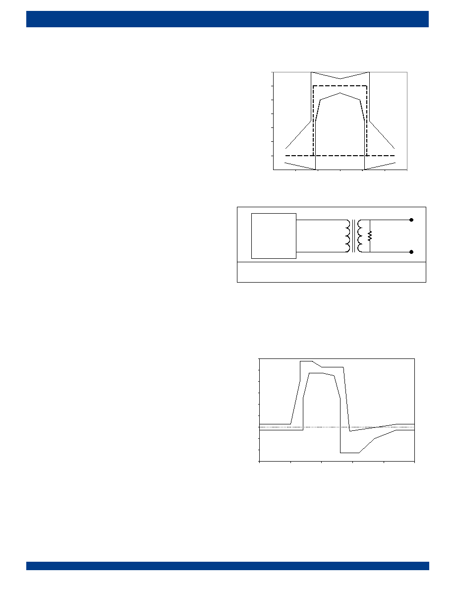
For E1 applications, the pulse shape is shown in
Figure-3
according to
the G.703 and the measuring diagram is shown in
Figure-4
. In internal
impedance matching mode, if the cable impedance is 75
, the PULS[3:0]
bits (TCF1, 03H...) should be set to `0000'; if the cable impedance is 120
, the PULS[3:0] bits (TCF1, 03H...) should be set to `0001'. In external
impedance matching mode, for both E1/75
and E1/120 cable imped-
ance, PULS[3:0] should be set to `0001'.
Figure-3 E1 Waveform Template Diagram
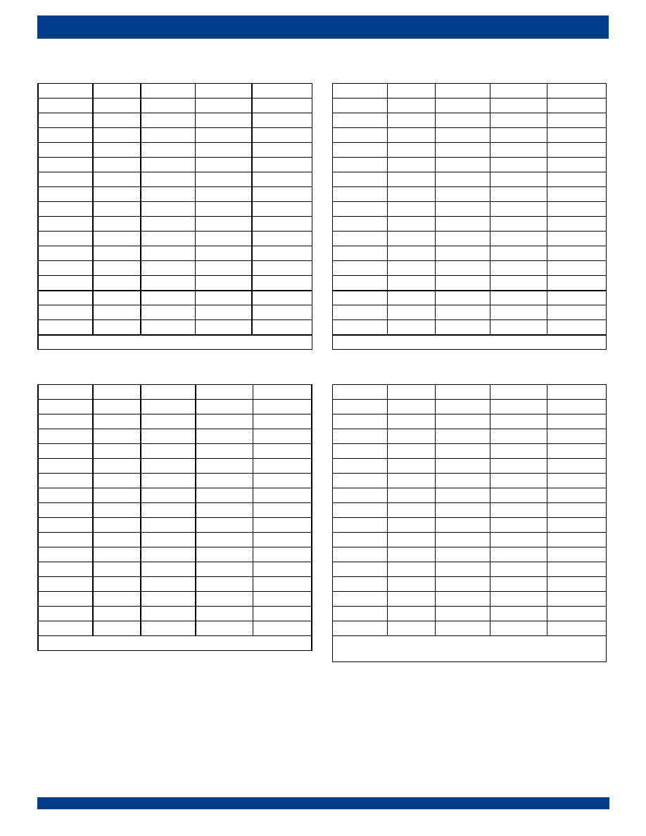
Figure-4 E1 Pulse Template Test Circuit
For T1 applications, the pulse shape is shown in
Figure-5
according to
the T1.102 and the measuring diagram is shown in
Figure-6.
This also
meets the requirement of G.703, 2001. The cable length is divided into five
grades, and there are five pulse templates used for each of the cable length.
The pulse template is selected by PULS[3:0] bits (TCF1, 03H...).
Figure-5 DSX-1 Waveform Template
-0 .6
-0 .4
-0 .2
0
0 .2
0 .4
0 .6
-0 .2 0
0 .0 0
0 .2 0
0 .4 0
0 .6 0
0 .8 0
1 .0 0
1 .2 0
T im e in U n it In te rva ls
N
o
rm
ali
z
ed
Amp
l
i
t
ude
IDT82V2084
V
OUT
R
LOAD
TTIPn
TRINGn
Note: 1. For R
LOAD
= 75
(nom), V
out
(Peak)=2.37V (nom)
2. For R
LOAD
=120
(nom), V
out
(Peak)=3.00V (nom)
-0.6
-0.4
-0.2
0
0.2
0.4
0.6
0.8
1
1.2
0
250
500
750
1000
1250
Time (ns)
Normalized A
m
plitude

15
INDUSTRIAL
TEMPERATURE RANGES
QUAD CHANNEL T1/E1/J1 LONG HAUL/SHORT HAUL LINE INTERFACE UNIT
Figure-6 T1 Pulse Template Test Circuit
For J1 applications, the PULS[3:0] (TCF1, 03H...) should be set to
`0111'.
Table-14
lists these values.
3.2.3.2 LBO (Line Build Out)
To prevent the cross-talk at the far end, the output of TTIP/TRING could
be attenuated before transmission for long haul applications. The FCC Part
68 Regulations specifies four grades of attenuation with a step of 7.5 dB.
Three LBOs are used to implement the pulse attenuation. The PULS[3:0]
bits (TCF1, 03H...) are used to select the attenuation grade. Both
Table-14
and
Table-15
list these values.
3.2.3.3 User-Programmable Arbitrary Waveform
When the PULS[3:0] bits are set to `11xx', user-programmable arbitrary
waveform generator mode can be used in the corresponding channel. This
allows the transmitter performance to be tuned for a wide variety of line con-
dition or special application.
Each pulse shape can extend up to 4 UIs (Unit Interval), addressed by
UI[1:0] bits (TCF3, 05H...) and each UI is divided into 16 sub-phases,
addressed by the SAMP[3:0] bits (TCF3, 05H...). The pulse amplitude of
each phase is represented by a binary byte, within the range from +63 to -
63, stored in WDAT[6:0] bits (TCF4, 06H...) in signed magnitude form. The
most positive number +63 (D) represents the maximum positive amplitude
of the transmit pulse while the most negative number -63 (D) represents the
maximum negative amplitude of the transmit pulse. Therefore, up to 64
bytes are used. For each channel, a 64 bytes RAM is available.
There are twelve standard templates which are stored in a local ROM.
User can select one of them as reference and make some changes to get
the desired waveform.
User can change the wave shape and the amplitude to get the desired
pulse shape. In order to do this, firstly, users can choose a set of waveform
value from the following twelve tables, which is the most similar to the
desired pulse shape.
Table-2
,
Table-3
,
Table-4
,
Table-5
,
Table-6
,
Table-7
,
Table-8
,
Table-9
,
Table-10
,
Table-11
,
Table-12
and
Table-13
list the sample
data and scaling data of each of the twelve templates. Then modify the cor-
responding sample data to get the desired transmit pulse shape.
Secondly, through the value of SCAL[5:0] bits increased or decreased
by 1, the pulse amplitude can be scaled up or down at the percentage ratio
against the standard pulse amplitude if needed. For different pulse shapes,
the value of SCAL[5:0] bits and the scaling percentage ratio are different.
The following twelve tables list these values.
Do the followings step by step, the desired waveform can be pro-
grammed, based on the selected waveform template:
(1).Select the UI by UI[1:0] bits (TCF3, 05H...)
(2).Specify the sample address in the selected UI by SAMP [3:0] bits
(TCF3, 05H...)
(3).Write sample data to WDAT[6:0] bits (TCF4, 06H...). It contains the
data to be stored in the RAM, addressed by the selected UI and the
corresponding sample address.
(4).Set the RW bit (TCF3, 05H...) to `0' to implement writing data to RAM,
or to `1' to implement read data from RAM
(5).Implement the Read from RAM/Write to RAM by setting the DONE
bit (TCF3, 05H...)
Repeat the above steps until all the sample data are written to or read
from the internal RAM.
(6).Write the scaling data to SCAL[5:0] bits (TCF2, 04H...) to scale the
amplitude of the waveform based on the selected standard pulse
amplitude
When more than one UI is used to compose the pulse template, the over-
lap of two consecutive pulses could make the pulse amplitude overflow
(exceed the maximum limitation) if the pulse amplitude is not set properly.
This overflow is captured by DAC_OV_IS bit (INTS1, 17H...), and, if
enabled by the DAC_OV_IM bit (INTM1, 12H...), an interrupt will be gen-
erated.
The following tables give all the sample data based on the preset pulse
templates and LBOs in detail for reference. For preset pulse templates and
LBOs, scaling up/down against the pulse amplitude is not supported.
1.
Table-2
Transmit Waveform Value For E1 75
2.
Table-3
Transmit Waveform Value For E1 120
3.
Table-4
Transmit Waveform Value For T1 0~133 ft
4.
Table-5
Transmit Waveform Value For T1 133~266 ft
5.
Table-6
Transmit Waveform Value For T1 266~399 ft
6.
Table-7
Transmit Waveform Value For T1 399~533 ft
7.
Table-8
Transmit Waveform Value For T1 533~655 ft
8.
Table-9
Transmit Waveform Value For J1 0~655 ft
9.
Table-10
Transmit Waveform Value For DS1 0 dB LBO
10.
Table-11
Transmit Waveform Value For DS1 -7.5 dB LBO
11.
Table-12
Transmit Waveform Value For DS1 -15.0 dB LBO
12.
Table-13
Transmit Waveform Value For DS1 -22.5 dB LBO
IDT82V2084
TTIPn
TRINGn
Cable
R
LOAD
V
OUT
Note: R
LOAD
= 100
± 5%

16
INDUSTRIAL
TEMPERATURE RANGES
QUAD CHANNEL T1/E1/J1 LONG HAUL/SHORT HAUL LINE INTERFACE UNIT
Table-2 Transmit Waveform Value For E1 75
Sample
UI 1
UI 2
UI 3
UI 4
1
0000000
0000000
0000000
0000000
2
0000000
0000000
0000000
0000000
3
0000000
0000000
0000000
0000000
4
0001100
0000000
0000000
0000000
5
0110000
0000000
0000000
0000000
6
0110000
0000000
0000000
0000000
7
0110000
0000000
0000000
0000000
8
0110000
0000000
0000000
0000000
9
0110000
0000000
0000000
0000000
10
0110000
0000000
0000000
0000000
11
0110000
0000000
0000000
0000000
12
0110000
0000000
0000000
0000000
13
0000000
0000000
0000000
0000000
14
0000000
0000000
0000000
0000000
15
0000000
0000000
0000000
0000000
16
0000000
0000000
0000000
0000000
SCAL[5:0] = 100001 (default), One step change of this value of SCAL[5:0]
results in 3% scaling up/down against the pulse amplitude.
Table-3 Transmit Waveform Value For E1 120
Sample
UI 1
UI 2
UI 3
UI 4
1
0000000
0000000
0000000
0000000
2
0000000
0000000
0000000
0000000
3
0000000
0000000
0000000
0000000
4
0001111
0000000
0000000
0000000
5
0111100
0000000
0000000
0000000
6
0111100
0000000
0000000
0000000
7
0111100
0000000
0000000
0000000
8
0111100
0000000
0000000
0000000
9
0111100
0000000
0000000
0000000
10
0111100
0000000
0000000
0000000
11
0111100
0000000
0000000
0000000
12
0111100
0000000
0000000
0000000
13
0000000
0000000
0000000
0000000
14
0000000
0000000
0000000
0000000
15
0000000
0000000
0000000
0000000
16
0000000
0000000
0000000
0000000
SCAL[5:0] = 100001 (default), One step change of this value of SCAL[5:0]
results in 3% scaling up/down against the pulse amplitude.
Table-4 Transmit Waveform Value For T1 0~133 ft
Sample
UI 1
UI 2
UI 3
UI 4
1
0011010
1000010
0000000
0000000
2
0100111
0000000
0000000
0000000
3
0100111
0000000
0000000
0000000
4
0100110
0000000
0000000
0000000
5
0100110
0000000
0000000
0000000
6
0100101
0000000
0000000
0000000
7
0100101
0000000
0000000
0000000
8
0100101
0000000
0000000
0000000
9
0100101
0000000
0000000
0000000
10
1001010
0000000
0000000
0000000
11
1001010
0000000
0000000
0000000
12
1001010
0000000
0000000
0000000
13
1000100
0000000
0000000
0000000
14
1000100
0000000
0000000
0000000
15
1000100
0000000
0000000
0000000
16
1000010
0000000
0000000
0000000
SCAL[5:0] = 110110
1
(default), One step change of this value of SCAL[5:0]
results in 2% scaling up/down against the pulse amplitude.
1. In T1 mode, when arbitrary pulse for short haul application is configured,
users should write `110110' to SCAL[5:0] bits if no scaling is required.
Table-5 Transmit Waveform Value For T1 133~266 ft
Sample
UI 1
UI 2
UI 3
UI 4
1
0011110
1000010
0000000
0000000
2
0101100
0000000
0000000
0000000
3
0101100
0000000
0000000
0000000
4
0101001
0000000
0000000
0000000
5
0101000
0000000
0000000
0000000
6
0101000
0000000
0000000
0000000
7
0100111
0000000
0000000
0000000
8
0100111
0000000
0000000
0000000
9
0100111
0000000
0000000
0000000
10
1001101
0000000
0000000
0000000
11
1001101
0000000
0000000
0000000
12
1001101
0000000
0000000
0000000
13
1000101
0000000
0000000
0000000
14
1000101
0000000
0000000
0000000
15
1000101
0000000
0000000
0000000
16
1000010
0000000
0000000
0000000
See
Table-4
17
INDUSTRIAL
TEMPERATURE RANGES
QUAD CHANNEL T1/E1/J1 LONG HAUL/SHORT HAUL LINE INTERFACE UNIT
Table-6 Transmit Waveform Value For T1 266~399 ft
Sample
UI 1
UI 2
UI 3
UI 4
1
0100100
1000010
0000000
0000000
2
0110001
0000000
0000000
0000000
3
0110001
0000000
0000000
0000000
4
0101110
0000000
0000000
0000000
5
0101011
0000000
0000000
0000000
6
0101010
0000000
0000000
0000000
7
0101010
0000000
0000000
0000000
8
0101001
0000000
0000000
0000000
9
0101001
0000000
0000000
0000000
10
1010010
0000000
0000000
0000000
11
1010010
0000000
0000000
0000000
12
1010010
0000000
0000000
0000000
13
1000111
0000000
0000000
0000000
14
1000111
0000000
0000000
0000000
15
1000111
0000000
0000000
0000000
16
1000010
0000000
0000000
0000000
See
Table-4
Table-7 Transmit Waveform Value For T1 399~533 ft
Sample
UI 1
UI 2
UI 3
UI 4
1
0101010
1000011
0000000
0000000
2
0110100
0000000
0000000
0000000
3
0110100
0000000
0000000
0000000
4
0110100
0000000
0000000
0000000
5
0101110
0000000
0000000
0000000
6
0101101
0000000
0000000
0000000
7
0101100
0000000
0000000
0000000
8
0101011
0000000
0000000
0000000
9
0101011
0000000
0000000
0000000
10
1010110
0000000
0000000
0000000
11
1010110
0000000
0000000
0000000
12
1010110
0000000
0000000
0000000
13
1000111
0000000
0000000
0000000
14
1000111
0000000
0000000
0000000
15
1000111
0000000
0000000
0000000
16
1000011
0000000
0000000
0000000
See
Table-4
Table-8 Transmit Waveform Value For T1 533~655 ft
Sample
UI 1
UI 2
UI 3
UI 4
1
0101101
1000100
0000000
0000000
2
0111000
0000000
0000000
0000000
3
0111000
0000000
0000000
0000000
4
0111000
0000000
0000000
0000000
5
0110001
0000000
0000000
0000000
6
0101110
0000000
0000000
0000000
7
0101101
0000000
0000000
0000000
8
0101100
0000000
0000000
0000000
9
0101100
0000000
0000000
0000000
10
1011010
0000000
0000000
0000000
11
1011010
0000000
0000000
0000000
12
1011010
0000000
0000000
0000000
13
1001010
0000000
0000000
0000000
14
1001000
0000000
0000000
0000000
15
1001000
0000000
0000000
0000000
16
1000100
0000000
0000000
0000000
See
Table-4
Table-9 Transmit Waveform Value For J1 0~655 ft
Sample
UI 1
UI 2
UI 3
UI 4
1
0011010
1000010
0000000
0000000
2
0100111
0000000
0000000
0000000
3
0100111
0000000
0000000
0000000
4
0100110
0000000
0000000
0000000
5
0100110
0000000
0000000
0000000
6
0100101
0000000
0000000
0000000
7
0100101
0000000
0000000
0000000
8
0100101
0000000
0000000
0000000
9
0100101
0000000
0000000
0000000
10
1001010
0000000
0000000
0000000
11
1001010
0000000
0000000
0000000
12
1001010
0000000
0000000
0000000
13
1000100
0000000
0000000
0000000
14
1000100
0000000
0000000
0000000
15
1000100
0000000
0000000
0000000
16
1000010
0000000
0000000
0000000
SCAL[5:0] = 110110 (default), One step change of this value of SCAL[5:0]
results in 2% scaling up/down against the pulse amplitude.
18
INDUSTRIAL
TEMPERATURE RANGES
QUAD CHANNEL T1/E1/J1 LONG HAUL/SHORT HAUL LINE INTERFACE UNIT
Table-10 Transmit Waveform Value For DS1 0 dB LBO
Sample
UI 1
UI 2
UI 3
UI 4
1
0011010
1000010
0000000
0000000
2
0100111
0000000
0000000
0000000
3
0100111
0000000
0000000
0000000
4
0100110
0000000
0000000
0000000
5
0100110
0000000
0000000
0000000
6
0100101
0000000
0000000
0000000
7
0100101
0000000
0000000
0000000
8
0100101
0000000
0000000
0000000
9
0100101
0000000
0000000
0000000
10
1001010
0000000
0000000
0000000
11
1001010
0000000
0000000
0000000
12
1001010
0000000
0000000
0000000
13
1000100
0000000
0000000
0000000
14
1000100
0000000
0000000
0000000
15
1000100
0000000
0000000
0000000
16
1000010
0000000
0000000
0000000
SCAL[5:0] = 110110 (default), One step change of this Value results in 2%
scaling up/down against the pulse amplitude.
Table-11 Transmit Waveform Value For DS1 -7.5 dB LBO
Sample
UI 1
UI 2
UI 3
UI 4
1
0000000
0010100
0000010
0000000
2
0000010
0010010
0000010
0000000
3
0001001
0010000
0000010
0000000
4
0010011
0001110
0000010
0000000
5
0011101
0001100
0000010
0000000
6
0100101
0001011
0000001
0000000
7
0101011
0001010
0000001
0000000
8
0110001
0001001
0000001
0000000
9
0110110
0001000
0000001
0000000
10
0111010
0000111
0000001
0000000
11
0111001
0000110
0000001
0000000
12
0110000
0000101
0000001
0000000
13
0101000
0000100
0000000
0000000
14
0100000
0000100
0000000
0000000
15
0011010
0000011
0000000
0000000
16
0010111
0000011
0000000
0000000
SCAL[5:0] = 010001 (default), One step change of this value of SCAL[5:0]
results in 6.25% scaling up/down against the pulse amplitude.
Table-12 Transmit Waveform Value For DS1 -15.0 dB LBO
Sample
UI 1
UI 2
UI 3
UI 4
1
0000000
0110101
0001111
0000011
2
0000000
0110011
0001101
0000010
3
0000000
0110000
0001100
0000010
4
0000001
0101101
0001011
0000010
5
0000100
0101010
0001010
0000010
6
0001000
0100111
0001001
0000001
7
0001110
0100100
0001000
0000001
8
0010100
0100001
0000111
0000001
9
0011011
0011110
0000110
0000001
10
0100010
0011100
0000110
0000001
11
0101010
0011010
0000101
0000001
12
0110000
0010111
0000101
0000001
13
0110101
0010101
0000100
0000001
14
0110111
0010100
0000100
0000000
15
0111000
0010010
0000011
0000000
16
0110111
0010000
0000011
0000000
SCAL[5:0] = 001000 (default), One step change of the value of SCAL[5:0]
results in 12.5% scaling up/down against the pulse amplitude.
Table-13 Transmit Waveform Value For DS1 -22.5 dB LBO
Sample
UI 1
UI 2
UI 3
UI 4
1
0000001
0110101
0011011
0000111
2
0000011
0110101
0011001
0000110
3
0000101
0110100
0010111
0000110
4
0001000
0110011
0010101
0000101
5
0001100
0110010
0010100
0000101
6
0010001
0110000
0010010
0000101
7
0010110
0101110
0010001
0000100
8
0011011
0101101
0010000
0000100
9
0100001
0101011
0001110
0000100
10
0100110
0101001
0001101
0000100
11
0101010
0100111
0001100
0000011
12
0101110
0100100
0001011
0000011
13
0110001
0100010
0001010
0000011
14
0110011
0100000
0001001
0000011
15
0110100
0011110
0001000
0000011
16
0110100
0011100
0001000
0000010
SCAL[5:0] = 000100 (default), One step change of this value of SCAL[5:0]
results in 25% scaling up/down against the pulse amplitude.
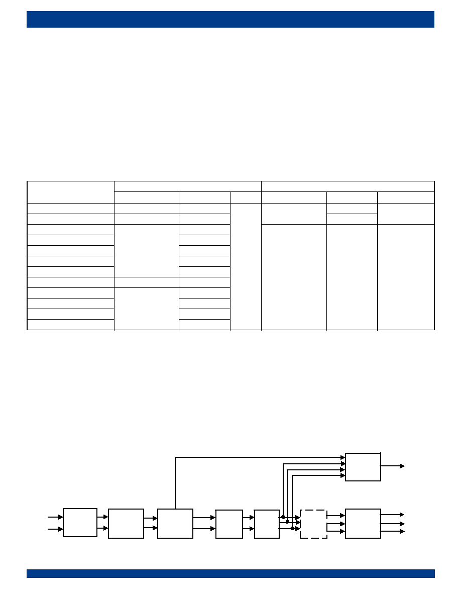
19
INDUSTRIAL
TEMPERATURE RANGES
QUAD CHANNEL T1/E1/J1 LONG HAUL/SHORT HAUL LINE INTERFACE UNIT
3.2.4
TRANSMIT PATH LINE INTERFACE
The transmit line interface consists of TTIPn pin and TRINGn pin. The
impedance matching can be realized by the internal impedance matching
circuit or the external impedance matching circuit. If T_TERM[2] is set to
`0', the internal impedance matching circuit will be selected. In this case,
the T_TERM[1:0] bits (TERM, 1AH...) can be set to choose 75
, 100 ,
110
or 120 internal impedance of TTIPn/TRINGn. If T_TERM[2] is set
to `1', the internal impedance matching circuit will be disabled. In this case,
the external impedance matching circuit will be used to realize the imped-
ance matching. For T1/J1 mode, the external impedance matching circuit
for the transmitter is not supported.
Figure-8
shows the appropriate external
components to connect with the cable for one channel.
Table-14
is the list
of the recommended impedance matching for transmitter.
Note: The precision of the resistors should be better than ± 1%
The TTIPn/TRINGn can be turned into high impedance globally by pull-
ing THZ pin to high or individually by setting the THZ bit (TCF1, 03H...) to
`1'. In this state, the internal transmit circuits are still active.
Besides, in the following cases, TTIPn/TRINGn will also become high
impedance:
∑
Loss of MCLK: all TTIPn/TRINGn pins become high impedance;∑
∑
Loss of TCLKn: corresponding TTIPn/TRINGn become HZ (excep-
tions: Remote Loopback; Transmit internal pattern by MCLK);
∑
Transmit path power down;
∑
After software reset; pin reset and power on.
3.2.5
TRANSMIT PATH POWER DOWN
The transmit path can be powered down individually by setting the
T_OFF bit (TCF0, 02H...) to `1'. In this case, the TTIPn/TRINGn pins are
turned into high impedance.
3.3
RECEIVE PATH
The receive path consists of Receive Internal Termination, Monitor
Gain, Amplitude/Wave Shape Detector, Digital Tuning Controller, Adaptive
Equalizer, Data Slicer, CDR (Clock and Data Recovery), Optional Jitter
Attenuator, Decoder and LOS/AIS Detector. Refer to
Figure-7
.
Figure-7 Receive Path Function Block Diagram
Table-14 Impedance Matching for Transmitter
Cable Configuration
Internal Termination
External Termination
T_TERM[2:0]
PULS[3:0]
R
T
T_TERM[2:0]
PULS[3:0]
R
T
E1/75
000
0000
0
1XX
0001
9.4
E1/120
001
0001
0001
T1/0~133 ft
010
0010
-
-
-
T1/133~266 ft
0011
T1/266~399 ft
0100
T1/399~533 ft
0101
T1/533~655 ft
0110
J1/0~655 ft
011
0111
0 dB LBO
010
1000
-7.5 dB LBO
1001
-15.0 dB LBO
1010
-22.5 dB LBO
1011
Monitor Gain
Adaptive
Equalizer
LOS/AIS
Detector
Data Slicer
Decoder
LOS
RCLK
RDP
RDN
RTIP
Clock
and Data
Recovery
Receive
Internal
termination
RRING
Jitter
Attenuator
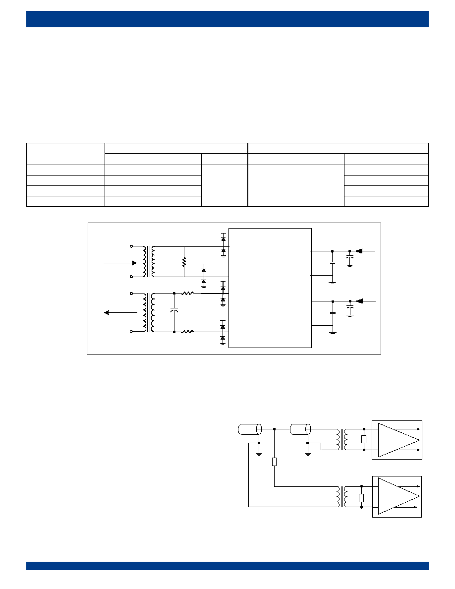
20
INDUSTRIAL
TEMPERATURE RANGES
QUAD CHANNEL T1/E1/J1 LONG HAUL/SHORT HAUL LINE INTERFACE UNIT
3.3.1
RECEIVE INTERNAL TERMINATION
The impedance matching can be realized by the internal impedance
matching circuit or the external impedance matching circuit. If R_TERM[2]
is set to `0', the internal impedance matching circuit will be selected. In this
case, the R_TERM[1:0] bits (TERM, 1AH...) can be set to choose 75
, 100
, 110 or 120 internal impedance of RTIPn/RRINGn. If R_TERM[2]
is set to `1', the internal impedance matching circuit will be disabled. In this
case, the external impedance matching circuit will be used to realize the
impedance matching.
Figure-8
shows the appropriate external components to connect with
the cable for one channel.
Table-15
is the list of the recommended imped-
ance matching for receiver.
Figure-8 Transmit/Receive Line Circuit
3.3.2
LINE MONITOR
In both T1/J1 and E1 short haul applications, the non-intrusive monitor-
ing on channels located in other chips can be performed by tapping the mon-
itored channel through a high impedance bridging circuit. Refer to
Figure-
9
and
Figure-10
.
After a high resistance bridging circuit, the signal arriving at the RTIPn/
RRINGn is dramatically attenuated. To compensate this attenuation, the
Monitor Gain can be used to boost the signal by 22 dB, 26 dB and 32 dB,
selected by MG[1:0] bits (RCF2, 09H...). For normal operation, the Monitor
Gain should be set to 0 dB.
Figure-9 Monitoring Receive Line in Another Chip
Table-15 Impedance Matching for Receiver
Cable Configuration
Internal Termination
External Termination
R_TERM[2:0]
R
R
R_TERM[2:0]
R
R
E1/75
000
120
1XX
75
E1/120
001
120
T1
010
100
J1
011
110
∑
∑
∑ ∑
R
X
Line
R
R
∑
∑
T
X
Line
R
T
R
T
RTIPn
RRINGn
TRINGn
TTIPn
ID
T
8
2V
208
4
One of the Four Identical Channels
VDDTn
VDDTn
D4
D3
D2
D1
1:1
2:1
A
B
∑
∑
D6
D5
∑
D8
D7
∑
Cp
VDDRn
VDDRn
2
3
∑
0.1
µF
GNDTn
VDDTn
68
µF
1
3.3 V
∑
0.1
µF
GNDRn
VDDRn
68
µF
3.3 V
1
Note: 1. Common decoupling capacitor
2. Cp 0-560 (pF)
3. D1 - D8, Motorola - MBR0540T1; International Rectifier - 11DQ04 or 10BQ060
∑
∑
∑
∑
RTIP
RRING
RTIP
RRING
normal receive mode
monitor mode
DSX cross connect
point
R
monitor gain
=22/26/32dB
monitor
gain=0dB

21
INDUSTRIAL
TEMPERATURE RANGES
QUAD CHANNEL T1/E1/J1 LONG HAUL/SHORT HAUL LINE INTERFACE UNIT
Figure-10 Monitor Transmit Line in Another Chip
3.3.3
ADAPTIVE EQUALIZER
The adaptive equalizer can remove most of the signal distortion due to
intersymbol interference caused by cable attenuation. It can be enabled or
disabled by setting EQ_ON bit to `1' or `0' (RCF1, 08H...).
When the adaptive equalizer is out of range, EQ_S bit (STAT0, 14H...)
will be set to `1' to indicate the status of equalizer. If EQ_IES bit (INTES,
13H...) is set to `1', any changes of EQ_S bit will generate an interrupt and
EQ_IS bit (INTS0, 16H...) will be set to `1' if it is not masked. If EQ_IES bit
is set to `0', only the `0' to `1' transition of the EQ_S bit will generate an inter-
rupt and EQ_IS bit will be set to `1' if it is not masked. The EQ_IS bit will be
reset after being read.
The Amplitude/wave shape detector keeps on measuring the ampli-
tude/wave shape of the incoming signals during an observation period. This
observation period can be 32, 64, 128 or 256 symbol periods, as selected
by UPDW[1:0] bits (RCF2, 09H...). A shorter observation period allows
quicker response to pulse amplitude variation while a longer observation
period can minimize the possible overshoots. The default observation
period is 128 symbol periods.
Based on the observed peak value for a period, the equalizer will be
adjusted to achieve a normalized signal. LATT[4:0] bits (STAT1, 15H...)
indicate the signal attenuation introduced by the cable in approximately 2
dB per step.
3.3.4
RECEIVE SENSITIVITY
For short haul application, the Receive Sensitivity for both E1 and T1/
J1 is -10 dB. For long haul application, the receive sensitivity is -43 dB for
E1 and -36 dB for T1/J1.
3.3.5
DATA SLICER
The Data Slicer is used to generate a standard amplitude mark or a
space according to the amplitude of the input signals. The threshold can
be 40%, 50%, 60% or 70%, as selected by the SLICE[1:0] bits (RCF2,
09H...). The output of the Data Slicer is forwarded to the CDR (Clock & Data
Recovery) unit or to the RDPn/RDNn pins directly if the CDR is disabled.
3.3.6
CDR (Clock & Data Recovery)
The CDR is used to recover the clock from the received signals. The
recovered clock tracks the jitter in the data output from the Data Slicer and
keeps the phase relationship between data and clock during the absence
of the incoming pulse. The CDR can also be by-passed in the Dual Rail
mode. When CDR is by-passed, the data from the Data Slicer is output to
the RDPn/RDNn pins directly.
3.3.7
DECODER
In T1/J1 applications, the R_MD[1:0] bits (RCF0, 07H...) is used to
select the AMI decoder or B8ZS decoder. In E1 applications, the R_MD[1:0]
bits (RCF0, 07H...) are used to select the AMI decoder or HDB3 decoder.
3.3.8
RECEIVE PATH SYSTEM INTERFACE
The receive path system interface consists of RCLKn pin, RDn/RDPn
pin and RDNn pin. In E1 mode, the RCLKn outputs a recovered 2.048 MHz
clock. In T1/J1 mode, the RCLKn outputs a recovered 1.544 MHz clock. The
received data is updated on the RDn/RDPn and RDNn pins on the active
edge of RCLKn. The active edge of RCLKn can be selected by the
RCLK_SEL bit (RCF0, 07H...). And the active level of the data on RDn/
RDPn and RDNn can also be selected by the RD_INV bit (RCF0, 07H...).
The received data can be output to the system side in two different ways:
Single Rail or Dual Rail, as selected by R_MD bit [1] (RCF0, 07H...). In Sin-
gle Rail mode, only RDn pin is used to output data and the RDNn/CVn pin
is used to report the received errors. In Dual Rail Mode, both RDPn pin and
RDNn pin are used for outputting data.
In the receive Dual Rail mode, the CDR unit can be by-passed by setting
R_MD[1:0] to `11' (binary). In this situation, the output data from the Data
Slicer will be output to the RDPn/RDNn pins directly, and the RCLKn out-
puts the exclusive OR (XOR) of the RDPn and RDNn.
3.3.9
RECEIVE PATH POWER DOWN
The receive path can be powered down individually by setting R_OFF
bit (RCF0, 07H...) to `1'. In this case, the RCLKn, RDn/RDPn, RDPn and
LOSn will be logic low.
3.3.10 G.772 NON-INTRUSIVE MONITORING
In applications using only three channels, channel 1 can be configured
to monitor the data received or transmitted in any one of the remaining chan-
nels. The MON[3:0] bits (GCF1, 60H) determine which channel and which
direction (transmit/receive) will be monitored. The monitoring is non-intru-
sive per ITU-T G.772.
Figure-11
illustrates the concept.
The monitored line signal (transmit or receive) goes through Channel
1's Clock and Data Recovery. The signal can be observed digitally at the
RCLK1, RD1/RDP1 and RDN1. If Channel 1 is configured to Remote Loop-
back while in the Monitoring mode, the monitored data will be output on
TTIP1/TRING1.
TTIP
TRING
RTIP
RRING
normal transmit mode
monitor mode
DSX cross connect
point
R
monitor gain
monitor gain
=22/26/32dB
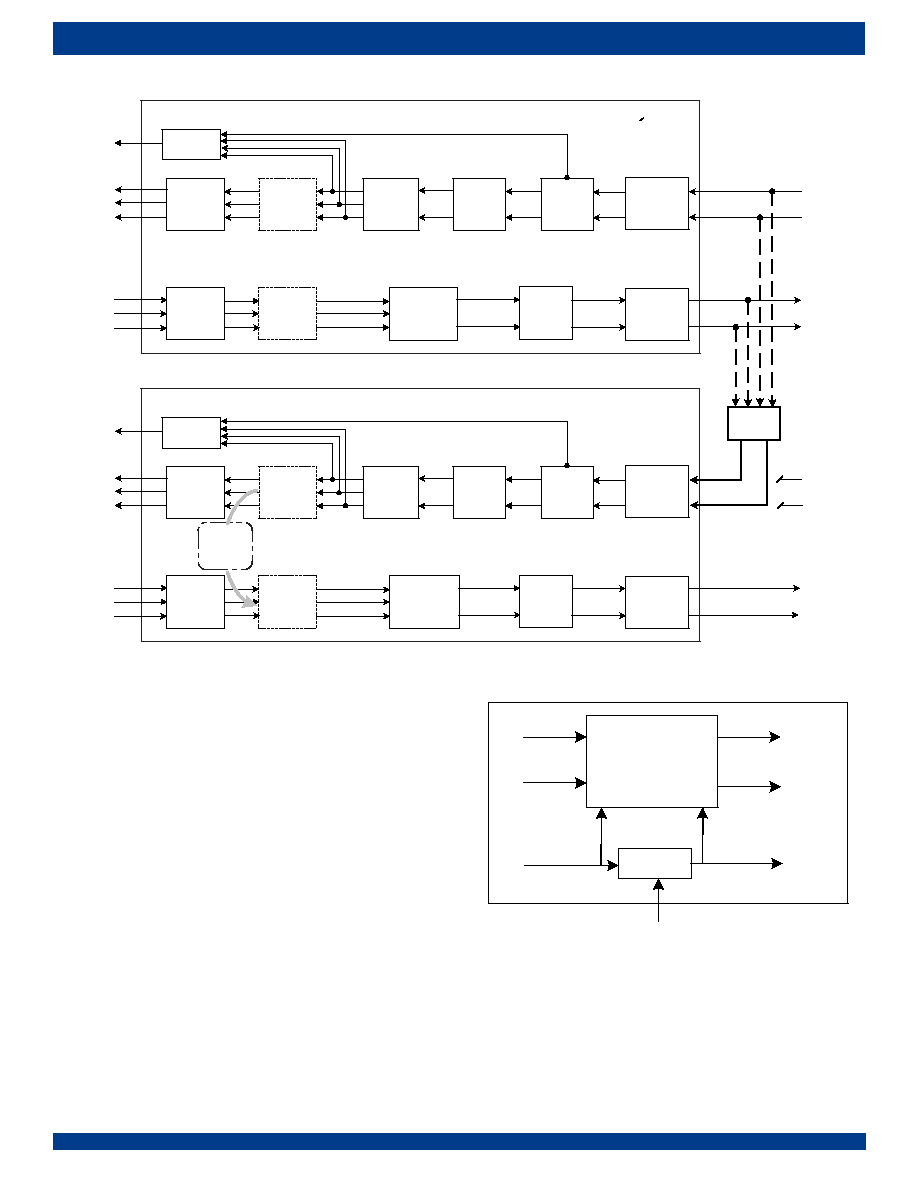
22
INDUSTRIAL
TEMPERATURE RANGES
QUAD CHANNEL T1/E1/J1 LONG HAUL/SHORT HAUL LINE INTERFACE UNIT
Figure-11 G.772 Monitoring Diagram
3.4
JITTER ATTENUATOR
There is one Jitter Attenuator in each channel of the LIU. The Jitter Atten-
uator can be deployed in the transmit path or the receive path, and can also
be disabled. This is selected by the JACF[1:0] bits (JACF, 01H...).
3.4.1
JITTER ATTENUATION FUNCTION DESCRIPTION
The Jitter Attenuator is composed of a FIFO and a DPLL, as shown in
Figure-12
. The FIFO is used as a pool to buffer the jittered input data, then
the data is clocked out of the FIFO by a de-jittered clock. The depth of the
FIFO can be 32 bits, 64 bits or 128 bits, as selected by the JADP[1:0] bits
(JACF, 01H...). Consequently, the constant delay of the Jitter Attenuator
will be 16 bits, 32 bits or 64 bits. Deeper FIFO can tolerate larger jitter, but
at the expense of increasing data latency time.
Figure-12 Jitter Attenuator
In E1 applications, the Corner Frequency of the DPLL can be 0.9 Hz or
6.8 Hz, as selected by the JABW bit (JACF, 01H...). In T1/J1 applications,
the Corner Frequency of the DPLL can be 1.25 Hz or 5.00 Hz, as selected
by the JABW bit (JACF, 01H...). The lower the Corner Frequency is, the
longer time is needed to achieve synchronization.
When the incoming data moves faster than the outgoing data, the FIFO
will overflow. This overflow is captured by the JAOV_IS bit (INTS1, 17H...).
Channel N (N > 2)
B8ZS/
HDB3/AMI
Encoder
Jitter
Attenuator
Line
Driver
Waveform
Shaper/LBO
B8ZS/
HDB3/AMI
Decoder
Jitter
Attenuator
Data
Slicer
Adaptive
Equalizer
LOS/AIS
Detector
Clock and
Data
Recovery
Transmitter
Internal
Termination
Receiver
Internal
Termination
TCLKn
TDNn
TDn/TDPn
RCLKn
CVn/RDNn
LOSn
RDn/RDPn
RRINGn
TTIPn
TRINGn
RTIPn
Channel 1
B8ZS/
HDB3/AMI
Encoder
Jitter
Attenuator
Line
Driver
Waveform
Shaper/LBO
B8ZS/
HDB3/AMI
Decoder
Jitter
Attenuator
Data
Slicer
Adaptive
Equalizer
LOS/AIS
Detector
Clock and
Data
Recovery
Transmitter
Internal
Termination
Receiver
Internal
Termination
TCLK1
TDN1
TDn/TDP1
RCLK1
CVn/RDN1
LOS1
RDn/RDP1
RRING1
TTIP1
TRING1
RTIP1
Remote
Loopback
G.772
Monitor
FIFO
32/64/128
DPLL
Jittered Data
De-jittered Data
Jittered Clock
De-jittered Clock
MCLK
W
R
RCLKn
RDn/RDPn
RDNn
23
INDUSTRIAL
TEMPERATURE RANGES
QUAD CHANNEL T1/E1/J1 LONG HAUL/SHORT HAUL LINE INTERFACE UNIT
If the incoming data moves slower than the outgoing data, the FIFO will
underflow. This underflow is captured by the
JAUD_IS
bit (INTS1, 17H...).
For some applications that are sensitive to data corruption, the JA limit
mode can be enabled by setting JA_LIMIT bit (JACF, 01H...) to `1'. In the
JA limit mode, the speed of the outgoing data will be adjusted automatically
when the FIFO is close to its full or emptiness. The criteria of starting speed
adjustment are shown in
Table-16
. The JA limit mode can reduce the pos-
sibility of FIFO overflow and underflow, but the quality of jitter attenuation
is deteriorated.
3.4.2
JITTER ATTENUATOR PERFORMANCE
The performance of the Jitter Attenuator in the IDT82V2084 meets the
ITU-T I.431, G.703, G.736-739, G.823, G.824, ETSI 300011, ETSI TBR12/
13, AT&T TR62411 specifications. Details of the Jitter Attenuator perfor-
mance is shown in
Table-68 Jitter Tolerance
and
Table-69 Jitter Attenuator
Characteristics
.
3.5
LOS AND AIS DETECTION
3.5.1
LOS DETECTION
The Loss of Signal Detector monitors the amplitude of the incoming sig-
nal level and pulse density of the received signal on RTIPn and RRINGn.
∑ LOS declare (LOS=1)
A LOS is detected when the incoming signal has "no transitions", i.e.,
when the signal level is less than Q dB below nominal for N consecutive
pulse intervals. Here N is defined by LAC bit (MAINT0, 0AH...). LOS will be
declared by pulling LOSn pin to high (LOS=1) and LOS interrupt will be gen-
erated if it is not masked.
∑ LOS clear (LOS=0)
The LOS is cleared when the incoming signal has "transitions", i.e.,
when the signal level is greater than P dB below nominal and has an aver-
age pulse density of at least 12.5% for M consecutive pulse intervals, start-
ing with the receipt of a pulse. Here M is defined by LAC bit (MAINT0,
0AH...). LOS status is cleared by pulling LOSn pin to low.
Figure-13 LOS Declare and Clear
∑ LOS detect level threshold
In short haul mode, the amplitude threshold Q is fixed on 800 mVpp,
while P=Q+200 mVpp (200 mVpp is the LOS level detect hysteresis).
In long haul mode, the value of Q can be selected by LOS[4:0] bit
(RCF1, 08H...), while P=Q+4 dB (4 dB is the LOS level detect hysteresis).
The LOS[4:0] default value is 10101 (-46 dB).
∑ Criteria for declare and clear of a LOS detect
The detection supports the ANSI T1.231 and I.431 for T1/J1 mode and
G.775 and ETSI 300233/I.431 for E1 mode. The criteria can be selected
by LAC bit (MAINT0, 0AH...) and T1E1 bit (GCF0, 40H).
Table-17
and
Table-18
summarize LOS declare and clear criteria for
both short haul and long haul application.
∑ All Ones output during LOS
On the system side, the RDPn/RDNn will reflect the input pulse "transi-
tion" at the RTIPn/RRINGn side and output recovery clock (but the quality
of the output clock can not be guaranteed when the input level is lower than
the maximum receive sensitivity) when AISE bit (MAINT0, 0AH...) is 0; or
output All Ones as AIS when AISE bit (MAINT0, 0AH...) is 1. In this case
RCLKn output is replaced by MCLK.
On the line side, the TTIPn/TRINGn will output All Ones as AIS when
ATAO bit (MAINT0, 0AH...) is 1. The All Ones pattern uses MCLK as the
reference clock.
LOS indicator is always active for all kinds of loopback modes.
Table-16 Criteria of Starting Speed Adjustment
FIFO Depth
Criteria for Adjusting Data Outgoing Speed
32 Bits
2 bits close to its full or emptiness
64 Bits
3 bits close to its full or emptiness
128 Bits
4 bits close to its full or emptiness
signal level<Q
(observing windows= N)
(observing windows= M)
signal level>P
density=OK
LOS=1
LOS=0

24
INDUSTRIAL
TEMPERATURE RANGES
QUAD CHANNEL T1/E1/J1 LONG HAUL/SHORT HAUL LINE INTERFACE UNIT
Table-17 LOS Declare and Clear Criteria for Short Haul Mode
Control bit
LOS declare threshold
LOS clear threshold
T1E1
LAC
1=T1/J1
0=T1.231
Level < 800 mVpp
N=175 bits
Level > 1 Vpp
M=128 bits
12.5% mark density
<100 consecutive zeroes
1=I.431
Level < 800 mVpp
N=1544 bits
Level > 1 Vpp
M=128 bits
12.5% mark density
<100 consecutive zeroes
0=E1
0=G.775
Level < 800 mVpp
N=32 bits
Level > 1 Vpp
M=32 bits
12.5% mark density
<16 consecutive zeroes
1=I.431/ETSI
Level < 800 mVpp
N=2048 bits
Level > 1 Vpp
M=32 bits
12.5% mark density
<16 consecutive zeroes

25
INDUSTRIAL
TEMPERATURE RANGES
QUAD CHANNEL T1/E1/J1 LONG HAUL/SHORT HAUL LINE INTERFACE UNIT
3.5.2
AIS DETECTION
The Alarm Indication Signal can be detected by the IDT82V2084 when
the Clock&Data Recovery unit is enabled. The status of AIS detection is
reflected in the AIS_S bit (STAT0, 14H...). In T1/J1 applications, the criteria
for declaring/clearing AIS detection are in compliance with the ANSI
T1.231. In E1 applications, the criteria for declaring/clearing AIS detection
comply with the ITU G.775 or the ETSI 300233, as selected by the LAC bit
(MAINT0, 0AH...).
Table-19
summarizes different criteria for AIS detection
Declaring/Clearing.
Table-18 LOS Declare and Clear Criteria for Long Haul Mode
Control bit
LOS declare threshold
LOS clear threshold
Note
T1E1
LAC
LOS[4:0]
Q (dB)
1=T1/J1
0
T1.231
00000
00001
...
10001
...
10101
10110-11111
-4
-6
...
-38
...
-46
-48
Level < Q
N=175 bits
Level > Q+ 4dB
M=128 bits
12.5% mark density
<100 consecutive zeroes
1
-
00000
...
00110
-4
-16
Level < Q
N=1544 bits
Level > Q+ 4dB
M=128 bits
12.5% mark density
<100 consecutive zeroes
I.431 Level detect range is -18 to -30 dB.
I.431 00111
...
01101
-18
...
-30
-
01110
...
10001
...
10101
10110-11111
-32
...
-38
...
-46
-48
0=E1
0
-
00000
...
00010
-4
...
-8
Level < Q
N=32 bits
Level > Q+ 4dB
M=32 bits
12.5% mark density
<16 consecutive zeroes
G.775 Level detect range is -9 to -35 dB.
G.775
00011
...
10000
-10
...
-36
-
10001
...
10101(default)
10110-11111
-38
...
-46
-48
1
-
00000
-4
Level < Q
N=2048 bits
Level > Q+ 4dB
M=32 bits
12.5% mark density
<16 consecutive zeroes
I.431 Level detect range is -6 to -20 dB.
I.431/
ETSI
00001
...
01000
-6
...
-20
-
01001
...
10101(default)
10110-11111
-22
...
-46
-48
Table-19 AIS Condition
ITU G.775 for E1
(LAC bit is set to `0' by default)
ETSI 300233 for E1
(LAC bit is set to `1')
ANSI T1.231 for T1/J1
AIS
detected
Less than 3 zeros contained in each of two consecutive
512-bit streams are received
Less than 3 zeros contained in a 512-bit
stream are received
Less than 9 zeros contained in an 8192-bit stream
(a ones density of 99.9% over a period of 5.3ms)
AIS
cleared
3 or more zeros contained in each of two consecutive
512-bit streams are received
3 or more zeros contained in a 512-bit
stream are received
9 or more zeros contained in an 8192-bit stream
are received

26
INDUSTRIAL
TEMPERATURE RANGES
QUAD CHANNEL T1/E1/J1 LONG HAUL/SHORT HAUL LINE INTERFACE UNIT
3.6
TRANSMIT AND DETECT INTERNAL PATTERNS
The internal patterns (All Ones, All Zeros, PRBS/QRSS pattern and
Activate/Deactivate Loopback Code) will be generated and detected by the
IDT82V2084. TCLKn is used as the reference clock by default. MCLK can
also be used as the reference clock by setting the PATT_CLK bit (MAINT0,
0AH...) to `1'.
If the PATT_CLK bit (MAINT0, 0AH...) is set to `0' and the PATT[1:0] bits
(MAINT0, 0AH...) are set to `00', the transmit path will operate in normal
mode.
3.6.1
TRANSMIT ALL ONES
In transmit direction, the All Ones data can be inserted into the data
stream when the PATT[1:0] bits (MAINT0, 0AH...) are set to `01'. The trans-
mit data stream is output from TTIPn/TRINGn. In this case, either TCLKn
or MCLK can be used as the transmit clock, as selected by the PATT_CLK
bit (MAINT0, 0AH...).
3.6.2
TRANSMIT ALL ZEROS
If the PATT_CLK bit (MAINT0, 0AH...) is set to `1', the All Zeros will be
inserted into the transmit data stream when the PATT[1:0] bits (MAINT0,
0AH...) are set to `00'.
3.6.3
PRBS/QRSS GENERATION AND DETECTION
A PRBS/QRSS will be generated in the transmit direction and detected
in the receive direction by IDT82V2084. The QRSS is 2
20
-1 for T1/J1 appli-
cations and the PRBS is 2
15
-1 for E1 applications, with maximum zero
restrictions according to the AT&T TR62411 and ITU-T O.151.
When the PATT[1:0] bits (MAINT0, 0AH...) are set to `10', the PRBS/
QRSS pattern will be inserted into the transmit data stream with the MSB
first. The PRBS/QRSS pattern will be transmitted directly or invertedly.
The PRBS/QRSS in the received data stream will be monitored. If the
PRBS/QRSS has reached synchronization status, the PRBS_S bit
(STAT0, 14H...) will be set to `1', even in the presence of a logic error rate
less than or equal to 10
-1
. The criteria for setting/clearing the PRBS_S bit
are shown in
Table-20
.
PRBS data can be inverted through setting the PRBS_INV bit (MAINT0,
0AH...).
Any change of PRBS_S bit will be captured by PRBS_IS bit (INTS0,
16H...). The PRBS_IES bit (INTES, 13H...) can be used to determine
whether the `0' to `1' change of PRBS_S bit will be captured by the PRBS_IS
bit or any changes of PRBS_S bit will be captured by the PRBS_IS bit. When
the PRBS_IS bit is `1', an interrupt will be generated if the PRBS_IM bit
(INTM0, 11H...) is set to `1'.
The received PRBS/QRSS logic errors can be counted in a 16-bit
counter if the ERR_SEL [1:0] bits (MAINT6, 10H...) are set to `00'. Refer to
Refer to
3.8 ERROR DETECTION/COUNTING AND INSERTION
for the
operation of the error counter.
3.7
LOOPBACK
To facilitate testing and diagnosis, the IDT82V2084 provides four dif-
ferent loopback configurations: Analog Loopback, Digital Loopback,
Remote Loopback and Inband Loopback.
3.7.1
ANALOG LOOPBACK
When the ALP bit (MAINT1, 0BH...) is set to `1', the corresponding chan-
nel is configured in Analog Loopback mode. In this mode, the transmit sig-
nals are looped back to the Receiver Internal Termination in the receive
path then output from RCLKn, RDn, RDPn/RDNn. At the same time, the
transmit signals are still output to TTIPn/TRINGn in transmit direction.
Fig-
ure-14
shows the process.
Figure-14 Analog Loopback
3.7.2
DIGITAL LOOPBACK
When the DLP bit (MAINT1, 0BH...) is set to `1', the corresponding chan-
nel is configured in Digital Loopback mode. In this mode, the transmit sig-
nals are looped back to the jitter attenuator (if enabled) and decoder in
receive path, then output from RCLKn, RDn, RDPn/RDNn. At the same
time, the transmit signals are still output to TTIPn/TRINGn in transmit direc-
tion.
Figure-15
shows the process.
Table-20 Criteria for Setting/Clearing the PRBS_S Bit
PRBS/QRSS
Detection
6 or less than 6 bit errors detected in a 64 bits hopping window.
PRBS/QRSS
Missing
More than 6 bit errors detected in a 64 bits hopping window.
One of the Four Identical Channels
B8ZS/
HDB3/AMI
Encoder
Jitter
Attenuator
Line
Driver
Waveform
Shaper/LBO
B8ZS/
HDB3/AMI
Decoder
Jitter
Attenuator
Data
Slicer
Adaptive
Equalizer
LOS/AIS
Detector
Clock and
Data
Recovery
Transmitter
Internal
Termination
Receiver
Internal
Termination
TCLKn
TDNn
TDn/TDPn
RCLKn
CVn/RDNn
LOSn
RDn/RDPn
RRINGn
TTIPn
TRINGn
RTIPn
Analog
Loopback
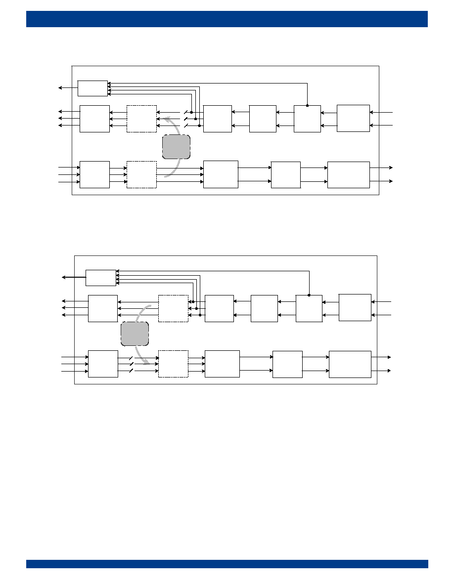
27
INDUSTRIAL
TEMPERATURE RANGES
QUAD CHANNEL T1/E1/J1 LONG HAUL/SHORT HAUL LINE INTERFACE UNIT
Both Analog Loopback mode and Digital Loopback mode allow the
sending of the internal patterns (All Ones, All Zeros, PRBS, etc.) which will
overwrite the transmit signals. In this case, either TCLKn or MCLK can be
used as the reference clock for internal patterns transmission.
Figure-15 Digital Loopback
3.7.3
REMOTE LOOPBACK
When the RLP bit (MAINT1, 0BH...) is set to `1', the corresponding chan-
nel is configured in Remote Loopback mode. In this mode, the recovered
clock and data output from Clock and Data Recovery on the receive path
is looped back to the jitter attenuator (if enabled) and Waveform Shaper in
transmit path.
Figure-16
shows the process.
Figure-16 Remote Loopback
3.7.4
INBAND LOOPBACK
When PATT[1:0] bits
(MAINT0, 0AH...) are set to `11', the correspond-
ing channel is configured in Inband Loopback mode. In this mode, an
unframed activate/Deactivate Loopback Code is generated repeatedly in
transmit direction per ANSI T1. 403 which overwrite the transmit signals.
In receive direction, the framed or unframed code is detected per ANSI T1.
403, even in the presence of 10
-2
bit error rate.
If the Automatic Remote Loopback is enabled by setting ARLP bit
(MAINT1, 0BH...) to `1', the chip will establish/demolish the Remote Loop-
back based on the reception of the Activate Loopback Code/Deactivate
Loopback Code for 5.1 s. If the ARLP bit (MAINT1, 0BH...) is set to `0', the
Remote Loopback can also be demolished forcedly.
3.7.4.1 Transmit Activate/Deactivate Loopback Code
The pattern of the transmit Activate/Deactivate Loopback Code is
defined by the TIBLB[7:0] bits (MAINT3, 0DH...). Whether the code repre-
sents an Activate Loopback Code or a Deactivate Loopback Code is judged
by the far end receiver. The length of the pattern ranges from 5 bits to 8 bits,
as selected by the TIBLB_L[1:0] bits (MAINT2, 0CH...). The pattern can be
programmed to 6-bit-long or 8-bit-long respectively by repeating itself if it
is 3-bit-long or 4-bit-long. When the PATT[1:0] bits (MAINT0, 0AH...) are
set to `11', the transmission of the Activate/Deactivate Loopback Code is
initiated. If the PATT_CLK bit (MAINT0, 0AH...) is set to `0' and the
PATT[1:0] bits (MAINT0, 0AH...) are set to `00', the transmission of the Acti-
vate/Deactivate Loopback Code will stop.
The local transmit activate/deactivate code setting should be the same
as the receive code setting in the remote end. It is the same thing for the
other way round.
One of the Four Identical Channels
B8ZS/
HDB3/AMI
Encoder
Jitter
Attenuator
B8ZS/
HDB3/AMI
Decoder
Jitter
Attenuator
Data
Slicer
Adaptive
Equalizer
LOS/AIS
Detector
Clock and
Data
Recovery
Digital
Loopback
Receiver
Internal
Termination
TCLKn
TDNn
TDn/TDPn
RCLKn
CVn/RDNn
LOSn
RDn/RDPn
RRINGn
TTIPn
TRINGn
RTIPn
Line
Driver
Waveform
Shaper/LBO
Transmitter
Internal
Termination
One of the Four Identical Channels
B8ZS/
HDB3/AMI
Encoder
Jitter
Attenuator
B8ZS/
HDB3/AMI
Decoder
Jitter
Attenuator
Data
Slicer
Adaptive
Equalizer
LOS/AIS
Detector
Clock and
Data
Recovery
Receiver
Internal
Termination
TCLKn
TDNn
TDn/TDPn
RCLKn
CVn/RDNn
LOSn
RDn/RDPn
RRINGn
TTIPn
TRINGn
RTIPn
Remote
Loopback
Line
Driver
Waveform
Shaper/LBO
Transmitter
Internal
Termination

28
INDUSTRIAL
TEMPERATURE RANGES
QUAD CHANNEL T1/E1/J1 LONG HAUL/SHORT HAUL LINE INTERFACE UNIT
3.7.4.2 Receive Activate/Deactivate Loopback Code
The pattern of the receive Activate Loopback Code is defined by the
RIBLBA[7:0] bits (MAINT4, 0EH...). The length of this pattern ranges from
5 bits to 8 bits, as selected by the RIBLBA_L [1:0] bits (MAINT2, 0CH...).
The pattern can be programmed to 6-bit-long or 8-bit-long respectively by
repeating itself if it is 3-bit-long or 4-bit-long.
The pattern of the receive Deactivate Loopback Code is defined by the
RIBLBD[7:0] bits (MAINT5, 0FH...). The length of the receive Deactivate
Loopback Code ranges from 5 bits to 8 bits, as selected by the
RIBLBD_L[1:0] bits (MAINT2, 0CH...). The pattern can be programmed to
6-bit-long or 8-bit-long respectively by repeating itself if it is 3-bit-long or 4-
bit-long.
After the Activate Loopback Code has been detected in the receive data
for more than 30 ms (in E1 mode) / 40 ms (in T1/J1 mode), the IBLBA_S
bit (STAT0, 14H...) will be set to `1' to declare the reception of the Activate
Loopback Code.
After the Deactivate Loopback Code has been detected in the receive
data for more than 30 ms (In E1 mode) / 40 ms (In T1/J1 mode), the IBLBD_S
bit (STAT0, 14H...) will be set to `1' to declare the reception of the Deactivate
Loopback Code.
When the IBLBA_IES bit (INTES, 13H...) is set to `0', only the `0' to `1'
transition of the IBLBA_S bit will generate an interrupt and set the IBLBA_IS
bit (INTS0, 16H...) to `1'. When the IBLBA_IES bit is set to `1', any changes
of the IBLBA_S bit will generate an interrupt and set the IBLBA_IS bit
(INTS0, 16H...) to `1'. The IBLBA_IS bit will be reset to `0' after being read.
When the IBLBD_IES bit (INTES, 13H...) is set to `0', only the `0' to `1'
transition of the IBLBD_S bit will generate an interrupt and set the IBLBD_IS
bit (INTS0, 16H...) to `1'. When the IBLBD_IES bit is set to `1', any changes
of the IBLBD_S bit will generate an interrupt and set the IBLBD_IS bit
(INTS0, 16H...) to `1'. The IBLBD_IS bit will be reset to `0' after being read.
3.7.4.3 Automatic Remote Loopback
When ARLP bit (MAINT1, 0BH...) is set to `1', the corresponding chan-
nel is configured into the Automatic Remote Loopback mode. In this mode,
if the Activate Loopback Code has been detected in the receive data for
more than 5.1 s, the Remote Loopback (shown as
Figure-16
) will be estab-
lished automatically, and the RLP_S bit (STAT1, 15H...) will be set to `1' to
indicate the establishment of the Remote Loopback. The IBLBA_S bit
(STAT0, 14H...) is set to `1' to generate an interrupt. In this case, the Remote
Loopback mode will still be kept even if the receiver stop receiving the Acti-
vate Loopback Code.
If the Deactivate Loopback Code has been detected in the receive data
for more than 5.1 s, the Remote Loopback will be demolished automatically,
and the RLP_S bit (STAT1, 15H...) will set to `0' to indicate the demolish-
ment of the Remote Loopback. The IBLBD_S bit (STAT0, 14H...) is set to
`1' to generate an interrupt.
The Remote Loopback can also be demolished forcedly by setting
ARLP bit (MAINT1, 0BH...) to `0'.
3.8
ERROR DETECTION/COUNTING AND INSERTION
3.8.1
DEFINITION OF LINE CODING ERROR
The following line encoding errors can be detected and counted by the
IDT82V2084:
∑
Received Bipolar Violation (BPV) Error: In AMI coding, when two
consecutive pulses of the same polarity are received, a BPV error
is declared.
∑
HDB3/B8ZS Code Violation (CV) Error: In HDB3/B8ZS coding, a
CV error is declared when two consecutive BPV errors are
detected, and the pulses that have the same polarity as the previ-
ous pulse are not the HDB3/B8ZS zero substitution pulses.
∑
Excess Zero (EXZ) Error: there are two standards defining the EXZ
errors: ANSI and FCC. The EXZ_DEF bit (MAINT6, 10H...)
chooses which standard will be adopted by the corresponding
channel to judge the EXZ error.
Table-21
shows definition of EXZ.
3.8.2
ERROR DETECTION AND COUNTING
Which type of the receiving errors (Received CV/BPV errors, excess
zero errors and PRBS logic errors) will be counted is determined by
ERR_SEL[1:0] bits (MAINT6, 10H...). Only one type of receiving errors can
be counted at a time. When the ERR_SEL[1:0] bits are set to `11', no receiv-
ing errors will be detected and counted.
The selected type of receiving errors is counted in an internal 16-bit Error
Counter. Once an error is detected, an error interrupt which is indicated by
corresponding bit in (INTS1, 17H...) will be generated if it is not masked.
This Error Counter can be operated in two modes: Auto Report Mode and
Manual Report Mode, as selected by the CNT_MD bit (MAINT6, 10H...).
In Single Rail mode, once BPV or CV errors are detected, the CVn pin will
be driven to high for one RCLK period.
∑ Auto Report Mode
In Auto Report Mode, the internal counter starts to count the received
errors when the CNT_MD bit (MAINT6, 10H...) is set to `1'. A one-second
timer is used to set the counting period. The received errors are counted
within one second. If the one-second timer expires, the value in the internal
counter will be transferred to (CNT0, 18H...) and (CNT1, 19H...), then the
internal counter will be reset and start to count received errors for the next
second. The errors occurred during the transfer will be accumulated to the
next round. The expiration of the one-second timer will set TMOV_IS bit
(INTS1, 17H...) to `1', and will generate an interrupt if the TIMER_IM bit
(INTM1, 12H...) is set to `0'. The TMOV_IS bit (INTS1, 17H...) will be cleared
after the interrupt register is read. The content in the (CNT0, 18H...) and
(CNT1, 19H...) should be read within the next second. If the counter over-
Table-21 EXZ Definition
EXZ Definition
ANSI
FCC
AMI
More than 15 consecutive 0s are detected
More than 80 consecutive 0s are detected
HDB3
More than 3 consecutive 0s are detected
More than 3 consecutive 0s are detected
B8ZS
More than 7 consecutive 0s are detected
More than 7 consecutive 0s are detected
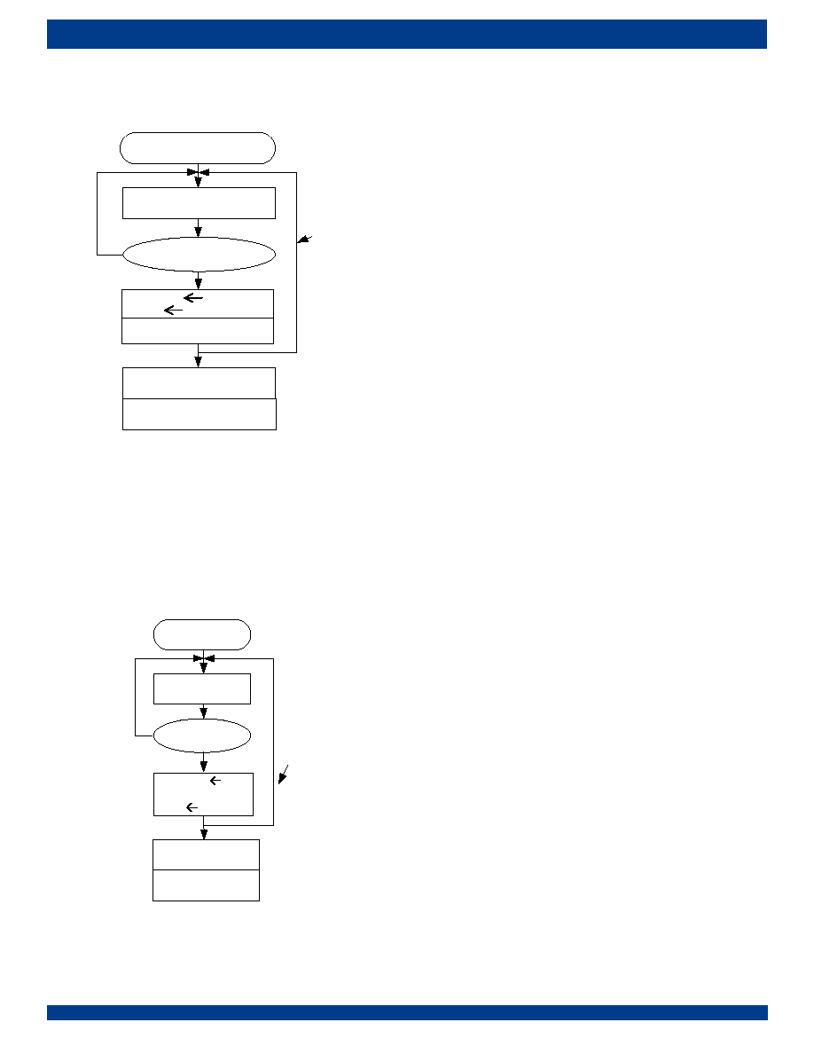
29
INDUSTRIAL
TEMPERATURE RANGES
QUAD CHANNEL T1/E1/J1 LONG HAUL/SHORT HAUL LINE INTERFACE UNIT
flows, a counter overflow interrupt which is indicated by CNT_OV_IS bit
(INTS1, 17H...) will be generated if it is not masked by CNT_IM bit (INTM1,
12H...).
Figure-17 Auto Report Mode
∑ Manual Report Mode
In Manual Report Mode, the internal Error Counter starts to count the
received errors when the CNT_MD bit (MAINT6, 10H...) is set to `0'. When
there is a `0' to `1' transition on the CNT_TRF bit (MAINT6, 10H...), the data
in the counter will be transferred to (CNT0, 18H...) and (CNT1, 19H...), then
the counter will be reset. The errors occurred during the transfer will be
accumulated to the next round. If the counter overflows, a counter overflow
interrupt indicated by CNT_OV_IS bit (INTS1, 17H...) will be generated if
it is not masked by CNT_IM bit (INTM1, 12H...).
Figure-18 Manual Report Mode
Note: 1. It is recommended that users should do the followings within next round
of error counting: Read the data in CNT0 and CNT1; Reset CNT_TRF bit
for the next `0' to `1' transition on this bit.
3.8.3
BIPOLAR VIOLATION AND PRBS ERROR INSERTION
Only when three consecutive `1's are detected in the transmit data
stream, will a `0' to `1' transition on the BPV_INS bit (MAINT6, 10H...) gen-
erate a bipolar violation pulse, and the polarity of the second `1' in the series
will be inverted.
A `0' to `1' transition on the EER_INS bit (MAINT6, 10H...)
will generate
a logic error during the PRBS/QRSS transmission.
3.9
LINE DRIVER FAILURE MONITORING
The transmit driver failure monitor can be enabled or disabled by setting
DFM_OFF bit (TCF1, 03H...). If the transmit driver failure monitor is
enabled, the transmit driver failure will be captured by DF_S bit (STAT0,
14H...). The transition of the DF_S bit is reflected by DF_IS bit (INTS0,
16H...), and, if enabled by DF_IM bit (INTM0, 11H...), will generate an inter-
rupt. When there is a short circuit on the TTIPn/TRINGn port, the output cur-
rent will be limited to 180 mA
PP
and an interrupt will be generated.
3.10 MCLK AND TCLK
3.10.1 MASTER CLOCK (MCLK)
MCLK is an independent, free-running reference clock. MCLK is 1.544
MHz or 37.056 MHz for T1/J1 applications and 2.048 MHz or 49.152 MHz
in E1 mode. This reference clock is used to generate several internal ref-
erence signals:
∑
Timing reference for the integrated clock recovery unit.
∑
Timing reference for the integrated digital jitter attenuator.
∑
Timing reference for microcontroller interface.
∑
Generation of RCLK signal during a loss of signal condition if AIS is
enabled.
∑
Reference clock during a blue alarm Transmit All Ones (TAOS), all
zeros, PRBS/QRSS and inband loopback patterns if it is selected
as the reference clock. For ATAO and AIS, MCLK is always used as
the reference clock.
Figure-19
shows the chip operation status in different conditions of
MCLK and TCLKn. The missing of MCLK will set all the four TTIP/TRING
to high impedance state.
3.10.2 TRANSMIT CLOCK (TCLK)
The TCLKn is used to sample the transmit data on TDn/TDPn, TDNn.
The active edge of TCLKn can be selected by the TCLK_SEL bit (TCF0,
02H...). During Transmit All Ones, PRBS/QRSS patterns or Inband Loop-
back Code, either TCLKn or MCLK can be used as the reference clock. This
is selected by the PATT_CLK bit (MAINT0, 0AH...).
But for Automatic Transmit All Ones and AIS, only MCLK is used as the
reference clock and the PATT_CLK bit is ignored. In Automatic Transmit
All Ones condition, the ATAO bit (MAINT0, 0AH) is set to `1'. In AIS condi-
tion, the AISE bit (MAINT0, 0AH) is set to `1'.
If TCLKn has been missing for more than 70 MCLK cycles, TCLK_LOS
bit (STAT0, 14H...) will be set, and the corresponding TTIPn/TRINGn will
become high impedance if this channel is not used for remote loopback or
is not using MCLK to transmit internal patterns (TAOS, All Zeros, PRBS and
in-band loopback code). When TCLKn is detected again, TCLK_LOS bit
(STAT0, 14H...) will be cleared. The reference frequency to detect a TCLKn
loss is derived from MCLK.
One-Second Timer expired?
counting
Auto Report Mode
(CNT_MD=1)
Bit TMOV_IS is set to '1'
Y
N
CNT0, CNT1 data in counter
counter 0
read the data in CNT0, CNT1 within
the next second
next second
repeats the
same process
Bit TMOV_IS is cleared after
the interrupt register is read
A '0' to '1' transition
on CNT_TRF?
counting
Manual Report mode
(CNT_MD=0)
CNT0, CNT1 data in
counter
counter 0
Y
N
next round
repeat the
same process
Read the data in CNT0,
CNT1 within next round
1
Reset CNT_TRF for the
next '0' to '1' transition

30
INDUSTRIAL
TEMPERATURE RANGES
QUAD CHANNEL T1/E1/J1 LONG HAUL/SHORT HAUL LINE INTERFACE UNIT
Figure-19 TCLK Operation Flowchart
3.11 MICROCONTROLLER INTERFACES
The microcontroller interface provides access to read and write the reg-
isters in the device. The chip supports serial processor interface and two
kinds of parallel processor interface: Motorola non_multiplexed mode and
Intel non_multiplexed mode. By pulling pin P/S to low or to High, the micro-
controller interface can be set to work in serial mode or in parallel mode
respectively. Refer to
7 MICROCONTROLLER INTERFACE TIMING
CHARACTERISTICS
for details.
3.11.1 PARALLEL MICROCONTROLLER INTERFACE
The interface is compatible with Motorola or Intel microcontroller. Pin
INT/MOT is used to select the operating mode of the parallel microcontroller
interface. When pin INT/MOT is pulled to Low, the parallel microcontroller
interface is configured for Motorola compatible hosts. When High, it is for
Intel compatible microcontrollers.
3.11.2 SERIAL MICROCONTROLLER INTERFACE
The serial interface pins include SCLK, SDI, SDO, CS as well as SCLKE
(control pin for the selection of serial clock active edge). By pulling P/S pin
to LOW, the device operates in the serial host Mode. In this mode, the reg-
isters are programmed through a 24-bit word which contains an 8-bit
address byte (A0~A7), a subsequent 8-bit command byte (bit R/W) and an
8-bit data byte (D0~D7). When bit R/W is `1', data is read out from pin SDO.
When bit R/W is `0', data is written into SDI pin. Refer to
Figure-20
.
Figure-20 Serial Processor Interface Function Timing
3.12 INTERRUPT HANDLING
All kinds of interrupt of the IDT82V2084 are indicated by the INT pin.
When the INT_PIN[0] bit (GCF0, 40H) is `0', the INT pin is open drain active
low, with a 10 K
external pull-up resistor. When the INT_PIN[1:0] bits
(GCF0, 40H) are `01', the INT pin is push-pull active low; when the
INT_PIN[1:0] bits are `10', the INT pin is push-pull active high.
All the interrupt can be disabled by the INTM_GLB bit (GCF0, 40H).
When the INTM_GLB bit (GCF0, 40H) is set to `0', an active level on the
INT pin represents an interrupt of the IDT82V2084. The INT_CH[7:0] bits
(INTCH, 80H) should be read to identify which channel(s) generate the
interrupt.
The interrupt event is captured by the corresponding bit in the Interrupt
Status Register (INTS0, 16H...) or (INTS1, 17H...). Every kind of interrupt
can be enabled/disabled individually by the corresponding bit in the register
normal operation mode
transmitter n enters high
impedance status and
generates transmit clock loss
interrupt if not masked
TCLKn status?
clocked
L/H
MCLK=H/L?
all transmitters high
impedance status
yes
clocked
A0
A1
A2
A3
A4
A5
A6
A7
R/W
D0
D1
D2
D3
D4
D5
D6
D7
CS
SCLK
SDI
address byte
command byte
input data byte (R/W=0)
D0
D1
D2
D3
D4
D5
D6
D7
remains high impedance
SDO
Output data byte (R/W=1)
D o n ' t C a r e

31
INDUSTRIAL
TEMPERATURE RANGES
QUAD CHANNEL T1/E1/J1 LONG HAUL/SHORT HAUL LINE INTERFACE UNIT
(INTM0, 11H...) or (INTM1, 12H...). Some event is reflected by the corre-
sponding bit in the Status Register (STAT0, 14H...) or (STAT1, 15H...), and
the Interrupt Trigger Edge Selection Register can be used to determine how
the Status Register sets the Interrupt Status Register.
After the Interrupt Status Register (INTS0, 16H...) or (INTS1, 17H...) is
read, the corresponding bit indicating which channel generates the inter-
rupt in the INTCH register (80H) will be reset. Only when all the pending
interrupt is acknowledged through reading the Interrupt Status Registers
of all the channels (INTS0, 16H...) or (INTS1, 17H...) will all the bits in the
INTCH register (80H) be reset and the INT pin become inactive.
There are totally fourteen kinds of events that could be the interrupt
source for one channel:
(1).LOS Detected
(2).AIS Detected
(3).Driver Failure Detected
(4).TCLK Loss
(5).Synchronization Status of PRBS
(6).PRBS Error Detected
(7).Code Violation Received
(8).Excessive Zeros Received
(9).JA FIFO Overflow/Underflow
(10).Inband Loopback Code Status
(11).Equalizer Out of Range
(12).One-Second Timer Expired
(13).Error Counter Overflow
(14).Arbitrary Waveform Generator Overflow
Table-22
is a summary of all kinds of interrupt and their associated Sta-
tus bit, Interrupt Status bit, Interrupt Trigger Edge Selection bit and Interrupt
Mask bit.
3.13 5V TOLERANT I/O PINS
All digital input pins will tolerate 5.0
±
5% volts and are compatible with
TTL logic.
3.14 RESET OPERATION
The chip can be reset in two ways:
∑
Software Reset: Writing to the RST register (20H) will reset the chip
in 1 us.
∑
Hardware Reset: Asserting the RST pin low for a minimum of 100 ns
will reset the chip.
After reset, all drivers output are in high impedance state, all the internal
flip-flops are reset, and all the registers are initialized to default values.
3.15 POWER SUPPLY
This chip uses a single 3.3 V power supply.
Table-22 Interrupt Event
Interrupt Event
Status bit
(STAT0, STAT1)
Interrupt Status bit
(INTS0, INTS1)
Interrupt Edge Selection bit
(INTES)
Interrupt Mask bit
(INTM0, INTM1)
LOS Detected
LOS_S
LOS_IS
LOS_IES
LOS_IM
AIS Detected
AIS_S
AIS_IS
AIS_IES
AIS_IM
Driver Failure Detected
DF_S
DF_IS
DF_IES
DF_IM
TCLKn Loss
TCLK_LOS
TCLK_LOS_IS
TCLK_IES
TCLK_IM
Synchronization Status of PRBS/QRSS
PRBS_S
PRBS_IS
PRBS_IES
PRBS_IM
PRBS/QRSS Error
ERR_IS
ERR_IM
Code Violation Received
CV_IS
CV_IM
Excessive Zeros Received
EXZ_IS
EXZ_IM
JA FIFO Overflow
JAOV_IS
JAOV_IM
JA FIFO Underflow
JAUD_IS
JAUD_IM
Equalizer Out of Range
EQ_S
EQ_IS
EQ_IES
EQ_IM
Inband Loopback Activate Code Status
IBLBA_S
IBLBA_IS
IBLBA_IES
IBLBA_IM
Inband Loopback Deactivate Code Status
IBLBD_S
IBLBD_IS
IBLBD_IES
IBLBD_IM
One-Second Timer Expired
TMOV_IS
TIMER_IM
Error Counter Overflow
CNT_OV_IS
CNT_IM
Arbitrary Waveform Generator Overflow
DAC_OV_IS
DAC_OV_IM
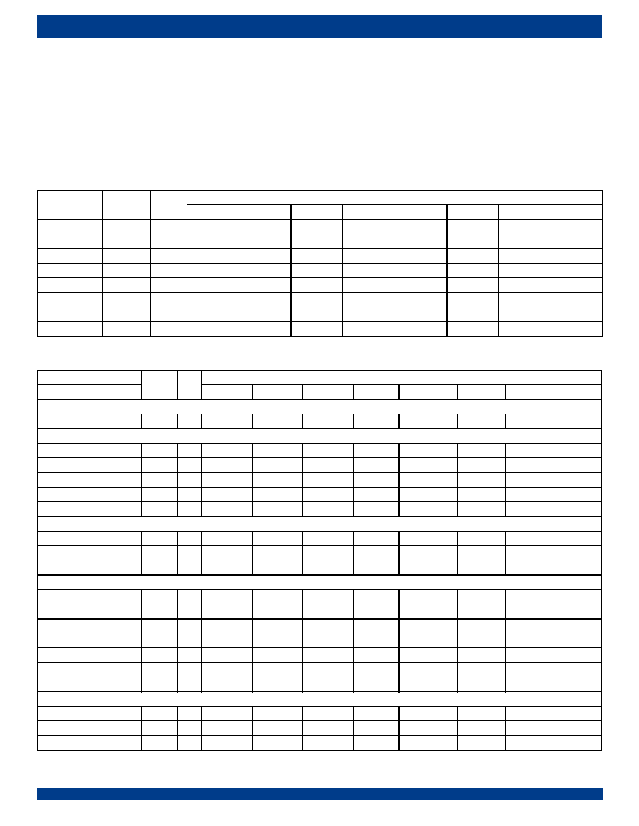
32
INDUSTRIAL
TEMPERATURE RANGES
QUAD CHANNEL T1/E1/J1 LONG HAUL/SHORT HAUL LINE INTERFACE UNIT
4
PROGRAMMING INFORMATION
4.1
REGISTER LIST AND MAP
The IDT82V2084 registers can be divided into Global Registers and
Local Registers. The operation on the Global Registers affects all the four
channels while the operation on Local Registers only affects that specific
channel. For different channel, the address of Local Register is different.
Table-23
is the map of Global Registers and
Table-24
is the map of Local
Registers. If the configuration of all the four channels is the same, the COPY
bit (GCF0, 40H) can be set to `1' to establish the Broadcasting mode. In the
Broadcasting mode, the Writing operation on any of the four channels' reg-
isters will be copied to the corresponding registers of all the other channels.
Table-23 Global Register List and Map
Address (Hex)
Register
R/W
Map
b7
b6 b5 b4 b3 b2
b1
b0
00 ID
R
ID7
ID6
ID5
ID4
ID3
ID2
ID1
ID0
20
RST
W
40
GCF0
R/W
-
-
-
T1E1
COPY
INTM_GLB
INT_PIN1
INT_PIN0
60
GCF1
R/W
MON3
MON2
MON1
MON0
-
-
-
-
80
INTCH
R
-
INT_CH4
-
INT_CH3
-
INT_CH2
-
INT_CH1
A0
Reserved
C0 Reserved
E0 Reserved
Table-24 Per Channel Register List and Map
Address (Hex)
Register R/W
Map
CH1-CH4
b7
b6 b5 b4 b3 b2
b1
b0
Jitter Attenuation Control Register
01,41,81,C1
JACF
R/W
-
-
JA_LIMIT
JACF1
JACF0
JADP1
JADP0
JABW
Transmit Path Control Registers
02,42,82,C2
TCF0
R/W
-
-
-
T_OFF
TD_INV
TCLK_SEL
T_MD1
T_MD0
03,43,83,C3
TCF1
R/W
-
-
DFM_OFF
THZ
PULS3
PULS2
PULS1
PULS0
04,44,84,C4
TCF2
R/W
-
-
SCAL5
SCAL4
SCAL3
SCAL2
SCAL1
SCAL0
05,45,85,C5
TCF3
R/W
DONE
RW
UI1
UI0
SAMP3
SAMP2
SAMP1
SAMP0
06,46,86,C6
TCF4
R/W
-
WDAT6
WDAT5
WDAT4
WDAT3
WDAT2
WDAT1
WDAT0
Receive Path Control Registers
07,47,87,C7
RCF0
R/W
-
-
- R_OFF
RD_INV
RCLK_SEL
R_MD1
R_MD0
08,48,88,C8
RCF1
R/W
-
EQ_ON
-
LOS4
LOS3
LOS2
LOS1
LOS0
09,49,89,C9
RCF2
R/W
-
-
SLICE1
SLICE0 UPDW1
UPDW0
MG1
MG0
Network Diagnostics Control Registers
0A,4A,8A,CA
MAINT0 R/W
-
PATT1
PATT0
PATT_CLK
PRBS_INV
LAC
AISE
ATAO
0B,4B,8B,CB
MAINT1
-
-
-
-
ARLP
RLP
ALP
DLP
0C,4C,8C,CC
MAINT2 R/W
-
-
TIBLB_L1
TIBLB_L0 RIBLBA_L1
RIBLBA_L0 RIBLBD_L1 RIBLBD_L0
0D,4D,8D,CD
MAINT3 R/W
TIBLB7
TIBLB6
TIBLB5
TIBLB4
TIBLB3
TIBLB2
TIBLB1
TIBLB0
0E,4E,8E,CE
MAINT4 R/W
RIBLBA7
RIBLBA6
RIBLBA5
RIBLBA4
RIBLBA3
RIBLBA2
RIBLBA1
RIBLBA0
0F,4F,8F,CF
MAINT5 R/W
RIBLBD7
RIBLBD6
RIBLBD5
RIBLBD4
RIBLBD3
RIBLBD2
RIBLBD1
RIBLBD0
10,50,90,D0
MAINT6 R/W
-
BPV_INS
ERR_INS
EXZ_DEF
ERR_SEL1
ERR_SEL0
CNT_MD
CNT_TRF
Interrupt Control Registers
11,51,91,D1
INTM0
R/W
EQ_IM
IBLBA_IM
IBLBD_IM
PRBS_IM
TCLK_IM
DF_IM
AIS_IM
LOS_IM
12,52,92,D2
INTM1
R/W DAC_OV_IM
JAOV_IM
JAUD_IM
ERR_IM
EXZ_IM
CV_IM
TIMER_IM
CNT_IM
13,53,93,D3
INTES
R/W
EQ_IES
IBLBA_IES
IBLBD_IES PRBS_IES
TCLK_IES
DF_IES
AIS_IES
LOS_IES

33
INDUSTRIAL
TEMPERATURE RANGES
QUAD CHANNEL T1/E1/J1 LONG HAUL/SHORT HAUL LINE INTERFACE UNIT
4.2
REGISTER DESCRIPTION
4.2.1
GLOBAL REGISTERS
Line Status Registers
14,54,94,D4
STAT0
R
EQ_S
IBLBA_S
IBLBD_S
PRBS_S
TCLK_LOS
DF_S
AIS_S
LOS_S
15,55,95,D5
STAT1
R
-
-
RLP_S
LATT4
LATT3
LATT2
LATT1
LATT0
Interrupt Status Registers
16,56,96,D6
INTS0
R
EQ_IS
IBLBA_IS
IBLBD_IS
PRBS_IS TCLK_LOS_IS
DF_IS
AIS_IS
LOS_IS
17,57,97,D7
INTS1
R
DAC_OV_IS
JAOV_IS
JAUD_IS
ERR_IS
EXZ_IS
CV_IS
TMOV_IS CNT_OV_IS
Counter Registers
18,58,98,D8
CNT0
R
Bit7
Bit6
Bit5
Bit4
Bit3
Bit2
Bit1
Bit0
19,59,99,D9
CNT1
R
Bit15
Bit14
Bit13
Bit12
Bit11
Bit10
Bit9
Bit8
Transmit and Receive Termination Registers
1A,5A,9A,DA
TERM
R/W
-
-
T_TERM2
T_TERM1
T_TERM0 R_TERM2
R_TERM1
R_TERM0
Table-24 Per Channel Register List and Map (Continued)
Address (Hex)
Register R/W
Map
CH1-CH4
b7
b6 b5 b4 b3 b2
b1
b0
Table-25 ID: Device Revision Register
(R, Address = 00H)
Symbol
Bit
Default
Description
ID[7:0]
7-0
00H
An 8-bit word is pre-set into the device as the revision number. This number is different from the functional
changes and is mask programmed
Table-26 RST: Reset Register
(W, Address = 20H)
Symbol
Bit
Default
Description
RST[7:0]
7-0
00H
Software reset. A write operation on this register will reset all internal registers to their default values, and the sta-
tus of all ports are set to the default status. The content in this register can not be changed.
Table-27 GCF0: Global Configuration Register 0
(R/W, Address = 40H)
Symbol
Bit
Default
Description
-
7-6
0
Reserved
-
5
0
Reserved. For normal operation, this bit should be set to `0'.
T1E1
4
0
This bit selects E1 or T1/J1 operation mode globally.
= 0: E1 mode is selected.
= 1: T1/J1 mode is selected.
COPY
3
0
Enable broadcasting mode.
= 0: Broadcasting mode disabled
= 1: Broadcasting mode enabled. Writing operation on one channel's register will be copied exactly to the corre-
sponding registers in all the other channels.
INTM_GLB
2
1
Global interrupt enable
= 0: Interrupt is globally enabled. But for each individual interrupt, it still can be disabled by its corresponding Inter-
rupt mask Bit.
= 1: All the interrupts are disabled for all channels.
INT_PIN[1:0]
1-0
00
Interrupt pin operation mode selection
= x0: open drain, active low (with an external pull-up resistor)
= 01: push-pull, active low
= 11: push-pull, active high

34
INDUSTRIAL
TEMPERATURE RANGES
QUAD CHANNEL T1/E1/J1 LONG HAUL/SHORT HAUL LINE INTERFACE UNIT
4.2.2
JITTER ATTENUATION CONTROL REGISTER
Table-28 GCF1: Global Configuration Register 1
(R/W, Address = 60H)
Symbol
Bit
Default
Description
MON[3:0]
7-4
0000
MON selects the transmitter or receiver channel to be monitored.
= 0000: receiver 1 is in normal operation without monitoring
= 0001: reserved
= 0010: monitor receiver 2
= 0011: reserved
= 0100: monitor receiver 3
= 0101: reserved
= 0110: monitor receiver 4
= 0111: reserved
= 1000: transmitter 1 is in normal operation without monitoring
= 1001: reserved
= 1010: monitor transmitter 2
= 1011: reserved
= 1100: monitor transmitter 3
= 1101: reserved
= 1110: monitor transmitter 4
= 1111: reserved
-
3-0
0000
Reserved
Table-29 INTCH: Interrupt Channel Indication Register
(R, Address = 80H)
Symbol
Bit
Default
Description
INT_CH[7:0]
7-0
00H
INT_CH[0, 2, 4 or 6]=1 indicates that an interrupt was generated by channel 1, 2, 3 or 4 respectively.
Table-30 JACF: Jitter Attenuator Configuration Register
(R/W, Address = 01H,41H,81H,C1H)
Symbol
Bit
Default
Description
-
7-6
00
Reserved
JA_LIMIT
5
0
Wide Jitter Attenuation bandwidth
= 0: normal mode
= 1: JA limit mode
JACF[1:0]
4-3
00
Jitter Attenuator configuration
= 00/10: JA not used
= 01: JA in transmit path
= 11: JA in receive path
JADP[1:0]
2-1
00
Jitter Attenuator depth selection
= 00: 128 bits
= 01: 64 bits
= 10/11: 32 bits
JABW
0
0
Jitter transfer function bandwidth selection
JABW
T1/J1
E1
0
5 Hz
6.8 Hz
1
1.25 Hz
0.9 Hz

35
INDUSTRIAL
TEMPERATURE RANGES
QUAD CHANNEL T1/E1/J1 LONG HAUL/SHORT HAUL LINE INTERFACE UNIT
4.2.3
TRANSMIT PATH CONTROL REGISTERS
1. In internal impedance matching mode, for E1/75
cable impedance, the PULS[3:0] bits (TCF1, 03H...) should be set to `0000'. In external impedance matching
mode, for E1/75
cable impedance, the PULS[3:0] bits should be set to `0001'.
Table-31 TCF0: Transmitter Configuration Register 0
(R/W, Address = 02H,42H,82H,C2H)
Symbol
Bit
Default
Description
-
7-5
000
Reserved
T_OFF
4
0
Transmitter power down enable
= 0: Transmitter power up
= 1: Transmitter power down and line driver high impedance
TD_INV
3
0
Transmit data invert
= 0: data on TDn or TDPn/TDNn is active high
= 1: data on TDn or TDPn/TDNn is active low
TCLK_SEL
2
0
Transmit clock edge select
= 0: data on TDn or TDPn/TDNn is sampled on the falling edges of TCLKn
= 1: data on TDn or TDPn/TDNn is sampled on the rising edges of TCLKn
T_MD[1:0]
1-0
00
Transmitter operation mode control bits which select different stages of transmit data path
= 00: enable HDB3/B8ZS encoder and waveform shaper blocks, input on TDn is single rail NRZ data
= 01: enable AMI encoder and waveform shaper blocks, input on pin TDn is single rail NRZ data
= 1x: encoder is bypassed, dual rail NRZ transmit data input on pin TDPn/TDNn
Table-32 TCF1: Transmitter Configuration Register 1
(R/W, Address = 03H,43H,83H,C3H)
Symbol
Bit
Default
Description
-
7-6
00
Reserved. This bit should be `0' for normal operation.
DFM_OFF
5
0
Transmit driver failure monitor disable
= 0: DFM is enabled
= 1: DFM is disabled
THZ
4
1
Transmit line driver tri-state enable
= 0: normal state
= 1: transmit line driver tri-state (other transmit path still in normal state)
PULS[3:0]
3-0
0000
These bits select the transmit template/LBO for short-haul/long-haul applications.
T1/E1/J1
TCLK
Cable
Impedance
Cable Range
or LBO
Cable Loss
0000
1
E1
2.048 MHz
75
-
0~43 dB (default)
0001
E1
2.048 MHz
120
-
0~43 dB
0010
DSX1
1.544 MHz
100
0~133 ft
0~0.6 dB
0011
DSX1
1.544 MHz
100
133~266 ft
0.6~1.2 dB
0100
DSX1
1.544 MHz
100
266~399 ft
1.2~1.8 dB
0101
DSX1
1.544 MHz
100
399~533 ft
1.8~2.4 dB
0110
DSX1
1.544 MHz
100
533~655 ft
2.4~3.0 dB
0111
J1
1.544 MHz
110
0~655 ft
0~3.0 dB
1000
DS1
1.544 MHz
100
0 dB LBO
0~36 dB
1001
DS1
1.544 MHz
100
-7.5 dB LBO
0~28.5 dB
1010
DS1
1.544 MHz
100
-15 dB LBO
0~21 dB
1011
DS1
1.544 MHz
100
-22.5 dB LBO
0~13.5 dB
11xx
User programmable waveform setting

36
INDUSTRIAL
TEMPERATURE RANGES
QUAD CHANNEL T1/E1/J1 LONG HAUL/SHORT HAUL LINE INTERFACE UNIT
Table-33 TCF2: Transmitter Configuration Register 2
(R/W, Address = 04H,44H,84H,C4H)
Symbol
Bit
Default
Description
-
7-6
00
Reserved
SCAL[5:0]
5-0
100001
SCAL specifies a scaling factor to be applied to the amplitude of the user-programmable arbitrary pulses which is
to be transmitted if needed. The default value of SCAL[5:0] is `100001'. Refer to
3.2.3.3 User-Programmable Arbi-
trary Waveform
.
= 110110: default value for T1 0~133 ft, T1 133~266 ft, T1 266~399 ft, T1 399~533 ft, T1 533~655 ft, J1 0~655 ft,
DS1 0dB LBO. One step change of this value results in 2% scaling up/down against the pulse amplitude.
= 010001: default value for DS1 -7.5 dB LBO. One step change of this value results in 6.25% scaling up/down
against the pulse amplitude.
= 001000: default value for DS1 -15.0 dB LBO. One step change of this value results in 12.5% scaling up/down
against the pulse amplitude.
= 000100: default value for DS1 -22.5 dB LBO. One step change of this value results in 25% scaling up/down
against the pulse amplitude.
= 100001: default value for E1 75
and 120 . One step change of this value results in 3% scaling up/down
against the pulse amplitude.
Table-34 TCF3: Transmitter Configuration Register 3
(R/W, Address = 05H,45H,85H,C5H)
Symbol
Bit
Default
Description
DONE
7
0
After `1' is written to this bit, a read or write operation is implemented.
RW
6
0
This bit selects read or write operation
= 0: write to RAM
= 1: read from RAM
UI[1:0]
5-4
00
These bits specify the unit interval address. There are 4 unit intervals.
= 00: UI address is 0 (The most left UI)
= 01: UI address is 1
= 10: UI address is 2
= 11: UI address is 3
SAMP[3:0]
3-0
0000
These bits specify the sample address. Each UI has 16 samples.
= 0000: sample address is 0 (The most left Sample)
= 0001: sample address is 1
= 0010: sample address is 2
......
= 1110: sample address is 14
= 1111: sample address is 15
Table-35 TCF4: Transmitter Configuration Register 4
(R/W, Address = 06H,46H,86H,C6H)
Symbol
Bit
Default
Description
-
7
0
Reserved
WDAT[6:0]
6-0
0000000
In Indirect Write operation, the WDAT[6:0] will be loaded to the pulse template RAM, specifying the amplitude of
the Sample.
After an Indirect Read operation, the amplitude data of the Sample in the pulse template RAM will be output to the
WDAT[6:0].

37
INDUSTRIAL
TEMPERATURE RANGES
QUAD CHANNEL T1/E1/J1 LONG HAUL/SHORT HAUL LINE INTERFACE UNIT
4.2.4
RECEIVE PATH CONTROL REGISTERS
Table-36 RCF0: Receiver Configuration Register 0
(R/W, Address = 07H,47H,87H,C7H)
Symbol
Bit
Default
Description
-
7-5
000
Reserved
R_OFF
4
0
Receiver power down enable
= 0: Receiver power up
= 1: Receiver power down
RD_INV
3
0
Receive data invert
= 0: data on RDn or RDPn/RDNn is active high
= 1: data on RDn or RDPn/RDNn is active low
RCLK_SEL
2
0
Receive clock edge select (this bit is ignored in slicer mode)
= 0: data on RDn or RDPn/RDNn is updated on the rising edges of RCLKn
= 1: data on RDn or RDPn/RDNn is updated on the falling edges of RCLKn
R_MD[1:0]
1-0
00
Receiver path decoding selection
= 00: receive data is HDB3 (E1) / B8ZS (T1/J1) decoded and output on RDn with single rail NRZ format
= 01: receive data is AMI decoded and output on RDn with single rail NRZ format
= 10: decoder is bypassed, re-timed dual rail data with NRZ format output on RDPn/RDNn (dual rail mode with
clock recovery)
= 11: both CDR and decoder blocks are bypassed, slicer data with RZ format output on RDPn/RDNn (slicer
mode)

38
INDUSTRIAL
TEMPERATURE RANGES
QUAD CHANNEL T1/E1/J1 LONG HAUL/SHORT HAUL LINE INTERFACE UNIT
Table-37 RCF1: Receiver Configuration Register 1
(R/W, Address = 08H,48H,88H,C8H)
Symbol
Bit
Default
Description
-
7
0
Reserved
EQ_ON
6
0
= 0: receive equalizer off (short haul receiver)
= 1: receive equalizer on (long haul receiver)
-
5
0
Reserved. Should be 0 for normal operation.
LOS[4:0]
4-0
10101
LOS Clear Level (dB)
LOS Declare Level (dB)
00000
0
<-4
00001
>-2
<-6
00010
>-4
<-8
00011
>-6
<-10
00100
>-8
<-12
00101
>-10
<-14
00110
>-12
<-16
00111
>-14
<-18
01000
>-16
<-20
01001
>-18
<-22
01010
>-20
<-24
01011
>-22
<-26
01100
>-24
<-28
01101
>-26
<-30
01110
>-28
<-32
01111
>-30
<-34
10000
>-32
<-36
10001
>-34
<-38
10010
>-36
<-40
10011
>-38
<-42
10100
>-40
<-44
10101
>-42
<-46
10110-11111
>-44
<-48

39
INDUSTRIAL
TEMPERATURE RANGES
QUAD CHANNEL T1/E1/J1 LONG HAUL/SHORT HAUL LINE INTERFACE UNIT
4.2.5
NETWORK DIAGNOSTICS CONTROL REGISTERS
Table-38 RCF2: Receiver Configuration Register 2
(R/W, Address =09H,49H,89H,C9H)
Symbol
Bit
Default
Description
-
7-6
00
Reserved
SLICE[1:0]
5-4
01
Receive slicer threshold
= 00: The receive slicer generates a mark if the voltage on RTIPn/RRINGn exceeds 40% of the peak amplitude.
= 01: The receive slicer generates a mark if the voltage on RTIPn/RRINGn exceeds 50% of the peak amplitude.
= 10: The receive slicer generates a mark if the voltage on RTIPn/RRINGn exceeds 60% of the peak amplitude.
= 11: The receive slicer generates a mark if the voltage on RTIPn/RRINGn exceeds 70% of the peak amplitude.
UPDW[1:0]
3-2
10
Equalizer observation window
= 00: 32 bits
= 01: 64 bits
= 10: 128 bits
= 11: 256 bits
MG[1:0]
1-0
00
Monitor gain setting: these bits select the internal linear gain boost
= 00: 0 dB
= 01: 22 dB
= 10: 26 dB
= 11: 32 dB
Table-39 MAINT0: Maintenance Function Control Register 0
(R/W, Address = 0AH,4AH,8AH,CAH)
Symbol
Bit
Default
Description
-
7
0
Reserved
PATT[1:0]
6-5
00
These bits select the internal pattern and insert it into the transmit data stream.
= 00: normal operation (PATT_CLK = 0) / insert all zeros (PATT_CLK = 1)
= 01: insert All Ones
= 10: insert PRBS (E1: 2
15
-1) or QRSS (T1/J1: 2
20
-1)
= 11: insert programmable Inband Loopback activate or deactivate code
PATT_CLK
4
0
Selects reference clock for transmitting internal pattern
= 0: uses TCLKn as the reference clock
= 1: uses MCLK as the reference clock
PRBS_INV
3
0
Inverts PRBS
= 0: PRBS data is not inverted
= 1: PRBS data is inverted before transmission and detection
LAC
2
0
The LOS/AIS criterion is selected as below:
= 0: G.775 (E1) / T1.231 (T1/J1)
= 1: ETSI 300233 & I.431 (E1) / I.431 (T1/J1)
AISE
1
0
AIS enable during LOS
= 0: AIS insertion on RDPn/RDNn/RCLKn is disabled during LOS
= 1: AIS insertion on RDPn/RDNn/RCLKn is enabled during LOS
ATAO
0
0
Automatically Transmit All Ones (enabled only when PATT[1:0] = 01)
= 0: disabled
= 1: Automatically Transmit All Ones pattern at TTIPn/TRINGn during LOS.

40
INDUSTRIAL
TEMPERATURE RANGES
QUAD CHANNEL T1/E1/J1 LONG HAUL/SHORT HAUL LINE INTERFACE UNIT
Table-40 MAINT1: Maintenance Function Control Register 1
(R/W, Address = 0BH,4BH,8BH,CBH)
Symbol
Bit
Default
Description
-
7-4
0000
Reserved
ARLP
3
0
Automatic Remote Loopback Control
= 0: disables Automatic Remote Loopback (normal transmit and receive operation)
= 1: enables Automatic Remote Loopback
RLP
2
0
Remote loopback enable
= 0: disables remote loopback (normal transmit and receive operation)
= 1: enables remote loopback
ALP
1
0
Analog loopback enable
= 0: disables analog loopback (normal transmit and receive operation)
= 1: enables analog loopback
DLP
0
0
Digital loopback enable
= 0: disables digital loopback (normal transmit and receive operation)
= 1: enables digital loopback
Table-41 MAINT2: Maintenance Function Control Register 2
(R/W, Address = 0CH,4CH,8CH,CCH)
Symbol
Bit
Default
Description
-
7-6
00
Reserved.
TIBLB_L[1:0]
5-4
00
Defines the length of the user-programmable transmit Inband Loopback activate/deactivate code contained in
TIBLB register. The default selection is 5 bits length.
= 00: 5-bit activate code in TIBLB [4:0]
= 01: 6-bit activate code in TIBLB [5:0]
= 10: 7-bit activate code in TIBLB [6:0]
= 11: 8-bit activate code in TIBLB [7:0]
RIBLBA_L[1:0]
3-2
00
Defines the length of the user-programmable receive Inband Loopback activate code contained in RIBLBA regis-
ter.
= 00: 5-bit activate code in RIBLBA [4:0]
= 01: 6-bit activate code in RIBLBA [5:0]
= 10: 7-bit activate code in RIBLBA [6:0]
= 11: 8-bit activate code in RIBLBA [7:0]
RIBLBD_L[1:0]
1-0
01
Defines the length of the user-programmable receive Inband Loopback deactivate code contained in RIBLBD reg-
ister.
= 00: 5-bit deactivate code in RIBLBD [4:0]
= 01: 6-bit deactivate code in RIBLBD [5:0]
= 10: 7-bit deactivate code in RIBLBD [6:0]
= 11: 8-bit deactivate code in RIBLBD [7:0]
Table-42 MAINT3: Maintenance Function Control Register 3
(R/W, Address = 0DH,4DH,8DH,CDH)
Symbol
Bit
Default
Description
TIBLB[7:0]
7-0
(000)00001 Defines the user-programmable transmit Inband Loopback activate/deactivate code. The default selection is
00001.
TIBLB[7:0] form the 8-bit repeating code
TIBLB[6:0] form the 7-bit repeating code
TIBLB[5:0] form the 6-bit repeating code
TIBLB[4:0] form the 5-bit repeating code

41
INDUSTRIAL
TEMPERATURE RANGES
QUAD CHANNEL T1/E1/J1 LONG HAUL/SHORT HAUL LINE INTERFACE UNIT
Table-43 MAINT4: Maintenance Function Control Register 4
(R/W, Address = 0EH,4EH,8EH,CEH)
Symbol
Bit
Default
Description
RIBLBA[7:0]
7-0
(000)00001 Defines the user-programmable receive Inband Loopback activate code. The default selection is 00001.
RIBLBA[7:0] form the 8-bit repeating code
RIBLBA[6:0] form the 7-bit repeating code
RIBLBA[5:0] form the 6-bit repeating code
RIBLBA[4:0] form the 5-bit repeating code
Table-44 MAINT5: Maintenance Function Control Register 5
(R/W, Address = 0FH,4FH,8FH,CFH)
Symbol
Bit
Default
Description
RIBLBD[7:0]
7-0
(00)001001 Defines the user-programmable receive Inband Loopback deactivate code. The default selection is 001001.
RIBLBD[7:0] form the 8-bit repeating code
RIBLBD[6:0] form the 7-bit repeating code
RIBLBD[5:0] form the 6-bit repeating code
RIBLBD[4:0] form the 5-bit repeating code
Table-45 MAINT6: Maintenance Function Control Register 6
(R/W, Address = 10H,50H,90H,D0H)
Symbol
Bit
Default
Description
-
7
0
Reserved.
BPV_INS
6
0 BPV
error
insertion
A `0' to `1' transition on this bit will cause a single bipolar violation error to be inserted into the transmit data
stream. This bit must be cleared and set again for a subsequent error to be inserted.
ERR_INS
5
0
PRBS/QRSS logic error insertion
A `0' to `1' transition on this bit will cause a single PRBS/QRSS logic error to be inserted into the transmit PRBS/
QRSS data stream. This bit must be cleared and set again for subsequent error to be inserted.
EXZ_DEF
4
0
EXZ definition select
= 0: ANSI
= 1: FCC
ERR_SEL
3-2
00
These bits choose which type of error will be counted
= 00: the PRBS logic error is counted by a 16-bit error counter.
= 01: the EXZ error is counted by a 16-bit error counter.
= 10: the Received CV (BPV) error is counted by a 16-bit error counter.
= 11: do not detect and count the receiver error.
CNT_MD
1
0
Counter operation mode select
= 0: Manual Report Mode
= 1: Auto Report Mode
CNT_TRF
0
0
= 0: Clear this bit for the next `0' to `1' transition on this bit.
= 1: Error counting result is transferred to CNT0 and CNT1 and the error counter is reset.

42
INDUSTRIAL
TEMPERATURE RANGES
QUAD CHANNEL T1/E1/J1 LONG HAUL/SHORT HAUL LINE INTERFACE UNIT
4.2.6
INTERRUPT CONTROL REGISTERS
Table-46 INTM0: Interrupt Mask Register 0
(R/W, Address = 11H,51H,91H,D1H)
Symbol
Bit
Default
Description
EQ_IM
7
1
Equalizer out of range interrupt mask
= 0: Equalizer out of range interrupt enabled
= 1: Equalizer out of range interrupt masked
IBLBA_IM
6
1
In-band Loopback activate code detect interrupt mask
= 0: In-band Loopback activate code detect interrupt enabled
= 1: In-band Loopback activate code detect interrupt masked
IBLBD_IM
5
1
In-band Loopback deactivate code detect interrupt mask
= 0: In-band Loopback deactivate code detect interrupt enabled
= 1: In-band Loopback deactivate code detect interrupt masked
PRBS_IM
4
1
PRBS synchronic signal detect interrupt mask
= 0: PRBS synchronic signal detect interrupt enabled
= 1: PRBS synchronic signal detect interrupt masked
TCLK_IM
3
1
TCLK loss detect interrupt mask
= 0: TCLK loss detect interrupt enabled
= 1: TCLK loss detect interrupt masked
DF_IM
2
1
Driver failure interrupt mask
= 0: Driver failure interrupt enabled
= 1: Driver failure interrupt masked
AIS_IM
1
1
Alarm Indication Signal interrupt mask
= 0: Alarm Indication Signal interrupt enabled
= 1: Alarm Indication Signal interrupt masked
LOS_IM
0
1
Loss Of Signal interrupt mask
= 0: Loss Of Signal interrupt enabled
= 1: Loss Of Signal interrupt masked

43
INDUSTRIAL
TEMPERATURE RANGES
QUAD CHANNEL T1/E1/J1 LONG HAUL/SHORT HAUL LINE INTERFACE UNIT
Table-47 INTM1: Interrupt Mask Register 1
(R/W, Address = 12H,52H,92H,D2H)
Symbol
Bit
Default
Description
DAC_OV_IM
7
1
DAC arithmetic overflow interrupt mask
= 0: DAC arithmetic overflow interrupt enabled
= 1: DAC arithmetic overflow interrupt masked
JAOV_IM
6
1
JA overflow interrupt mask
= 0: JA overflow interrupt enabled
= 1: JA overflow interrupt masked
JAUD_IM
5
1
JA underflow interrupt mask
= 0: JA underflow interrupt enabled
= 1: JA underflow interrupt masked
ERR_IM
4
1
PRBS/QRSS logic error detect interrupt mask
= 0: PRBS/QRSS logic error detect interrupt enabled
= 1: PRBS/QRSS logic error detect interrupt masked
EXZ_IM
3
1
Receive excess zeros interrupt mask
= 0: Receive excess zeros interrupt enabled
= 1: Receive excess zeros interrupt masked
CV_IM
2
1
Receive error interrupt mask
= 0: Receive error interrupt enabled
= 1: Receive error interrupt masked
TIMER_IM
1
1
One-Second Timer expiration interrupt mask
= 0: One-Second Timer expiration interrupt enabled
= 1: One-Second Timer expiration interrupt masked
CNT_IM
0
1
Counter overflow interrupt mask
= 0: Counter overflow interrupt enabled
= 1: Counter overflow interrupt masked

44
INDUSTRIAL
TEMPERATURE RANGES
QUAD CHANNEL T1/E1/J1 LONG HAUL/SHORT HAUL LINE INTERFACE UNIT
Table-48 INTES: Interrupt Trigger Edges Select Register
(R/W, Address = 13H, 53H,93H,D3H)
Symbol
Bit
Default
Description
EQ_IES
7
0
This bit determines the Equalizer out of range interrupt event.
= 0: interrupt event is defined as a `0' to `1' transition of the EQ_S bit in the STAT0 status register
= 1: interrupt event is defined as either a `0' to `1' transition or a `1' to `0' transition of the EQ_S bit in the STAT0
status register.
IBLBA_IES
6
0
This bit determines the Inband Loopback Activate Code interrupt event.
= 0: interrupt event is defined as a `0' to `1' transition of the IBLBA_S bit in the STAT0 status register
= 1: interrupt event is defined as either a `0' to `1' transition or a `1' to `0' transition of the IBLBA_S bit in the STAT0
status register.
IBLBD_IES
5
0
This bit determines the Inband Loopback Deactivate Code interrupt event.
= 0: interrupt event is defined as a `0' to `1' transition of the IBLBD_S bit in the STAT0 status register
= 1: interrupt event is defined as either a `0' to `1' transition or a `1' to `0' transition of the IBLBD_S bit in the STAT0
status register.
PRBS_IES
4
0
This bit determines the PRBS/QRSS synchronization status interrupt event.
= 0: interrupt event is defined as a `0' to `1' transition of the PRBS_S bit in the STAT0 status register
= 1: interrupt event is defined as either a `0' to `1' transition or a `1' to `0' transition of the PRBS_S bit in the STAT0
status register.
TCLK_IES
3
0
This bit determines the TCLK Loss interrupt event.
= 0: interrupt event is defined as a `0' to `1' transition of the TCLK_LOS bit in the STAT0 status register
= 1: interrupt event is defined as either a `0' to `1' transition or a `1' to `0' transition of the TCLK_LOS bit in the
STAT0 status register.
DF_IES
2
0
This bit determines the Driver Failure interrupt event.
= 0: interrupt event is defined as a `0' to `1' transition of the DF_S bit in the STAT0 status register
= 1: interrupt event is defined as either a `0' to `1' transition or a `1' to `0' transition of the DF_S bit in the STAT0
status register.
AIS_IES
1
0
This bit determines the AIS interrupt event.
= 0: interrupt event is defined as a `0' to `1' transition of the AIS_S bit in the STAT0 status register
= 1: interrupt event is defined as either a `0' to `1' transition or a `1' to `0' transition of the AIS_S bit in the STAT0
status register.
LOS_IES
0
0
This bit determines the LOS interrupt event.
= 0: interrupt event is defined as a `0' to `1' transition of the LOS_S bit in the STAT0 status register
= 1: interrupt event is defined as either a `0' to `1' transition or a `1' to `0' transition of the LOS_S bit in the STAT0
status register.

45
INDUSTRIAL
TEMPERATURE RANGES
QUAD CHANNEL T1/E1/J1 LONG HAUL/SHORT HAUL LINE INTERFACE UNIT
4.2.7
LINE STATUS REGISTERS
Table-49 STAT0: Line Status Register 0 (real time status monitor)
(R, Address = 14H,54H,94H,D4H)
Symbol
Bit
Default
Description
EQ_S
7
0
Equalizer status indication
= 0: In range
= 1: out of range
IBLBA_S
6
0
Inband Loopback activate code receive status indication
= 0: no Inband Loopback activate code is detected
= 1: activate code has been detected for more than t ms. Even there is bit error, this bit remains set as long as the
bit error rate is less than 10
-2
.
Note1:
Automatic remote loopback switching is disabled (ARLP = 0), t = 40 ms. If automatic remote loopback switching is
enabled (ARLP = 1), t = 5.1 s. The rising edge of this bit activates the remote loopback operation in local end.
Note2:
If IBLBA_IM=0 and IBLBA_IES=0, a `0' to `1' transition on this bit will cause an activate code detect interrupt.
If IBLBA_IM=0 and IBLBA_IES=1, any changes on this bit will cause an activate code detect interrupt.
IBLBD_S
5
0
Inband Loopback deactivate code receive status indication
= 0: no Inband Loopback deactivate code is detected
= 1: the Inband Loopback deactivate code has been detected for more than t. Even there is a bit error, this bit
remains set as long as the bit error rate is less than 10
-2
.
Note1:
Automatic remote loopback switching is disabled (ARLP = 0), t = 40 ms.If automatic remote loopback switching is
enabled (ARLP = 1), t= 5.1 s. The rising edge of this bit disables the remote loopback operation.
Note2:
If IBLBD_IM=0 and IBLBD_IES=0, a `0' to `1' transition on this bit will cause a deactivate code detect interrupt.
If IBLBD_IM=0 and IBLBD_IES=1, any changes on this bit will cause a deactivate code detect interrupt.
PRBS_S
4
0
Synchronous status indication of PRBS/QRSS (real time)
= 0: 2
15
-1 (E1) PRBS or 2
20
-1 (T1/J1) QRSS is not detected
= 1: 2
15
-1 (E1) PRBS or 2
20
-1 (T1/J1) QRSS is detected.
Note:
If PRBS_IM=0 and PRBS_IES=0, a `0' to `1' transition on this bit will cause a synchronous status detect interrupt.
If PRBS_IM=0 and PRBS_IES=1, any changes on this bit will cause a synchronous status detect interrupt.
TCLK_LOS
3
0
TCLKn loss indication
= 0: normal
= 1: TCLKn pin has not toggled for more than 70 MCLK cycles.
Note:
If TCLK_IM=0 and TCLK_IES=0, a `0' to `1' transition on this bit will cause an interrupt.
If TCLK_IM=0 and TCLK_IES=1, any changes on this bit will cause an interrupt.

46
INDUSTRIAL
TEMPERATURE RANGES
QUAD CHANNEL T1/E1/J1 LONG HAUL/SHORT HAUL LINE INTERFACE UNIT
DF_S
2
0
Line driver status indication
= 0: normal operation
= 1: line driver short circuit is detected.
Note:
If DF_IM=0 and DF_IES=0, a `0' to `1' transition on this bit will cause an interrupt.
If DF_IM=0 and DF_IES=1, any changes on this bit will cause an interrupt.
AIS_S
1
0
Alarm Indication Signal status detection
= 0: no AIS signal is detected in the receive path
= 1: AIS signal is detected in the receive path
Note:
If AIS_IM=0 and AIS_IES=0, a `0' to `1' transition on this bit will cause an interrupt.
If AIS_IM=0 and AIS_IES=1, any changes on this bit will cause an interrupt.
LOS_S
0
0
Loss of Signal status detection
= 0: Loss of signal on RTIP/RRING is not detected
= 1: Loss of signal on RTIP/RRING is detected
Note:
IF LOS_IM=0 and LOS_IES=0, a `0' to `1' transition on this bit will cause an interrupt.
IF LOS_IM=0 and LOS_IES=1, any changes on this bit will cause an interrupt.
Table-49 STAT0: Line Status Register 0 (real time status monitor) (Continued)
(R, Address = 14H,54H,94H,D4H)
Symbol
Bit
Default
Description

47
INDUSTRIAL
TEMPERATURE RANGES
QUAD CHANNEL T1/E1/J1 LONG HAUL/SHORT HAUL LINE INTERFACE UNIT
Table-50 STAT1: Line Status Register 1 (real time status monitor)
(R, Address = 15H, 55H,95H, D5H)
Symbol
Bit
Default
Description
-
7-6
00
Reserved
RLP_S
5
0
Indicating the status of Remote Loopback
= 0: The remote loopback is inactive.
= 1: The remote loopback is active (closed).
LATT[4:0]
4-0
00000
Line Attenuation Indication in dB relative to a 3 V peak pulse level
00000
0 to 2 dB
00001
2 to 4 dB
00010
4 to 6 dB
00011
6 to 8 dB
00100
8 to 10 dB
00101
10 to 12 dB
00110
12 to 14 dB
00111
14 to 16 dB
01000
16 to 18 dB
01001
18 to 20 dB
01010
20 to 22 dB
01011
22 to 24 dB
01100
24 to 26 dB
01101
26 to 28 dB
01110
28 to 30 dB
01111
30 to 32 dB
10000
32 to 34 dB
10001
34 to 36 dB
10010
36 to 38 dB
10011
38 to 40 dB
10100
40 to 42 dB
10101
42 to 44 dB
10110-11111
>44 dB

48
INDUSTRIAL
TEMPERATURE RANGES
QUAD CHANNEL T1/E1/J1 LONG HAUL/SHORT HAUL LINE INTERFACE UNIT
4.2.8
INTERRUPT STATUS REGISTERS
Table-51 INTS0: Interrupt Status Register 0
(this register is reset after a read operation) (R, Address = 16H, 56H,96H, D6H)
Symbol
Bit
Default
Description
EQ_IS
7
0
This bit indicates the occurrence of Equalizer out of range interrupt event.
= 0: no interrupt event from the Equalizer out of range occurred
= 1: interrupt event from the Equalizer out of range occurred
IBLBA_IS
6
0
This bit indicates the occurrence of the Inband Loopback Activate Code interrupt event.
= 0: no Inband Loopback Activate Code interrupt event occurred
= 1: Inband Loopback Activate Code Interrupt event occurred
IBLBD_IS
5
0
This bit indicates the occurrence of the Inband Loopback Deactivate Code interrupt event.
= 0: no Inband Loopback Deactivate Code interrupt event occurred
= 1: interrupt event of the received inband loopback deactivate code occurred.
PRBS_IS
4
0
This bit indicates the occurrence of the interrupt event generated by the PRBS/QRSS synchronization status.
= 0: no PRBS/QRSS synchronization status interrupt event occurred
= 1: PRBS/QRSS synchronization status interrupt event occurred
TCLK_LOS_IS
3
0
This bit indicates the occurrence of the interrupt event generated by the TCLKn loss detection.
= 0: no TCLKn loss interrupt event.
= 1:TCLKn loss interrupt event occurred.
DF_IS
2
0
This bit indicates the occurrence of the interrupt event generated by the Driver Failure.
= 0: no Driver Failure interrupt event occurred
= 1: Driver Failure interrupt event occurred
AIS_IS
1
0
This bit indicates the occurrence of the AIS (Alarm Indication Signal) interrupt event.
= 0: no AIS interrupt event occurred
= 1: AIS interrupt event occurred
LOS_IS
0
0
This bit indicates the occurrence of the LOS (Loss of signal) interrupt event.
= 0: no LOS interrupt event occurred
= 1: LOS interrupt event occurred

49
INDUSTRIAL
TEMPERATURE RANGES
QUAD CHANNEL T1/E1/J1 LONG HAUL/SHORT HAUL LINE INTERFACE UNIT
4.2.9
COUNTER REGISTERS
Table-52 INTS1: Interrupt Status Register 1
(this register is reset and relevant interrupt request is cleared after a read) (R, Address = 17H, 57H,97H, D7H)
Symbol
Bit
Default
Description
DAC_OV_IS
7
0
This bit indicates the occurrence of the pulse amplitude overflow of Arbitrary Waveform Generator interrupt event.
= 0: no pulse amplitude overflow of Arbitrary Waveform Generator interrupt event occurred
= 1: the pulse amplitude overflow of Arbitrary Waveform Generator interrupt event occurred
JAOV_IS
6
0
This bit indicates the occurrence of the Jitter Attenuator Overflow interrupt event.
= 0: no JA overflow interrupt event occurred
= 1: A overflow interrupt event occurred
JAUD_IS
5
0
This bit indicates the occurrence of the Jitter Attenuator Underflow interrupt event.
= 0: no JA underflow interrupt event occurred
= 1: JA underflow interrupt event occurred
ERR_IS
4
0
This bit indicates the occurrence of the interrupt event generated by the detected PRBS/QRSS logic error.
= 0: no PRBS/QRSS logic error interrupt event occurred
= 1: PRBS/QRSS logic error interrupt event occurred
EXZ_IS
3
0
This bit indicates the occurrence of the Excessive Zeros interrupt event.
= 0: no excessive zeros interrupt event occurred
= 1: EXZ interrupt event occurred
CV_IS
2
0
This bit indicates the occurrence of the Code Violation interrupt event.
= 0: no code violation interrupt event occurred
= 1: code violation interrupt event occurred
TMOV_IS
1
0
This bit indicates the occurrence of the One-Second Timer Expiration interrupt event.
= 0: no one-second timer expiration interrupt event occurred
= 1: one-second timer expiration interrupt event occurred
CNT_OV_IS
0
0
This bit indicates the occurrence of the Counter Overflow interrupt event.
= 0: no counter overflow interrupt event occurred
= 1: counter overflow interrupt event occurred
Table-53 CNT0: Error Counter L-byte Register 0
(R, Address = 18H, 58H,98H, D8H)
Symbol
Bit
Default
Description
CNT_L[7:0]
7-0
00H
This register contains the lower eight bits of the 16-bit error counter. CNT_L[0] is the LSB.
Table-54 CNT1: Error Counter H-byte Register 1
(R, Address = 19H, 59H,99H,D9H)
Symbol
Bit
Default
Description
CNT_H[7:0]
7-0
00H
This register contains the upper eight bits of the 16-bit error counter. CNT_H[7] is the MSB.

50
INDUSTRIAL
TEMPERATURE RANGES
QUAD CHANNEL T1/E1/J1 LONG HAUL/SHORT HAUL LINE INTERFACE UNIT
4.2.10 TRANSMIT AND RECEIVE TERMINATION REGISTER
Table-55 TERM: Transmit and Receive Termination Configuration Register
(R/W, Address = 1AH, 5AH,9AH,DAH)
Symbol
Bit
Default
Description
-
7-6
00
Reserved
T_TERM[2:0]
5-3
000
These bits select the internal termination for transmit line impedance matching.
= 000: internal 75
impedance matching
= 001: internal 120
impedance matching
= 010: internal 100
impedance matching
= 011: internal 110
impedance matching
=1xx: Selects external impedance matching resistors for E1 mode only. T1/J1 does not require external imped-
ance resistors (see
Table-14
).
R_TERM[2:0]
2-0
000
These bits select the internal termination for receive line impedance matching.
= 000: internal 75
impedance matching
= 001: internal 120
impedance matching
= 010: internal 100
impedance matching
= 011: internal 110
impedance matching
= 1xx: Selects external impedance matching resistors (see
Table-15
).

51
INDUSTRIAL
TEMPERATURE RANGES
QUAD CHANNEL T1/E1/J1 LONG HAUL/SHORT HAUL LINE INTERFACE UNIT
5
IEEE STD 1149.1 JTAG TEST
ACCESS PORT
The IDT82V2084 supports the digital Boundary Scan Specification as
described in the IEEE 1149.1 standards.
The boundary scan architecture consists of data and instruction regis-
ters plus a Test Access Port (TAP) controller. Control of the TAP is per-
formed through signals applied to the Test Mode Select (TMS) and Test
Clock (TCK) pins. Data is shifted into the registers via the Test Data Input
(TDI) pin, and shifted out of the registers via the Test Data Output (TDO)
pin. Both TDI and TDO are clocked at a rate determined by TCK.
The JTAG boundary scan registers include BSR (Boundary Scan Reg-
ister), IDR (Device Identification Register), BR (Bypass Register) and IR
(Instruction Register). These will be described in the following pages. Refer
to for architecture.
Figure-21 JTAG Architecture
5.1
JTAG INSTRUCTIONS AND INSTRUCTION REG-
ISTER
The IR (Instruction Register) with instruction decode block is used to
select the test to be executed or the data register to be accessed or both.
The instructions are shifted in LSB first to this 3-bit register. See
Table-
56
for details of the codes and the instructions related.
BSR (Boundary Scan Register)
IDR (Device Identification Register)
BR (Bypass Register)
IR (Instruction Register)
MUX
TDO
TDI
TCK
TMS
TRST
Control<6:0>
MUX
Select
Tristate Enable
TAP
(Test Access Port)
Controller
parallel latched output
Digital output pins
Digital input pins

52
INDUSTRIAL
TEMPERATURE RANGES
QUAD CHANNEL T1/E1/J1 LONG HAUL/SHORT HAUL LINE INTERFACE UNIT
5.2
JTAG DATA REGISTER
5.2.1
DEVICE IDENTIFICATION REGISTER (IDR)
The IDR can be set to define the producer number, part number and
the device revision, which can be used to verify the proper version or re-
vision number that has been used in the system under test. The IDR is
32 bits long and is partitioned as in
Table-57
. Data from the IDR is shifted
out to TDO LSB first.
5.2.2
BYPASS REGISTER (BR)
The BR consists of a single bit. It can provide a serial path between the
TDI input and TDO output, bypassing the BSR to reduce test access times.
5.2.3
BOUNDARY SCAN REGISTER (BSR)
The BSR can apply and read test patterns in parallel to or from all the
digital I/O pins. The BSR is a 98 bits long shift register and is initialized and
read using the instruction EXTEST or SAMPLE/PRELOAD. Each pin is
related to one or more bits in the BSR. For details, please refer to the BSDL
file.
5.2.4
TEST ACCESS PORT CONTROLLER
The TAP controller is a 16-state synchronous state machine.
Figure-22
shows its state diagram following the description of each state. Note that
the figure contains two main branches to access either the data or instruc-
tion registers. The value shown next to each state transition in this figure
states the value present at TMS at each rising edge of TCK. Please refer
to
Table-58
for details of the state description.
Table-56 Instruction Register Description
IR CODE
INSTRUCTION
COMMENTS
000
Extest
The external test instruction allows testing of the interconnection to other devices. When the current instruction is the
EXTEST instruction, the boundary scan register is placed between TDI and TDO. The signal on the input pins can be sam-
pled by loading the boundary scan register using the Capture-DR state. The sampled values can then be viewed by shifting
the boundary scan register using the Shift-DR state. The signal on the output pins can be controlled by loading patterns
shifted in through input TDI into the boundary scan register using the Update-DR state.
100
Sample / Preload The sample instruction samples all the device inputs and outputs. For this instruction, the boundary scan register is placed
between TDI and TDO. The normal path between IDT82V2084 logic and the I/O pins is maintained. Primary device inputs
and outputs can be sampled by loading the boundary scan register using the Capture-DR state. The sampled values can
then be viewed by shifting the boundary scan register using the Shift-DR state.
110
Idcode
The identification instruction is used to connect the identification register between TDI and TDO. The device's identification
code can then be shifted out using the Shift-DR state.
111
Bypass
The bypass instruction shifts data from input TDI to output TDO with one TCK clock period delay. The instruction is used to
bypass the device.
Table-57 Device Identification Register Description
Bit No.
Comments
0
Set to `1'
1-11
Producer Number
12-27
Part Number
28-31
Device Revision
Table-58 TAP Controller State Description
STATE
DESCRIPTION
Test Logic Reset
In this state, the test logic is disabled. The device is set to normal operation. During initialization, the device initializes the instruction register
with the IDCODE instruction. Regardless of the original state of the controller, the controller enters the Test-Logic-Reset state when the
TMS input is held high for at least 5 rising edges of TCK. The controller remains in this state while TMS is high. The device processor auto-
matically enters this state at power-up.
Run-Test/Idle
This is a controller state between scan operations. Once in this state, the controller remains in the state as long as TMS is held low. The
instruction register and all test data registers retain their previous state. When TMS is high and a rising edge is applied to TCK, the control-
ler moves to the Select-DR state.
Select-DR-Scan
This is a temporary controller state and the instruction does not change in this state. The test data register selected by the current instruc-
tion retains its previous state. If TMS is held low and a rising edge is applied to TCK when in this state, the controller moves into the Cap-
ture-DR state and a scan sequence for the selected test data register is initiated. If TMS is held high and a rising edge applied to TCK, the
controller moves to the Select-IR-Scan state.
Capture-DR
In this state, the Boundary Scan Register captures input pin data if the current instruction is EXTEST or SAMPLE/PRELOAD. The instruc-
tion does not change in this state. The other test data registers, which do not have parallel input, are not changed. When the TAP controller
is in this state and a rising edge is applied to TCK, the controller enters the Exit1-DR state if TMS is high or the Shift-DR state if TMS is low.
Shift-DR
In this controller state, the test data register connected between TDI and TDO as a result of the current instruction shifts data on stage
toward its serial output on each rising edge of TCK. The instruction does not change in this state. When the TAP controller is in this state
and a rising edge is applied to TCK, the controller enters the Exit1-DR state if TMS is high or remains in the Shift-DR state if TMS is low.

53
INDUSTRIAL
TEMPERATURE RANGES
QUAD CHANNEL T1/E1/J1 LONG HAUL/SHORT HAUL LINE INTERFACE UNIT
Exit1-DR
This is a temporary state. While in this state, if TMS is held high, a rising edge applied to TCK causes the controller to enter the Update-DR
state, which terminates the scanning process. If TMS is held low and a rising edge is applied to TCK, the controller enters the Pause-DR
state. The test data register selected by the current instruction retains its previous value and the instruction does not change during this
state.
Pause-DR
The pause state allows the test controller to temporarily halt the shifting of data through the test data register in the serial path between TDI
and TDO. For example, this state could be used to allow the tester to reload its pin memory from disk during application of a long test
sequence. The test data register selected by the current instruction retains its previous value and the instruction does not change during this
state. The controller remains in this state as long as TMS is low. When TMS goes high and a rising edge is applied to TCK, the controller
moves to the Exit2-DR state.
Exit2-DR
This is a temporary state. While in this state, if TMS is held high, a rising edge applied to TCK causes the controller to enter the Update-DR
state, which terminates the scanning process. If TMS is held low and a rising edge is applied to TCK, the controller enters the Shift-DR
state. The test data register selected by the current instruction retains its previous value and the instruction does not change during this
state.
Update-DR
The Boundary Scan Register is provided with a latched parallel output to prevent changes while data is shifted in response to the EXTEST
and SAMPLE/PRELOAD instructions. When the TAP controller is in this state and the Boundary Scan Register is selected, data is latched
into the parallel output of this register from the shift-register path on the falling edge of TCK. The data held at the latched parallel output
changes only in this state. All shift-register stages in the test data register selected by the current instruction retain their previous value and
the instruction does not change during this state.
Select-IR-Scan
This is a temporary controller state. The test data register selected by the current instruction retains its previous state. If TMS is held low
and a rising edge is applied to TCK when in this state, the controller moves into the Capture-IR state, and a scan sequence for the instruc-
tion register is initiated. If TMS is held high and a rising edge is applied to TCK, the controller moves to the Test-Logic-Reset state. The
instruction does not change during this state.
Capture-IR
In this controller state, the shift register contained in the instruction register loads a fixed value of '100' on the rising edge of TCK. This sup-
ports fault-isolation of the board-level serial test data path. Data registers selected by the current instruction retain their value and the
instruction does not change during this state. When the controller is in this state and a rising edge is applied to TCK, the controller enters
the Exit1-IR state if TMS is held high, or the Shift-IR state if TMS is held low.
Shift-IR
In this state, the shift register contained in the instruction register is connected between TDI and TDO and shifts data one stage towards its
serial output on each rising edge of TCK. The test data register selected by the current instruction retains its previous value and the instruc-
tion does not change during this state. When the controller is in this state and a rising edge is applied to TCK, the controller enters the Exit1-
IR state if TMS is held high, or remains in the Shift-IR state if TMS is held low.
Exit1-IR
This is a temporary state. While in this state, if TMS is held high, a rising edge applied to TCK causes the controller to enter the Update-IR
state, which terminates the scanning process. If TMS is held low and a rising edge is applied to TCK, the controller enters the Pause-IR
state. The test data register selected by the current instruction retains its previous value and the instruction does not change during this
state.
Pause-IR
The pause state allows the test controller to temporarily halt the shifting of data through the instruction register. The test data register
selected by the current instruction retains its previous value and the instruction does not change during this state. The controller remains in
this state as long as TMS is low. When TMS goes high and a rising edge is applied to TCK, the controller moves to the Exit2-IR state.
Exit2-IR
This is a temporary state. While in this state, if TMS is held high, a rising edge applied to TCK causes the controller to enter the Update-IR
state, which terminates the scanning process. If TMS is held low and a rising edge is applied to TCK, the controller enters the Shift-IR state.
The test data register selected by the current instruction retains its previous value and the instruction does not change during this state.
Update-IR
The instruction shifted into the instruction register is latched into the parallel output from the shift-register path on the falling edge of TCK.
When the new instruction has been latched, it becomes the current instruction. The test data registers selected by the current instruction
retain their previous value.
Table-58 TAP Controller State Description (Continued)
STATE
DESCRIPTION

54
INDUSTRIAL
TEMPERATURE RANGES
QUAD CHANNEL T1/E1/J1 LONG HAUL/SHORT HAUL LINE INTERFACE UNIT
Figure-22 JTAG State Diagram
Test-logic Reset
Run Test/Idle
Select-DR
Select-IR
Capture-DR
Capture-IR
Shift-DR
Shift-IR
Exit1-DR
Exit1-IR
Pause-DR
Pause-IR
Exit2-DR
Exit2-IR
Update-DR
Update-IR
1
0
0
1
1
1
0
0
0
0
0
0
1
1
1
0
1
0
1
1
1
0
1
0
1
0
1
1
0
0
0
1

55
INDUSTRIAL
TEMPERATURE RANGES
QUAD CHANNEL T1/E1/J1 LONG HAUL/SHORT HAUL LINE INTERFACE UNIT
6
TEST SPECIFICATIONS
1.Reference to ground
2.Human body model
3.Charge device model
4.Constant input current
1.Power consumption includes power consumption on device and load. Digital levels are 10% of the supply rails and digital outputs driving a 50 pF capacitive load.
2.Maximum power consumption over the full operating temperature and power supply voltage range.
3.In short haul mode, if internal impedance matching is chosen, E1 75
power dissipation values are measured with template PULS[3:0] = 0000; E1 120 power dissipation
values are measured with template PULS[3:0] = 0001; T1 power dissipation values are measured with template PULS[3:0] = 0110; J1 power dissipation values are mea-
sured with template PULS[3:0] = 0111.
Table-59 Absolute Maximum Rating
Symbol
Parameter
Min
Max
Unit
VDDA, VDDD
Core Power Supply
-0.5
4.6
V
VDDIO
I/O Power Supply
-0.5
4.6
V
VDDT1-4
Transmit Power Supply
-0.5
4.6
V
VDDR1-4
Receive Power Supply
-0.5
4.6
Vin
Input Voltage, Any Digital Pin
GND-0.5
5.5
V
Input Voltage, Any RTIP and RRING pin
1
GND-0.5
VDDR+0.5
V
ESD Voltage, any pin
2000
2
V
500
3
V
Iin
Transient latch-up current, any pin
100
mA
Input current, any digital pin
4
-10
10
mA
DC Input current, any analog pin
4
±100
mA
Pd
Maximum power dissipation in package
1.69
W
Tc
Case Temperature
120
∞C
Ts
Storage Temperature
-65
+150
∞C
CAUTION
Exceeding these values may cause permanent damage. Functional operation under these conditions is not implied. Exposure to absolute maximum rating conditions
for extended periods may affect device reliability.
Table-60 Recommended Operation Conditions
Symbol
Parameter
Min
Typ
Max
Unit
VDDA,VDDD
Core Power Supply
3.13
3.3
3.47
V
VDDIO
I/O Power Supply
3.13
3.3
3.47
V
VDDT
Transmitter Power Supply
3.13
3.3
3.47
V
VDDR
Receive Power Supply
3.13
3.3
3.47
V
TA
Ambient operating temperature
-40
25
85
∞C
Total current dissipation
1,2,3
E1, 75
Load
50% ones density data
100% ones density data
-
-
250
300
270
320
mA
E1, 120
Load
50% ones density data
100% ones density data
-
-
240
280
260
300
mA
T1, 100
Load
50% ones density data
100% ones density data
-
-
270
360
290
380
mA
J1, 110
Load
50% ones density data
100% ones density data
-
-
230
300
250
320
mA
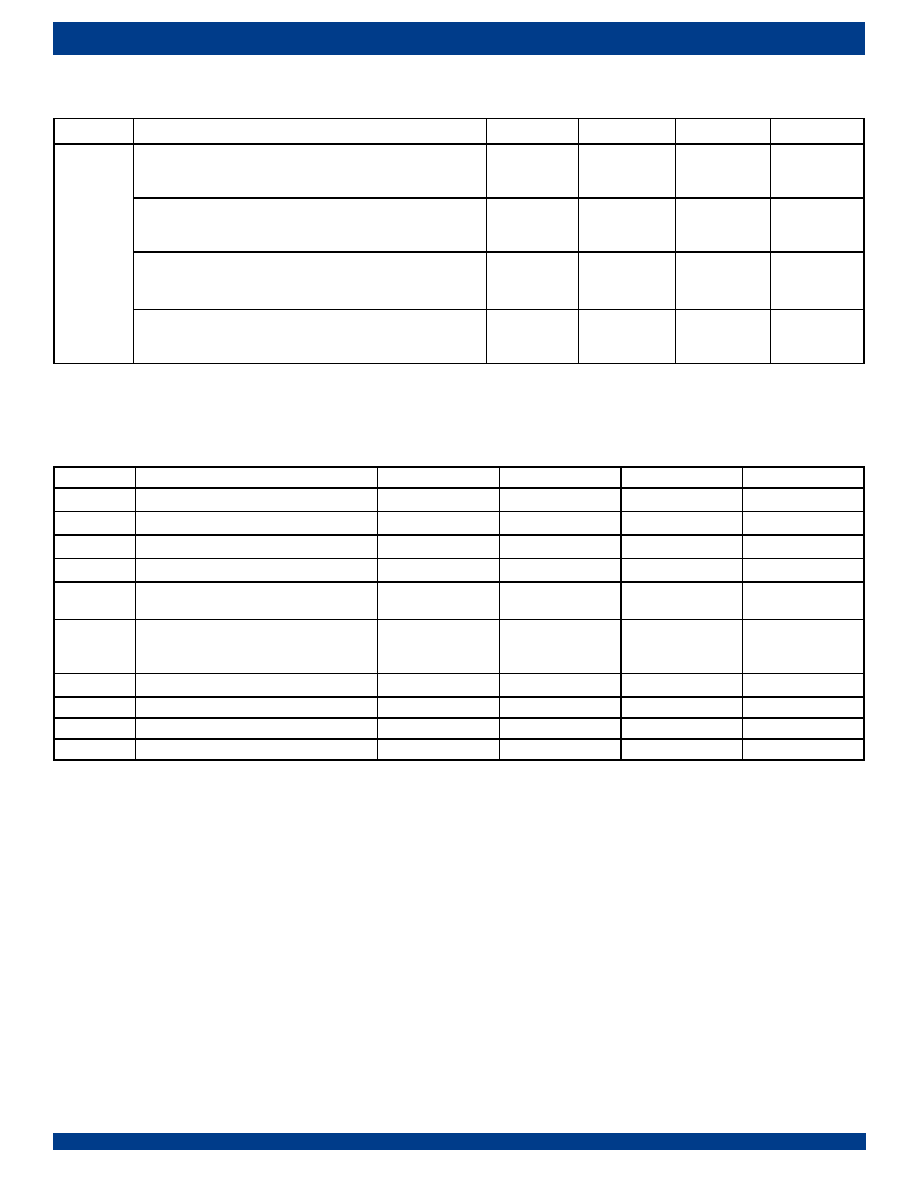
56
INDUSTRIAL
TEMPERATURE RANGES
QUAD CHANNEL T1/E1/J1 LONG HAUL/SHORT HAUL LINE INTERFACE UNIT
1.Maximum power and current consumption over the full operating temperature and power supply voltage range. Includes all channels.
2.Power consumption includes power absorbed by line load and external transmitter components.
3.T1 is measured with maximum cable length.
Table-61 Power Consumption
Symbol Parameter
Min
Typ
Max
1,2
Unit
E1, 3.3 V, 75
Load
50% ones density data:
100% ones density data:
-
-
830
990
-
1110
mW
E1, 3.3 V, 120
Load
50% ones density data:
100% ones density data:
-
-
790
920
-
1050
mW
T1, 3.3 V, 100
Load
3
50% ones density data:
100% ones density data:
-
-
890
1190
-
1320
mW
J1, 3.3 V, 110
Load
50% ones density data:
100% ones density data:
-
-
760
990
1110
mW
Table-62 DC Characteristics
Symbol
Parameter
Min
Typ
Max
Unit
V
IL
Input Low Level Voltage
-
-
0.8
V
V
IH
Input High Voltage
2.0
-
-
V
V
OL
Output Low level Voltage (Iout=1.6mA)
-
-
0.4
V
V
OH
Output High level Voltage (Iout=400
µA)
2.4
-
VDDIO
V
V
MA
Analog Input Quiescent Voltage (RTIP, RRING
pin while floating)
1.5
V
I
I
Input Leakage Current
TMS, TDI, TRST
All other digital input pins
-10
50
10
µA
µA
I
ZL
Tri-state Leakage Current
-10
10
µA
Ci
Input capacitance
15
pF
Co
Output load capacitance
50
pF
Co
Output load capacitance (bus pins)
100
pF

57
INDUSTRIAL
TEMPERATURE RANGES
QUAD CHANNEL T1/E1/J1 LONG HAUL/SHORT HAUL LINE INTERFACE UNIT
Table-63 E1 Receiver Electrical Characteristics
Symbol
Parameter
Min
Typ
Max
Unit
Test conditions
Receiver sensitivity
Short haul with cable loss@1024kHz:
Long haul with cable loss@1024kHz:
-10
-43
dB
Analog LOS level
Short haul
Long haul
-4
800
-48
mVp-p
dB
A LOS level is programmable for Long Haul
Allowable consecutive zeros before LOS
G.775:
I.431/ETSI300233:
32
2048
LOS reset
12.5
% ones
G.775, ETSI 300 233
Receive Intrinsic Jitter
20Hz - 100kHz
0.05
U.I.
JA enabled
Input Jitter Tolerance
1 Hz ≠ 20 Hz
20 Hz ≠ 2.4 KHz
18 KHz ≠ 100 KHz
37
5
2
U.I.
U.I.
U.I.
G.823, with 6 dB cable attenuation
ZDM
Receiver Differential Input Impedance
20
K
Internal mode
Input termination resistor tolerance
±1%
RRX
Receive Return Loss
51 KHz ≠ 102 KHz
102 KHz - 2.048 MHz
2.048 MHz ≠ 3.072 MHz
20
20
20
dB
dB
dB
G.703 Internal termination
RPD
Receive path delay
Single rail
Dual rail
7
2
U.I.
U.I.
JA disabled

58
INDUSTRIAL
TEMPERATURE RANGES
QUAD CHANNEL T1/E1/J1 LONG HAUL/SHORT HAUL LINE INTERFACE UNIT
Table-64 T1/J1 Receiver Electrical Characteristics
Symbol
Parameter
Min
Typ
Max
Unit
Test conditions
receiver sensitivity
Short haul with cable loss@772kHz:
Long haul with cable loss@772kHz:
-10
-36
dB
Analog LOS level
Short haul
Long haul
-4
800
-48
mVp-p
dB
A LOS level is programmable for Long Haul
Allowable consecutive zeros before LOS
T1.231-1993
I.431
175
1544
LOS reset
12.5
% ones G.775, ETSI 300 233
Receive Intrinsic Jitter
10 Hz ≠ 8 KHz
10 Hz ≠ 40 KHz
8 KHz ≠ 40 KHz
Wide band
0.02
0.025
0.025
0.050
U.I.
U.I.
U.I.
U.I.
JA enabled ( in receive path)
Input Jitter Tolerance
0.1 Hz ≠ 1 Hz
4.9 Hz ≠ 300 Hz
10 KHz ≠ 100 KHz
138.0
28.0
0.4
U.I.
U.I.
U.I.
AT&T62411
ZDM
Receiver Differential Input Impedance
20
K
Internal mode
Input termination resistor tolerance
±1%
RRX
Receive Return Loss
39 KHz ≠ 77 KHz
77 KHz - 1.544 MHz
1.544 MHz ≠ 2.316 MHz
20
20
20
dB
dB
dB
G.703
Internal termination
RPD
Receive path delay
Single rail
Dual rail
7
2
U.I.
U.I.
JA disabled

59
INDUSTRIAL
TEMPERATURE RANGES
QUAD CHANNEL T1/E1/J1 LONG HAUL/SHORT HAUL LINE INTERFACE UNIT
Table-65 E1 Transmitter Electrical Characteristics
Symbol
Parameter
Min
Typ
Max
Unit
Vo-p
Output pulse amplitudes
E1, 75
load
E1, 120
load
2.14
2.7
2.37
3.0
2.60
3.3
V
V
Vo-s
Zero (space) level
E1, 75
load
E1, 120
load
-0.237
-0.3
0.237
0.3
V
V
Transmit amplitude variation with supply
-1
+1
%
Difference between pulse sequences for 17 consecutive pulses (T1.102)
200
mV
Tpw
Output Pulse Width at 50% of nominal amplitude
232
244
256
ns
Ratio of the amplitudes of Positive and Negative Pulses at the center of the pulse interval
(G.703)
0.95
1.05
Ratio of the width of Positive and Negative Pulses at the center of the pulse interval (G.703)
0.95
1.05
RTX
Transmit Return Loss (G.703)
51 KHz ≠ 102 KHz
102 KHz - 2.048 MHz
2.048 MHz ≠ 3.072 MHz
20
15
12
dB
dB
dB
JTXp-p
Intrinsic Transmit Jitter (TCLK is jitter free)
20 Hz ≠ 100 KHz
0.050
U.I.
Td
Transmit path delay (JA is disabled)
Single rail
Dual rail
8.5
4.5
U.I.
U.I.
Isc
Line short circuit current
180
mA
Ip-p

60
INDUSTRIAL
TEMPERATURE RANGES
QUAD CHANNEL T1/E1/J1 LONG HAUL/SHORT HAUL LINE INTERFACE UNIT
Table-66 T1/J1 Transmitter Electrical Characteristics
Symbol
Parameter
Min
Typ
Max
Unit
Vo-p
Output pulse amplitudes
2.4
3.0
3.6
V
Vo-s
Zero (space) level
-0.15
0.15
V
Transmit amplitude variation with supply
-1
+1
%
Difference between pulse sequences for 17 consecutive
pulses(T1.102)
200
mV
TPW
Output Pulse Width at 50% of nominal amplitude
338
350
362
ns
Pulse width variation at the half amplitude (T1.102)
20
ns
Imbalance between Positive and Negative Pulses amplitude
(T1.102)
0.95
1.05
Output power level (T1.102)
@772kHz
@1544kHz (referenced to power at 772kHz)
12.6
-29
17.9
dBm
dBm
RTX
Transmit Return Loss
39 KHz ≠ 77 KHz
77 KHz ≠ 1.544 MHz
1.544 MHz ≠ 2.316 MHz
20
15
12
dB
dB
dB
JTXP-P
Intrinsic Transmit Jitter (TCLK is jitter free)
10 Hz ≠ 8 KHz
8 KHz ≠ 40 KHz
10 Hz ≠ 40 KHz
wide band
0.020
0.025
0.025
0.050
U.I.p-p
U.I.p-p
U.I.p-p
U.I.p-p
Td
Transmit path delay (JA is disabled)
Single rail
Dual rail
8.5
4.5
U.I.
U.I.
I
SC
Line short circuit current
180
mA
Ip-p

61
INDUSTRIAL
TEMPERATURE RANGES
QUAD CHANNEL T1/E1/J1 LONG HAUL/SHORT HAUL LINE INTERFACE UNIT
1.Relative to nominal frequency, MCLK= ± 100 ppm
2.RCLK duty cycle widths will vary depending on extent of received pulse jitter displacement. Maximum and minimum RCLK duty cycles are for worst case jitter conditions
(0.2UI displacement for E1 per ITU G.823).
3.For all digital outputs. C load = 15pF
Table-67 Transmitter and Receiver Timing Characteristics
Symbol
Parameter
Min
Typ
Max
Unit
MCLK frequency
E1:
T1/J1:
2.048/49.152
1.544/37.056
MHz
MCLK tolerance
-100
100
ppm
MCLK duty cycle
30
70
%
Transmit path
TCLK frequency
E1:
T1/J1:
2.048
1.544
MHz
TCLK tolerance
-50
+50
ppm
TCLK Duty Cycle
10
90
%
t1
Transmit Data Setup Time
40
ns
t2
Transmit Data Hold Time
40
ns
Delay time of THZ low to driver high impedance
10
us
Delay time of TCLK low to driver high impedance
75
U.I.
Receive path
Clock recovery capture
range
1
E1
± 80
ppm
T1/J1
± 180
RCLK duty cycle
2
40
50
60
%
t4
RCLK pulse width
2
E1:
T1/J1:
457
607
488
648
519
689
ns
t5
RCLK pulse width low time
E1:
T1/J1:
203
259
244
324
285
389
ns
t6
RCLK pulse width high time
E1:
T1/J1:
203
259
244
324
285
389
ns
Rise/fall time
3
20
ns
t7
Receive Data Setup Time
E1:
T1/J1:
200
200
244
324
ns
t8
Receive Data Hold Time
E1:
T1/J1:
200
200
244
324
ns

62
INDUSTRIAL
TEMPERATURE RANGES
QUAD CHANNEL T1/E1/J1 LONG HAUL/SHORT HAUL LINE INTERFACE UNIT
Figure-23 Transmit System Interface Timing
Figure-24 Receive System Interface Timing
Table-68 Jitter Tolerance
Jitter Tolerance
Min
Typ
Max
Unit
Standard
E1: 1 Hz
20 Hz ≠ 2.4 KHz
18 KHz ≠ 100 KHz
37
1.5
0.2
U.I.
U.I.
U.I.
G.823
Cable attenuation is 6dB
T1/J1: 1 Hz
4.9 Hz ≠ 300 Hz
10 KHz ≠ 100 KHz
138.0
28.0
0.4
U.I.
U.I.
U.I.
AT&T 62411
TDNn
TDn/TDPn
TCLKn
t1
t2
RDNn/CVn
RDPn/RDn
RCLKn
t4
t7
t6
t7
t5
t8
t8
(RCLK_SEL = 1)
(RCLK_SEL = 0)
RDPn/RDn
RDNn/CVn
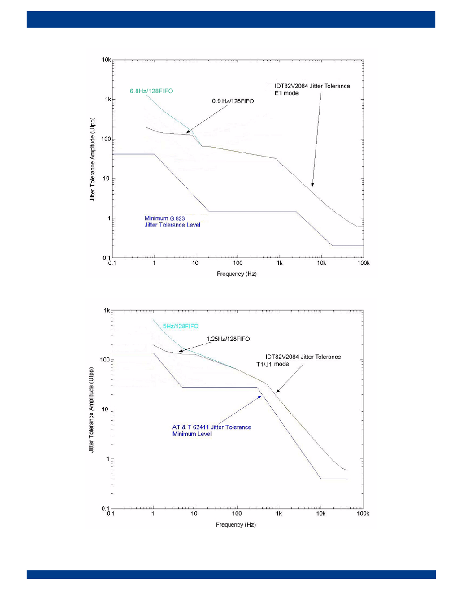
63
INDUSTRIAL
TEMPERATURE RANGES
QUAD CHANNEL T1/E1/J1 LONG HAUL/SHORT HAUL LINE INTERFACE UNIT
Figure-25 E1 Jitter Tolerance Performance
Figure-26 T1/J1 Jitter Tolerance Performance

64
INDUSTRIAL
TEMPERATURE RANGES
QUAD CHANNEL T1/E1/J1 LONG HAUL/SHORT HAUL LINE INTERFACE UNIT
Table-69 Jitter Attenuator Characteristics
Parameter
Min Typ
Max
Unit
Jitter Transfer Function Corner (-3dB) Frequency
E1, 32/64/128 bits FIFO
JABW = 0:
JABW = 1:
T1/J1, 32/64/128 bits FIFO
JABW = 0:
JABW = 1:
6.8
0.9
5
1.25
Hz
Hz
Hz
Hz
Jitter Attenuator
E1: (G.736)
@ 3 Hz
@ 40 Hz
@ 400 Hz
@ 100 kHz
T1/J1: (Per AT&T pub.62411)
@ 1 Hz
@ 20 Hz
@ 1 kHz
@ 1.4 kHz
@ 70 kHz
-0.5
-0.5
+19.5
+19.5
dB
0
0
+33.3
40
40
Jitter Attenuator Latency Delay
32 bits FIFO:
64 bits FIFO:
128 bits FIFO:
16
32
64
U.I.
U.I.
U.I.
Input jitter tolerance before FIFO overflow or underflow
32 bits FIFO:
64 bits FIFO:
128 bits FIFO:
28
58
120
U.I.
U.I.
U.I.

65
INDUSTRIAL
TEMPERATURE RANGES
QUAD CHANNEL T1/E1/J1 LONG HAUL/SHORT HAUL LINE INTERFACE UNIT
Figure-27 E1 Jitter Transfer Performance
Figure-28 T1/J1 Jitter Transfer Performance
66
INDUSTRIAL
TEMPERATURE RANGES
QUAD CHANNEL T1/E1/J1 LONG HAUL/SHORT HAUL LINE INTERFACE UNIT
Figure-29 JTAG Interface Timing
Table-70 JTAG Timing Characteristics
Symbol Parameter
Min
Typ
Max
Unit
t1
TCK Period
100
ns
t2
TMS to TCK Setup Time
TDI to TCK Setup Time
25
ns
t3
TCK to TMS Hold Time
TCK to TDI Hold Time
25
ns
t4
TCK to TDO Delay Time
50
ns
TCK
t1
t2
t3
TDO
TMS
TDI
t4
67
INDUSTRIAL
TEMPERATURE RANGES
QUAD CHANNEL T1/E1/J1 LONG HAUL/SHORT HAUL LINE INTERFACE UNIT
7
MICROCONTROLLER INTERFACE TIMING CHARACTERISTICS
7.1
SERIAL INTERFACE TIMING
Figure-30 Serial Interface Write Timing
Figure-31 Serial Interface Read Timing with SCLKE=1
Figure-32 Serial Interface Read Timing with SCLKE=0
Table-71 Serial Interface Timing Characteristics
Symbol
Parameter
Min
Typ
Max
Unit
Comments
t1
SCLK High Time
82
ns
t2
SCLK Low Time
82
ns
t3
Active CS to SCLK Setup Time
5
ns
t4
Last SCLK Hold Time to Inactive CS Time
41
ns
t5
CS Idle Time
41
ns
t6
SDI to SCLK Setup Time
0
ns
t7
SCLK to SDI Hold Time
62
ns
t10
SCLK to SDO Valid Delay Time
75
ns
t11
Inactive CS to SDO tri-state Hold Time
70
ns
MSB
LSB
LSB
CS
SCLK
SDI
t1
t2
t3
t4
t5
t6
t7
t7
1
2
3
4
5
15
16
17
18
19
20
21
22
23
24
SDO
CS
SCLK
t4
t11
t10
7
6
5
4
3
2
1
0
1
2
3
4
5
15
16
17
18
19
20
21
22
23
24
SDO
CS
SCLK
t4
t11
t10
7
6
5
4
3
2
1
0

68
INDUSTRIAL
TEMPERATURE RANGES
QUAD CHANNEL T1/E1/J1 LONG HAUL/SHORT HAUL LINE INTERFACE UNIT
7.2
PARALLEL INTERFACE TIMING
Figure-33 Non_multiplexed Motorola Read Timing
Table-72 Non_multiplexed Motorola Read Timing Characteristics
Symbol
Parameter
Min
Max
Unit
tRC
Read Cycle Time
190
ns
tDW
Valid DS Width
180
ns
tRWV
Delay from DS to Valid Read Signal
15
ns
tRWH
R/W to DS Hold Time
65
ns
tAV
Delay from DS to Valid Address
15
ns
tADH
Address to DS Hold Time
65
ns
tPRD
DS to Valid Read Data Propagation Delay
175
ns
tDAZ
Delay from DS inactive to data bus High Impedance
5
20
ns
tRecovery
Recovery Time from Read Cycle
5
ns
A[x:0]
Valid Address
DS+CS
R/W
READ D[7:0]
tRWV
Valid Data
tDAZ
tADH
tRWH
tPRD
tRC
tDW
tAV
tRecovery

69
INDUSTRIAL
TEMPERATURE RANGES
QUAD CHANNEL T1/E1/J1 LONG HAUL/SHORT HAUL LINE INTERFACE UNIT
Figure-34 Non_multiplexed Motorola Write Timing
Table-73 Non_multiplexed Motorola Write Timing Characteristics
Symbol
Parameter
Min
Max
Unit
tWC
Write Cycle Time
120
ns
tDW
Valid DS Width
100
ns
tRWV
Delay from DS to Valid Write Signal
15
ns
tRWH
R/W to DS Hold Time
65
ns
tAV
Delay from DS to Valid Address
15
ns
tAH
Address to DS Hold Time
65
ns
tDV
Delay from DS to Valid Write Data
15
ns
tDHW
Write Data to DS Hold Time
65
ns
tRecovery
Recovery Time from Write Cycle
5
ns
A[x:0]
Valid Address
DS+CS
R/W
Write D[7:0]
tRWV
tDHW
tAH
tRWH
tWC
tDW
tAV
Valid Data
tDV
tRecovery

70
INDUSTRIAL
TEMPERATURE RANGES
QUAD CHANNEL T1/E1/J1 LONG HAUL/SHORT HAUL LINE INTERFACE UNIT
Figure-35 Non_multiplexed Intel Read Timing
Table-74 Non_multiplexed Intel Read Timing Characteristics
Symbol
Parameter
Min
Max
Unit
tRC
Read Cycle Time
190
ns
tRDW
Valid RD Width
180
ns
tAV
Delay from RD to Valid Address
15
ns
tAH
Address to RD Hold Time
65
ns
tPRD
RD to Valid Read Data Propagation Delay
175
ns
tDAZ
Delay from RD inactive to data bus High Impedance
5
20
ns
tRecovery
Recovery Time from Read Cycle
5
ns
A[x:0]
Valid Address
CS+RD
READ D[7:0]
Valid Data
tDAZ
tAH
tPRD
tRDW
tAV
Note: WR should be tied to high
tRecovery
tRC

71
INDUSTRIAL
TEMPERATURE RANGES
QUAD CHANNEL T1/E1/J1 LONG HAUL/SHORT HAUL LINE INTERFACE UNIT
Figure-36 Non_multiplexed Intel Write Timing
Table-75 Non_multiplexed Intel Write Timing Characteristics
Symbol
Parameter
Min
Max
Unit
tWC
Write Cycle Time
120
ns
tWRW
Valid WR Width
100
ns
tAV
Delay from WR to Valid Address
15
ns
tAH
Address to WR Hold Time
65
ns
tDV
Delay from WR to Valid Write Data
15
ns
tDHW
Write Data to WR Hold Time
65
ns
tRecovery
Recovery Time from Write Cycle
5
ns
A[x:0]
Valid Address
WR+CS
Write D[7:0]
tDHW
tAH
tWC
tWRW
tAV
Valid Data
tDV
Note: RD should be tied to high
tRecovery
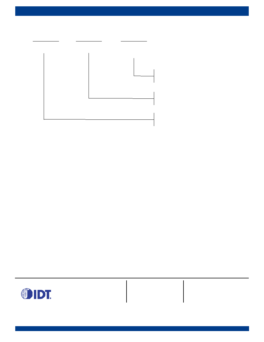
72
INDUSTRIAL
TEMPERATURE RANGES
QUAD CHANNEL T1/E1/J1 LONG HAUL/SHORT HAUL LINE INTERFACE UNIT
CORPORATE HEADQUARTERS
2975 Stender Way
Santa Clara, CA 95054
for SALES:
800-345-7015 or 408-727-6116
fax: 408-492-8674
www.idt.com*
for Tech Support:
408-330-1753
email:TELECOMhelp@idt.com
To search for sales office near you, please click the sales button found on our home page or dial the 800# above and press 2.
The IDT logo is a registered trademark of Integrated Device Technology, Inc.
ORDERING INFORMATION
IDT
XXXXXXX
XX
X
Device Type
Blank
Process/
Temperature
Range
PF
82V2084
Industrial (-40 ∞C to +85 ∞C)
Thin Quad Flatpack (TQFP, PK128)
Long Haul/Short Haul LIU