 | –≠–ª–µ–∫—Ç—Ä–æ–Ω–Ω—ã–π –∫–æ–º–ø–æ–Ω–µ–Ω—Ç: AN-136 | –°–∫–∞—á–∞—Ç—å:  PDF PDF  ZIP ZIP |

Integrated Device Technology, Inc.
©
1995 Integrated Device Technology, Inc.
1/95
APPLICATION
NOTE
AN-136
A NEW GENERATION OF
TAG SRAMS--THE IDT71215 AND
IDT71216
By Kelly Maas
CACHE AND TAG BASICS
For those new to caches, a brief review of cache basics may
be worthwhile. A cache is a memory that provides a CPU with
high speed access to a subset of the data from main memory.
Our discussions are focused on the secondary cache, which
is also known as the L2 cache, but it is not much different from
the faster primary (L1) cache residing inside most CPUs.
The cache consists of a controller, a data memory and a tag
memory. The purpose of the data memory is to store the
active data from main memory, and is composed of either
synchronous burst or asynchronous SRAMs. The tag memory
stores indexes (part of the CPU address field) that indicate
which data is stored in the cache. Additionally, most caches
also require at least one bit of memory for each cache entry,
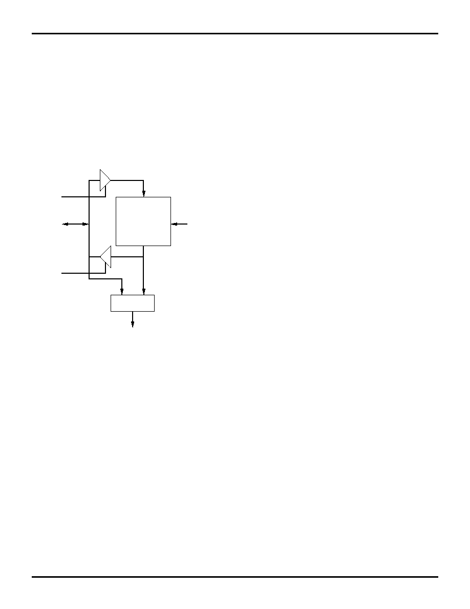
to indicate the valid or dirty status of that entry. Figure 1 shows
how the CPU address field relates to the cache and the tag
memory. This example includes valid and dirty status bits, and
represents a 512KB cache, 2GB cacheable address space,
32-byte line size, and 8-byte word size.
INTRODUCTION
The 71215 and 71216 represent a new generation of
integrated Tag SRAMs. Just as earlier Tag SRAMs such as
the 71B74 were better suited for tag applications than conven-
tional SRAMs, the 71215/16 go a step further by integrating
new features to significantly ease the design of high perfor-
mance cache subsystems for today's high speed processors.
These Tag RAMs are designed for easy interfacing to Intel and
PowerPC processors, but are very flexible and can easily be
used in other applications as well.
This application note first provides some background infor-
mation on caches, then describes in detail the architecture
and operation of the 71215 and 71216. This is followed by
three application examples, then a brief discussion of cache
coherency protocol implementation using these Tag RAMs.
Since the 71215 and 71216 are very similar, the descriptions
and explanations in this application note apply to both unless
otherwise noted.
TAG
ADDRESS
A30
A5
TAG
COMPARATOR
A18
A19
TAG MEMORY
LINE
VALID
A4
A3
12
1
1
LINE
DIRTY
MATCH
DATA SRAM ADDRESS
A31
to CACHE CONTROLLER
MSB
LSB
3176 drw 01
Figure 1. CPU Address Field and the L2 Cache (Showing 512 KB cache size and 2 GB cacheable main memory)
The IDT logo is a registered trademark of Integrated Device Technology, Inc.
PowerPC is a trademark of International Business Machines Corporation
Pentium is a trademark of Intel Corporation
2
A NEW GENERATION OF TAG SRAMS--THE IDT71215 AND IDT71216
APPLICATION NOTE AN-136
Integrated Tag RAMs operate as ordinary SRAMs, but
have an additional access mode in which a word of data (an
index) is internally read (but not driven off-chip) and compared
with the CPU address driven onto the Tag RAM's data bus.
Figure 2 shows the basic architecture of an integrated Tag
SRAM. The comparator indicates whether the cache holds
the data for the address supplied by the CPU or other bus
master. This is a critical timing path since this tag "hit" or "miss"
must be determined before the cache memory access can be
completed (or even started, in many cases). Note that tag
memories connect only to the CPU address bus and never to
the CPU data bus.
BASIC TAG RAM ARCHITECTURE
DATA
IN
DATA
OUT
MEMORY
ADDRESS
DATA
(TAG)
WRITE
READ
COMPARE
MATCH
3176 drw 02
Figure 2. Basic Integrated Tag SRAM Architecture
An additional feature of the Tag SRAM is that a portion of
the memory is resettable. This permits use of one bit of the
data field as a "valid" status bit. Upon system initialization,
when the cache contains random data, a quick reset will clear
the valid bit for every cache line so that all initial cache
accesses will result in a miss. A miss then causes the address
to be loaded into the Tag RAM, data from main memory to be
loaded into the data RAMs, and the valid bit to be set true. If
not included in the Tag RAM, this function requires an addi-
tional 1-bit wide SRAM.
The reset feature of earlier Tag RAMs was sufficient for
implementation of a valid bit, but nothing more. Today's
secondary caches frequently implement four-state write-back
protocols such as MESI, with multiprocessor applications
requiring five states (e.g. MOESI) or more. Hence, most
caches need a two- or three-bit status memory that is ac-
cessed separately from the tag memory. It is used in conjunc-
tion with the match output to determine the response to a CPU
memory access or a snoop. (A snoop is an operation initiated
by the system in order to maintain coherency between the
cache(s) and main memory.) This has typically been handled
with yet another RAM - a conventional separate I/O SRAM
organized as either x1 or x4. The 71215/16 includes a three-
bit status memory on chip.
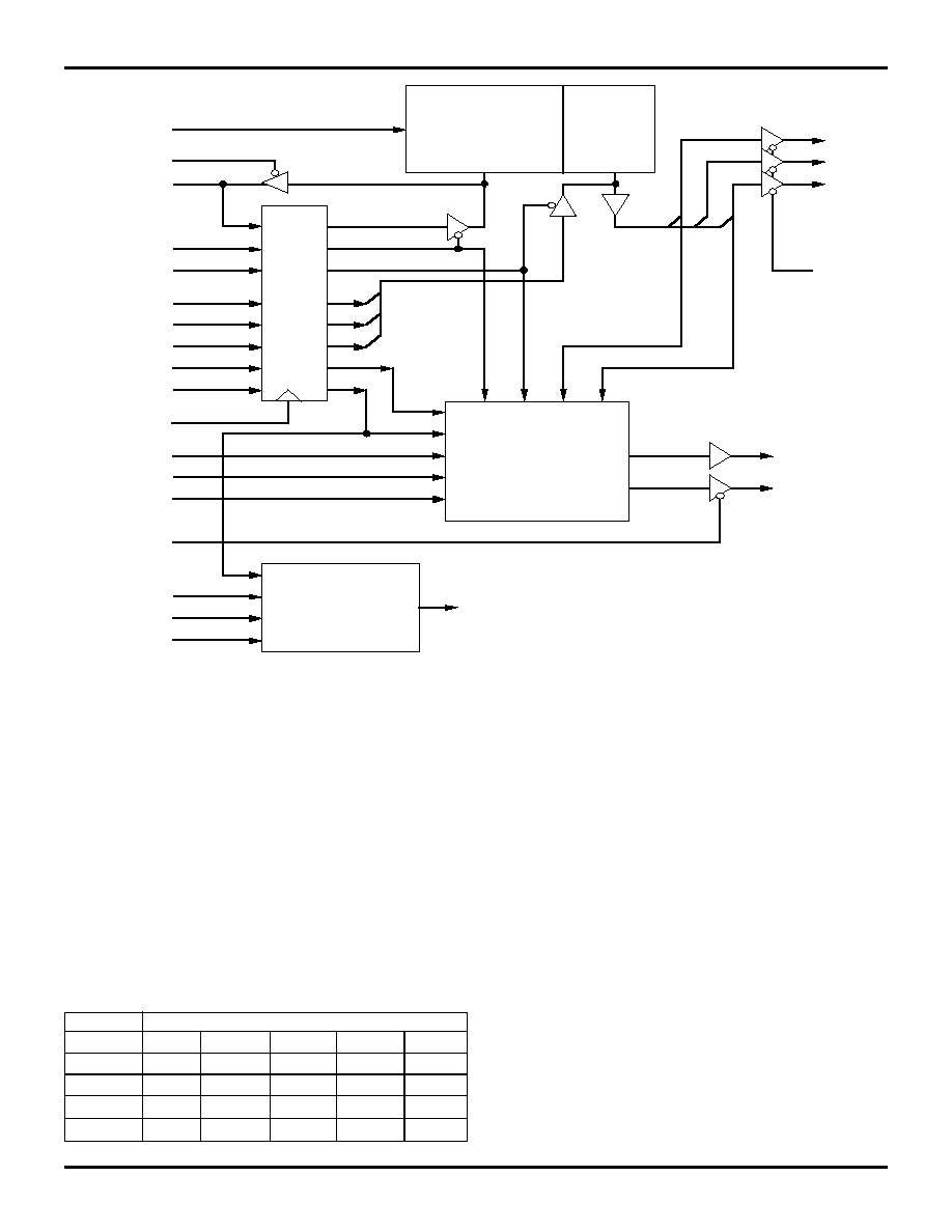
THE 71215 AND 71216
As shown in Figure 3, these 16K x 15 RAMs are configured
internally as two memories: 16K x 12 for tag and 16K x 3 for
status. These two memories share the address bus but are
controlled independently. An important new feature is extra
pins and logic for generating
BRDY
(Intel's Burst Ready) and
TA
(PowerPC's Transfer Acknowledge). These are CPU input
signals which are time critical in zero wait state secondary
caches. I/O's are 3.3V compatible and there is a low power
standby mode. All writes are synchronous as with burst data
SRAMs, while all reads and compares are asynchronous for
minimum delay. Two opposite polarity chip select pins are
provided for easy depth expansion.
3
A NEW GENERATION OF TAG SRAMS--THE IDT71215 AND IDT71216
APPLICATION NOTE AN-136
Figure 3. Simplified 71215 / 71216 Block Diagram (71216 signal names are in parenthesis)
For a 1MB cache and 4GB of cacheable main memory, two
of the devices may be cascaded in depth without any timing
penalty apart from increased capacitive loading. This is
accomplished with the two Chip Select pins. A low order
address signal may be connected to
CS1
on one chip and to
CS2 on the other so that at any given time, one is selected and
the other is deselected. The deselected chip ignores all
control inputs (except
RESET
and
PWRDN
) and tri-states its
outputs so that the two chips can be conveniently bussed
together. As expected, worst case timing delays from the Chip
Select inputs are the same as for the Address inputs. When
only a single 71215 or 71216 is used in an application,
CS1
is
tied to V
SS
and CS2 is tied to V
CC
.
With a 16K x 12 tag memory, the 71215 and 71216 are
wider and deeper than most Tag RAMs. For a typical 64-bit
CPU with a 32-byte line size, the 16K depth supports a 512KB
cache while the 12-bit tag field supports 2GB of cacheable
main memory. Thus, only a single component is required for
most applications. Table 1 shows the relationships between
Tag RAM size, cache size, and cacheable main memory size.
The Tag depth is equal to the cache size divided by the line
size. The Tag width is equal to the base-2 log of the ratio of
main memory size to cache size.
TABLE 1: REQUIRED TAG RAM SIZE AS A
FUNCTION OF CACHE SIZE AND MAIN
MEMORY SIZE
(For 32-byte line size and direct
mapped cache architecture.)
Cache Size
Cacheable Main Memory Size
64MB
256MB
1GB
2GB
4GB
128KB
4K x 9
4K x 11
4K x 13
4K x 14
4K x 15
256KB
8K x 8
8K x 10
8K x 12
8K x 13
8K x 14
512KB
16K x 7
16K x 9
16K x 11 16K x 12 16K x 13
1MB
32K x 6
32K x 8
32K x 10 32K x 11 32K x 12
3176 tbl 01
CLK
CS2
BRDYH (TAH)
MATCH
SFUNC
ADDR(0:13)
VLDin / S1
IN
DLYin / S2
IN
WTin / S3
IN
VLD
OUT
DLY
OUT
WT
OUT
CS1
BRDYIN
(TAIN)
PWRDN
BRDYOE (TAOE)
W/
R
(TT1)
WET
WES
BRDY
(
TA
)
REGISTER
16K x 12
MEMORY
TAG (0:11)
OET
16K x 3
MEMORY
MATCH AND
BRDY LOGIC
Chip enabling
Reseting the 16K x 3 memory
Powering down
Disabling outputs
CONTROL
LOGIC
OES
RESET
3176 drw 03
4
A NEW GENERATION OF TAG SRAMS--THE IDT71215 AND IDT71216
APPLICATION NOTE AN-136
Figure 4. Detailed 71215 / 71216 Block Diagram (71216 pin names are in parenthesis)
CLK
SFUNC
ADDR (13:0)
VLD/S1
OUT
DLY/S2
OUT
WT/S3
OUT
RESET
WET
WES
REGISTER
16K x 12
MEMORY
TAG
TAG (11:0)
OET
16K x 3
MEMORY
STATUS
MATCH
BRDYH (TAH)
BRDYOE
(
TAOE
)
W/
R
(TT1)
BRDY
(
TA
)
BRDYIN
(
TAIN
)
VLD/S1
IN
DLY/S2
IN
WT/S3
IN
SA
CS2
CS1
RESET
(neg) PULSE
GENERATOR
PWRDN
Data
IN
Register
Data
IN
Register
WRITE
(pos) PULSE
GENERATOR
Register
SA
COMPARE
Reg
0
1
OES
REG-
ISTER
71216 only
3176 drw 04
5
A NEW GENERATION OF TAG SRAMS--THE IDT71215 AND IDT71216
APPLICATION NOTE AN-136
The 71215/16 is shown in more detail in Figure 4. The tag
memory is controlled by the Write Enable Tag (
WET
) and
Output Enable Tag (
OET
) pins. During writes,
WET
is synchro-
nous to CLK, as are the input data (TAG0 - TAG11) and
address (A0 - A13). Note that
WET
has no effect on the TAG
output buffers, so
OET
must be high to disable the outputs
during writes. Reads are performed by deasserting
WET
and
asynchronously asserting
OET
. For cache architectures in
which the tag is never read (e.g. write-through caches),
OET
may be tied to V
CC
. When both
WET
and
OET
are high, the
71215/16 is in the match mode, where the TAG0 - TAG11
inputs are compared with the stored data and are used to
generate the MATCH and
BRDY
/
TA
outputs. In both read and
match modes, the address path is flow-through for the fastest
possible response to a new address.
The three status bits of the 71215/16 are labeled VLD/S1,
DTY/S2, and WT/S3. The reason for the dual names is that
their functions vary, dependent on the state of the static Status
Function (SFUNC) input signal. When SFUNC is low, the
status bits are said to be in a "dedicated" mode and are
referred to as Valid, Dirty and Write-Through. See Figure 5.
When SFUNC is high, the status bits play no special role within
the 71215/16 and are simply referred to as Status 1, Status 2
and Status 3. See Figure 6. The functionality of VLD and WT
in the dedicated mode is described later. DTY/S2 does not
have any special functionality within the 71215/16.
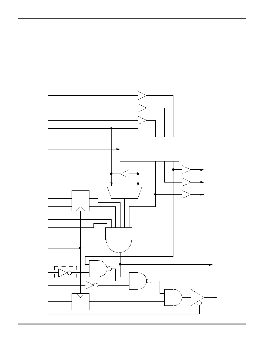
Figure 5. Dedicated Mode Logic (71216 pin names are in parenthesis)
I/O
Address
V
D
WP
MATCH
W/
R
(TT1)
BRDYH (TAH)
BRDYOE
(
TAOE
)
COMPARE
MEMORY
WT
IN
/ S3
IN
DTY
IN
/ S2
IN
VLD
IN
/ S1
IN
WT
OUT
/ S3
OUT
DTY
OUT
/ S2
OUT
VLD
OUT
/ S1
OUT
BRDY
(
TA
)
BRDY
IN
(
TAIN
)
CLK
WES
WET
internal RESET
OE
71216 only
3176 drw 05