 | –≠–ª–µ–∫—Ç—Ä–æ–Ω–Ω—ã–π –∫–æ–º–ø–æ–Ω–µ–Ω—Ç: CSPT857 | –°–∫–∞—á–∞—Ç—å:  PDF PDF  ZIP ZIP |
1
IDTCSPT857/A
2.5V PLL DIFFERENTIAL 1:10 SDRAM CLOCK DRIVER
COMMERCIAL AND INDUSTRIAL TEMPERATURE RANGES
2002 Integrated Device Technology, Inc.
DSC-5172/7
c
IDTCSPT857/A
PRELIMINARY
COMMERCIAL AND INDUSTRIAL TEMPERATURE RANGES
2.5V PHASE LOCKED LOOP
DIFFERENTIAL 1:10 SDRAM
CLOCK DRIVER
Y0
Y0
FBOUT
Y1
Y1
Y5
Y5
Y4
Y4
Y3
Y3
Y2
Y2
Y8
Y8
Y6
Y6
Y7
Y7
Y9
Y9
FBOUT
3/A1
2/A2
5/B2
6/B1
10/D1
9/D2
20/J2
19/J1
22/K1
23/K2
46/A6
47/A5
44/B5
43/B6
39/D6
40/D5
29/J5
30/J6
27/K6
26/K5
32/H6
33/H5
PLL
CLK
PWRDWN
37/E6
CLK
13/F1
14/F2
36/F6
35/F5
16/G2
FBIN
FBIN
TEST
MODE
LOGIC
AV
DD
OCTOBER 2002
The IDT logo is a registered trademark of Integrated Device Technology, Inc.
FEATURES:
∑ Optimized for clock distribution in DDR (Double Data Rate)
SDRAM applications
∑ Operating frequency: 60MHz to 200MHz
∑ Standard speed: PC1600 (DDR200), PC2100 (DDR266)
∑ A speed: PC1600 (DDR200), PC2100 (DDR266), PC2700 (DDR333)
∑ 1 to 10 differential clock distribution
∑ Very low skew (<100ps)
∑ Very low jitter (<75ps)
∑ 2.5V AV
DD
and 2.5V V
DDQ
∑ CMOS control signal input
∑ Test mode enables buffers while disabling PLL
∑ Low current power-down mode
∑ Tolerant of Spread Spectrum input clock
∑ Available in 48-pin TSSOP and 56-pin VFBGA packages
DESCRIPTION:
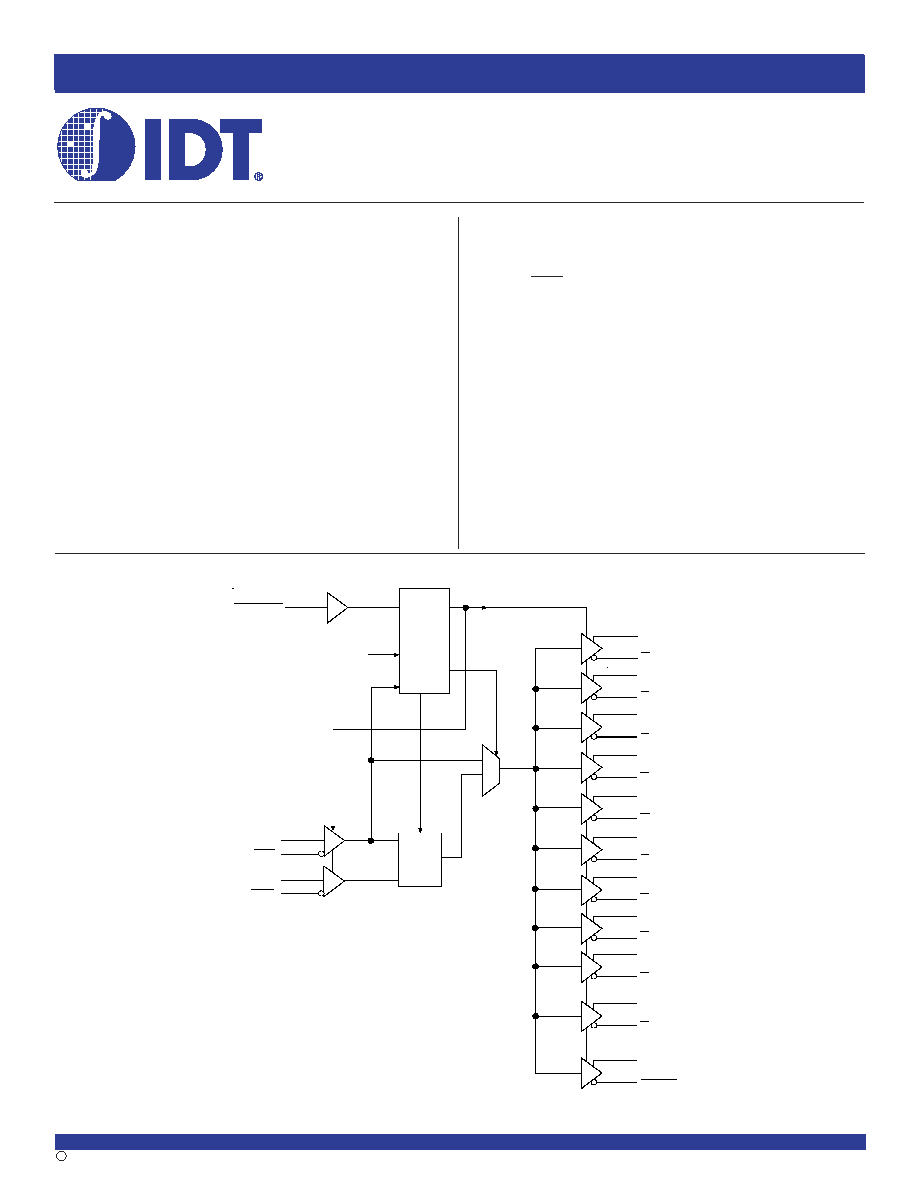
The CSPT857 is a PLL based clock driver that acts as a zero delay buffer
to distribute one differential clock input pair(CLK, CLK ) to 10 differential output
pairs (Y
[0:9]
, Y
[0:9]
) and one differential pair of feedback clock output (FBOUT,
FBOUT). External feedback pins (FBIN, FBIN) for synchronization of the
outputs to the input reference is provided. A CMOS Enable/Disable pin is
available for low power disable. When the output frequency falls below
approximately 20MHz, the device will enter power down mode. In this mode,
the receivers are disabled, the PLL is turned off, and the output clock drivers
are tristated, resulting in a current consumption device of less than 200
µA.
The CSPT857 requires no external components and has been optimised
for very low I/O phase error, skew, and jitter, while maintaining frequency and
duty cycle over the operating voltage and temperature range. The CSPT857,
designed for use in both module assemblies and system motherboard based
solutions, provides an optimum high-performance clock source.
The CSPT857 is only available in Industrial Temperature Range (-40
∞
C to
+85
∞
C), and CSPT857A is only available in Commercial Temperature Range
(0
∞
C to +70
∞
C). See Ordering Information for details.
FUNCTIONAL BLOCK DIAGRAM
2
COMMERCIAL AND INDUSTRIAL TEMPERATURE RANGES
IDTCSPT857/A
2.5V PLL DIFFERENTIAL 1:10 SDRAM CLOCK DRIVER
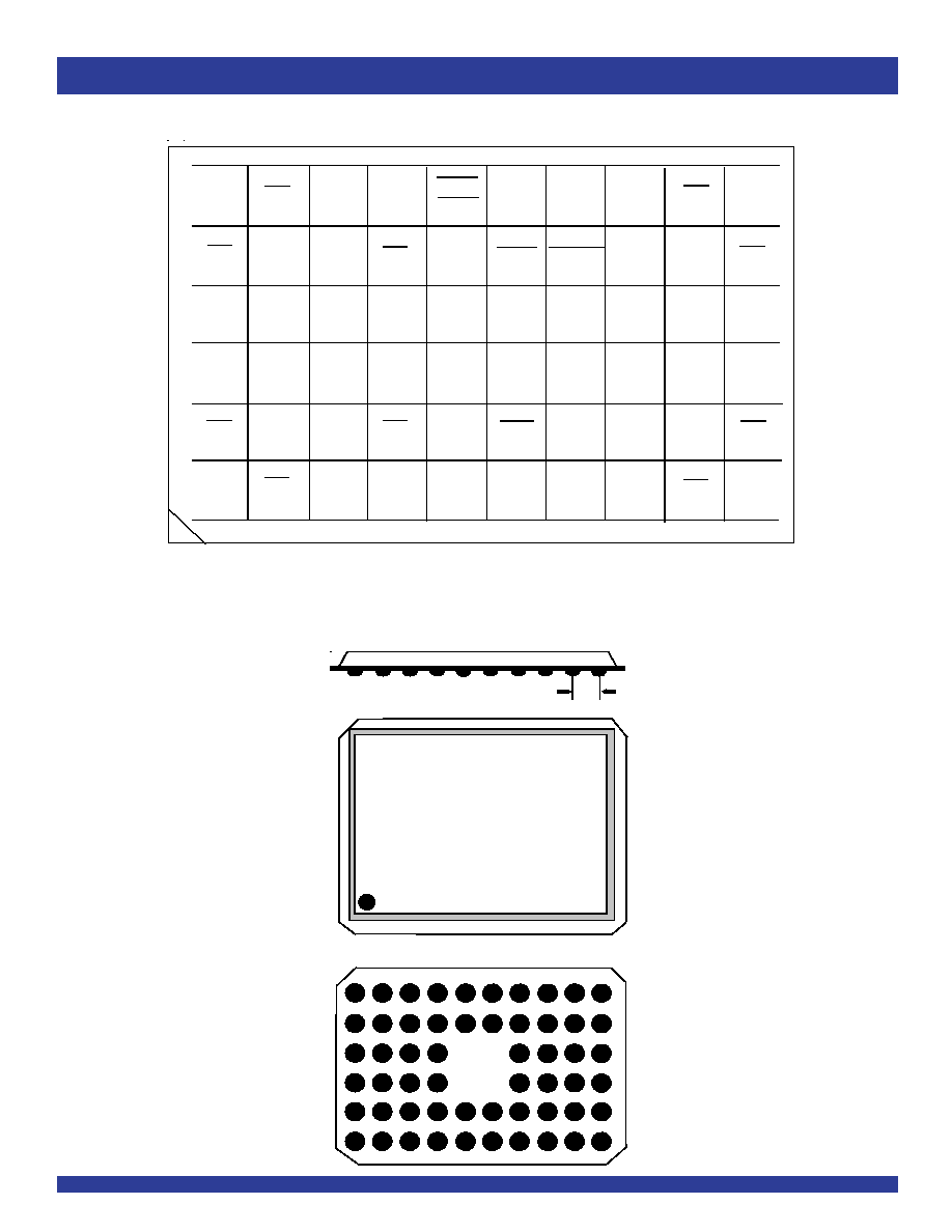
PIN CONFIGURATIONS
56 BALL VFBGA PACKAGE LAYOUT
A
B
C
E
F
G
H
J
K
D
6
5
4
3
2
1
Y
7
V
DDQ
PWR
DWN
FBIN
FBOUT
Y
6
GND
Y
7
V
DDQ
GND
FBIN FBOUT
Y
5
Y
6
Y
5
GND
Y
8
Y
9
Y
9
Y
8
Y
0
Y
0
Y
1
Y
1
Y
2
Y
4
Y
3
Y
2
V
DDQ
GND
GND
GND
V
DDQ
V
DDQ
GND
V
DDQ
GND
GND
V
DDQ
V
DDQ
CLK
CLK
AV
DD
V
DDQ
GND
AGND
Y
4
Y
3
NC
NC
NC
NC
NC
NC
NC
NC
VFBGA
TOP VIEW
0.65mm
TOP VIEW
A B C D E F G H J K
A B C D E F G H J K
1
2
3
4
5
6
1
3
2
4
5
6
3
IDTCSPT857/A
2.5V PLL DIFFERENTIAL 1:10 SDRAM CLOCK DRIVER
COMMERCIAL AND INDUSTRIAL TEMPERATURE RANGES
V
DDQ
GND
2
3
4
5
6
7
8
9
10
11
12
13
14
15
16
17
18
19
20
21
22
23
24
47
46
45
44
43
42
41
40
39
38
37
36
35
34
33
48
32
31
30
29
1
V
DDQ
V
DDQ
GND
25
26
27
28
GND
Y
5
Y
5
GND
Y
0
Y
0
Y
1
Y
1
GND
Y
2
Y
2
CLK
CLK
AV
DD
Y
3
Y
3
V
DDQ
Y
4
Y
6
Y
6
GND
Y
7
Y
7
PWRDWN
FBIN
FBIN
V
DDQ
FBOUT
FBOUT
Y
8
Y
8
V
DDQ
Y
9
Y
9
GND
GND
GND
Y
4
GND
V
DDQ
V
DDQ
V
DDQ
AGND
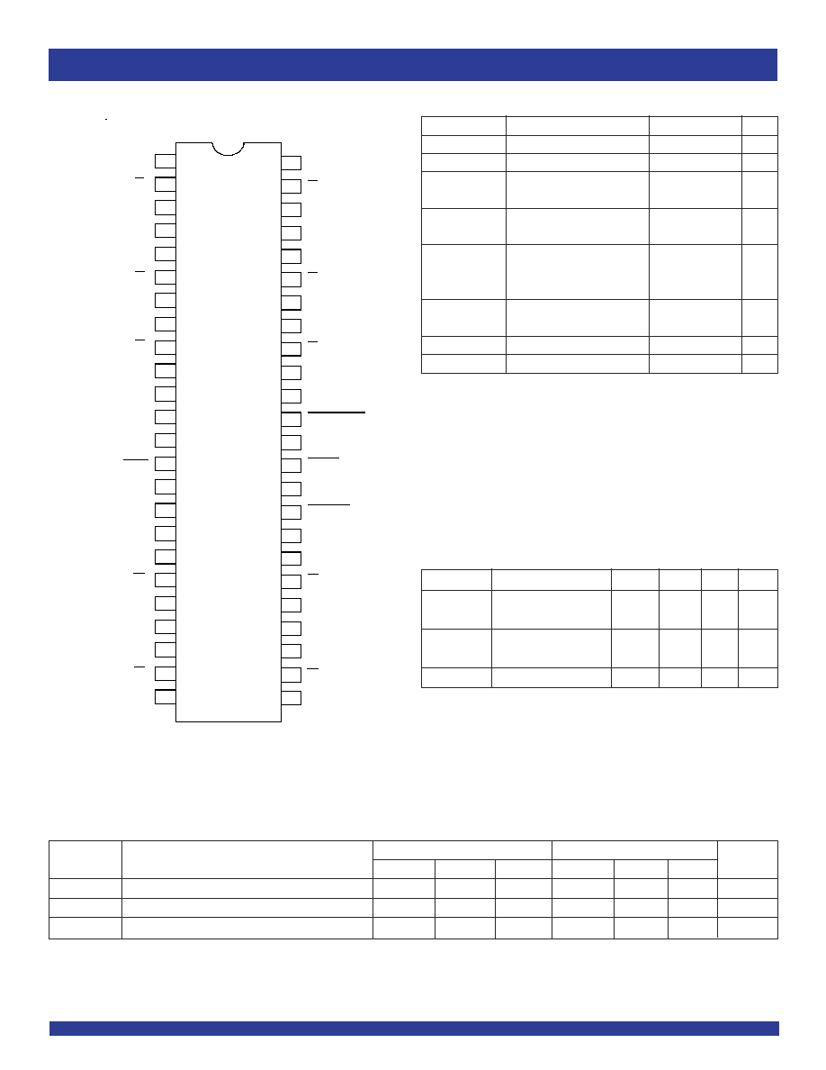
PIN CONFIGURATION
TSSOP
TOP VIEW
ABSOLUTE MAXIMUM RATINGS
(1)
Symbol
Rating
Max
Unit
V
DDQ
, AV
DD
Supply Voltage Range
≠0.5 to +3.6
V
V
I(2)
Input Voltage Range
≠0.5 to V
DDQ
+ 0.5
V
V
O(2)
Voltage range applied to any
≠0.5 to V
DDQ
+ 0.5
V
output in the high or low state
I
IK
Input Clamp Current
≠50
mA
(V
I
<0)
I
OK
Output Clamp Current
±50
mA
(V
O
<0 or
V
O
> V
DDQ
)
I
O
Continuous Output Current
±50
mA
(V
O
=0 to V
DDQ
)
V
DDQ
or GND
Continuous Current
±100
mA
TSTG
Storage Temperature Range
≠ 65 to +150
∞C
NOTES:
1. Stresses greater than those listed under ABSOLUTE MAXIMUM RATINGS may cause
permanent damage to the device. This is a stress rating only and functional operation
of the device at these or any other conditions above those indicated in the operational
sections of this specification is not implied. Exposure to absolute maximum rating
conditions for extended periods may affect reliability.
2. The input and output negative-voltage ratings may be exceeded if the input and output
clamp-current ratings are observed.
3. The maximum package power dissipation is calculated using a junction temperature
of 150
∞
C and a board trace length of 750 mils.
CAPACITANCE
(1)
Parameter
Description
Min.
Typ.
Max.
Unit
C
IN
Input Capacitance
2.5
--
3.5
pF
V
I
= V
DDQ
or GND
C
I(
)
Delta Input Capacitance
-0.25
--
0.25
pF
V
I
= V
DDQ
or GND
C
L
Load Capacitance
--
14
--
pF
NOTE:
1. Unused inputs must be held high or low to prevent them from floating.
RECOMMENDED OPERATING CONDITIONS
CSPT857
CSPT857A
Symbol
Parameter
Min.
Typ.
Max.
Min.
Typ.
Max.
Unit
AV
DD
Supply Voltage
V
DDQ
V
DDQ
≠ 0.12
V
DDQ
2.7
V
V
DDQ
I/O Supply Voltage
2.3
2.5
2.7
2.3
2.5
2.7
V
T
A
Operating Free-Air Temperature
-40
+85
0
+70
∞
C
4
COMMERCIAL AND INDUSTRIAL TEMPERATURE RANGES
IDTCSPT857/A
2.5V PLL DIFFERENTIAL 1:10 SDRAM CLOCK DRIVER
NOTES:
1. H = HIGH Voltage Level
L = LOW Voltage Level
Z = High-Impedance OFF-State
X = Don't Care
2. Additional feature that senses when the clock input is less than approximately 20MHz and places the part in sleep mode. Reciever inputs and PLL are turned off and outputs
= tristate.
FUNCTION TABLE
(1)
INPUTS
OUTPUTS
AV
DD
PWRDWN
CLK
CLK
Y
Y
FBOUT
FBOUT
PLL
GND
H
L
H
L
H
L
H
Bypassed/OFF
GND
H
H
L
H
L
H
L
Bypassed/OFF
X
L
L
H
Z
Z
Z
Z
OFF
X
L
H
L
Z
Z
Z
Z
OFF
2.5V (nom)
H
L
H
L
H
L
H
ON
2.5V (nom)
H
H
L
H
L
H
L
ON
2.5V (nom)
(2)
X
<20MHz
<20MHz
Z
Z
Z
Z
OFF
PIN DESCRIPTION (TSSOP)
Pin Name
Pin Number
Description
AGND
17
Ground for 2.5V analog supply
AV
DD
16
2.5V analog supply
CLK, CLK
13, 14
Differential clock input
FBIN, FBIN
35, 36
Feedback differential clock input
FBOUT, FBOUT
32, 33
Feedback differential clock output
GND
1, 7, 8, 18, 24, 25, 31, 41, 42, 48
Ground
PWRDWN
37
Output enable for Y and Y
V
DDQ
4, 11, 12, 15, 21, 28, 34, 38, 45
2.5V supply
Y
[0:9]
3, 5, 10, 20, 22, 27, 29, 39, 44, 46
Buffered output of input clock, CLK
Y
[0:9]
2, 6, 9, 19, 23, 26, 30, 40, 43, 47
Buffered output of input clock, CLK
PIN DESCRIPTION (VFBGA)
Pin Name
Pin Number
Description
AGND
H1
Ground for 2.5V analog supply
AV
DD
G2
2.5V analog supply
CLK, CLK
F1, F2
Differential clock input
FBIN, FBIN
F5, F6
Feedback differential clock input
FBOUT, FBOUT
H6, G5
Feedback differential clock output
GND
A3, A4, C1, C2, C5, C6, H2, H5, K3, K4
Ground
PWRDWN
E6
Output enable for Y and Y
V
DDQ
B3, B4, E1, E2, E5, G1, G6, J3, J4
2.5V supply
Y
[0:9]
A1, A6, B2, B5, D1, D6, J2, J5, K1, K6
Buffered output of input clock, CLK
Y
[0:9]
A2, A5, B1, B6, D2, D5, J1, J6, K2, K5
Buffered output of input clock, CLK
5
IDTCSPT857/A
2.5V PLL DIFFERENTIAL 1:10 SDRAM CLOCK DRIVER
COMMERCIAL AND INDUSTRIAL TEMPERATURE RANGES
DC ELECTRICAL CHARACTERISTICS OVER OPERATING RANGE
Following Conditions Apply Unless Otherwise Specified:
Commercial: T
A
= 0∞C to +70∞C; Industrial: T
A
= ≠40∞C to +85∞C
Symbol
Parameter
Conditions
Min.
Typ.
Max.
Unit
V
IK
Input Clamp Voltage (All Inputs)
V
DDQ
= 2.3V, I
I
= -18mA
≠ 1.2
V
V
IL (dc)
Static Input LOW Voltage
PWRDWN
≠ 0.3
0.7
V
V
IH (dc)
Static Input HIGH Voltage
PWRDWN
1.7
V
DDQ
+ 0.3
V
IL (ac)
Dynamic Input LOW Voltage
CLK, CLK, FBIN, FBIN
0.7
V
V
IH (ac)
Dynamic Input HIGH Voltage
CLK, CLK, FBIN, FBIN
1.7
V
DDQ
V
OL
Output LOW Voltage
A
VDD
/V
DDQ
= Min., I
OL
= 100
µA
0.1
V
A
VDD
/V
DDQ
= Min., I
OL
= 12mA
0.6
V
OH
Output HIGH Voltage
A
VDD
/V
DDQ
= Min., I
OH
= -100
µA
V
DDQ
≠ 0.1
V
A
VDD
/V
DDQ
= Min., I
OH
= -12mA
1.7
V
IX
Input Differential Cross Voltage
V
DDQ
/2 ≠ 0.2
V
DDQ
/2 + 0.2
V
V
ID(DC) (1)
DC Input Differential Voltage
0.36
V
DDQ
+ 0.6
V
V
ID(AC) (1)
AC Input Differential Voltage
0.7
V
DDQ
+ 0.6
V
I
IN
Input Current
V
DDQ
= 2.7V, V
I
= 0V to 2.7V
±10
µA
I
DDPD
Power-Down Current on V
DDQ
and A
VDD
A
VDD
/V
DDQ
= Max., CLK = 0MHz or PWRDWN = L
100
200
µA
I
DDQ
Dynamic Power Supply Current on V
DDQ
A
VDD
/V
DDQ
= Max., CLK = 200MHz, 120
/14pF
320
360
mA
A
VDD
/V
DDQ
= Max., CLK = 170MHz, 120
/14pF
250
300
I
ADD
Dynamic Power Supply Current on A
VDD
A
VDD
/V
DDQ
= Max., CLK = 170MHz
12
mA
NOTE:
1. V
ID
is the magnitude of the difference between the input level on CLK and the input level on CLK.