DATASHEET SEARCH SITE | WWW.ALLDATASHEET.COM
1
NOVEMBER 2003
IDT72V3654
IDT72V3664
IDT72V3674
3.3 VOLT CMOS SyncBiFIFO
TM
WITH BUS-MATCHING
2,048 x 36 x 2
4,096 x 36 x 2
8,192 x 36 x 2
IDT and the IDT logo are registered trademarks of Integrated Device Technology, Inc. The SyncFIFO is a trademark of Integrated Device Technology, Inc.
COMMERCIAL TEMPERATURE RANGE
2003 Integrated Device Technology, Inc. All rights reserved. Product specifications subject to change without notice.
DSC-4664/4
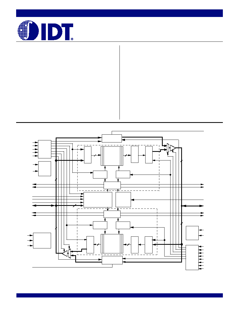
FUNCTIONAL BLOCK DIAGRAM
FEATURES
·
·
·
·
·
Memory storage capacity:
IDT72V3654
2,048 x 36 x 2
IDT72V3664
4,096 x 36 x 2
IDT72V3674
8,192 x 36 x 2
·
·
·
·
·
Clock frequencies up to 100 MHz (6.5ns access time)
·
·
·
·
·
Two independent clocked FIFOs buffering data in opposite
directions
·
·
·
·
·
Select IDT Standard timing (using
EFA, EFB, FFA, and FFB flags
functions) or First Word Fall Through Timing (using ORA, ORB,
IRA, and IRB flag functions)
·
·
·
·
·
Programmable Almost-Empty and Almost-Full flags; each has five
default offsets (8, 16, 64, 256 and 1,024 )
·
·
·
·
·
Serial or parallel programming of partial flags
·
·
·
·
·
Port B bus sizing of 36 bits (long word), 18 bits (word) and 9 bits
(byte)
·
·
·
·
·
Big- or Little-Endian format for word and byte bus sizes
·
·
·
·
·
Retransmit Capability
·
·
·
·
·
Master Reset clears data and configures FIFO, Partial Reset
clears data but retains configuration settings
·
·
·
·
·
Mailbox bypass registers for each FIFO
·
·
·
·
·
Free-running CLKA and CLKB may be asynchronous or coincident
(simultaneous reading and writing of data on a single clock edge
is permitted)
·
·
·
·
·
Auto power down minimizes power dissipation
·
·
·
·
·
Available in space saving 128-pin Thin Quad Flatpack (TQFP)
·
·
·
·
·
Pin and functionally compatible version of the 5V operating
IDT723654/723664/723674
·
·
·
·
·
Pin compatible to the lower density parts, IDT72V3624/72V3634/
72V3644
·
·
·
·
·
Industrial temperature range (40
°°
°°
°C to +85°°°°°C) is available
Mail 1
Register
Programmable Flag
Offset Registers
Input
Register
RAM ARRAY
2,048 x 36
4,096 x 36
8,192 x 36
Write
Pointer
Read
Pointer
Status Flag
Logic
Input
Register
Output
Register
RAM ARRAY
2,048 x 36
4,096 x 36
8,192 x 36
Write
Pointer
Read
Pointer
Status Flag
Logic
CLKA
CSA
W/
RA
ENA
MBA
Port-A
Control
Logic
FIFO1,
Mail1
Reset
Logic
MRS1
Mail 2
Register
MBF2
CLKB
CSB
W/RB
ENB
MBB
BE
BM
SIZE
Port-B
Control
Logic
FIFO2,
Mail2
Reset
Logic
MRS2
MBF1
FIFO1
FIFO2
13
EFB/ORB
AEB
36
36
FFB/IRB
AFB
B
0
-B
35
FFA/IRA
AFA
FS2
FS0/SD
FS1/
SEN
A
0
-A
35
EFA/ORA
AEA
4664 drw01
36
36
Output Bus-
Matching
Output
Register
PRS2
PRS1
Timing
Mode
FWFT
36
36
36
36
Input Bus-
Matching
FIFO1 and
FIFO2
Retransmit
Logic
RT1
RT2
RTM
2
COMMERCIAL TEMPERATURE RANGE
IDT72V3654/72V3664/72V3674 3.3V CMOS SyncBiFIFO
TM
WITH BUS-MATCHING
2,048 x 36 x 2, 4,096 x 36 x 2 and 8,192 x 36 x 2
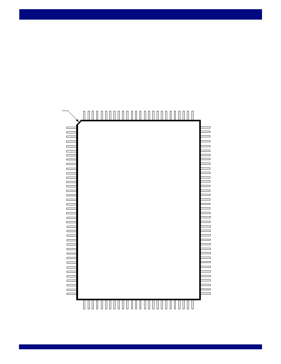
PIN CONFIGURATION
TQFP (PK128-1, order code: PF)
TOP VIEW
W/
RA
CLKB
4664 drw 02
1
2
3
4
5
6
7
8
9
10
11
12
13
14
15
16
17
18
19
20
21
22
23
24
25
26
27
28
29
30
31
32
33
34
35
36
37
38
ENA
CLKA
GND
A35
A34
A33
A32
Vcc
A31
A30
GND
A29
A28
A27
A26
A25
A24
A23
BE/
FWFT
GND
A22
Vcc
A21
A20
A19
A18
GND
A17
A16
A15
A14
A13
Vcc
A12
GND
A11
A10
39
40
41
42
43
44
45
46
47
48
49
50
51
52
53
54
55
56
57
58
59
60
61
62
63
64
65
66
67
68
69
70
71
72
73
74
75
76
77
78
79
80
81
82
83
84
85
86
87
88
89
90
91
92
93
94
95
96
97
98
99
100
102
101
128
127
126
125
124
123
122
121
120
119
118
117
116
115
114
113
112
111
110
109
108
107
106
105
PRS2/RT2
Vcc
B35
B34
B33
B32
RTM
GND
B31
B30
B29
B28
B27
B26
Vcc
B25
B24
BM
GND
B23
B22
B21
B20
B19
B18
GND
B17
B16
Vcc
B15
B14
B13
B12
GND
B11
B10
CSA
FFA
/IRA
EFA
/ORA
PRS1
/
RT1
Vcc
AFA
AEA
MBF2
MBA
MRS1
FS0/SD
GND
GND
FS1/
SEN
MRS2
MBB
MBF1
Vcc
AEB
AFB
EFB
/ORB
FFB
/IRB
GND
CSB
W
/RB
ENB
A9
A8
A7
A
6
G
N
D
A
5
A4
A3
Vcc
A2
A1
A0
GND
B0
B1
B2
B3
B4
B
5
GND
B
6
Vcc
B7
B8
B
9
104
103
INDEX
SIZE
FS2
DESCRIPTION
The IDT72V3654/72V3664/72V3674 are pin and functionally compat-
ible versions of the IDT723654/723664/723674, designed to run off a 3.3V
supply for exceptionally low-power consumption. These devices are mono-
lithic, high-speed, low-power, CMOS bidirectional synchronous (clocked)
FIFO memory which supports clock frequencies up to 100 MHz and has read
access times as fast as 6.5ns. Two independent 2,048/4,096/8,192 x 36 dual-
port SRAM FIFOs on board each chip buffer data in opposite directions. FIFO
data on Port B can be input and output in 36-bit, 18-bit, or 9-bit formats with a
choice of Big- or Little-Endian configurations.
These devices are a synchronous (clocked) FIFO, meaning each port
employs a synchronous interface. All data transfers through a port are gated
to the LOW-to-HIGH transition of a port clock by enable signals. The clocks for
each port are independent of one another and can be asynchronous or

3
COMMERCIAL TEMPERATURE RANGE
IDT72V3654/72V3664/72V3674 3.3V CMOS SyncBiFIFO
TM
WITH BUS-MATCHING
2,048 x 36 x 2, 4,096 x 36 x 2 and 8,192 x 36 x 2
coincident. The enables for each port are arranged to provide a simple
bidirectional interface between microprocessors and/or buses with synchro-
nous control.
Communication between each port may bypass the FIFOs via two mailbox
registers. The mailbox registers' width matches the selected Port B bus width.
Each Mailbox register has a flag (
MBF1 and MBF2) to signal when new mail
has been stored.
Two kinds of reset are available on these FIFOs: Master Reset and Partial
Reset. Master Reset initializes the read and write pointers to the first location
of the memory array, configures the FIFO for Big- or Little-Endian byte
arrangement and selects serial flag programming, parallel flag programming,
or one of five possible default flag offset settings, 8, 16, 64, 256 or 1,024. There
are two Master Reset pins,
MRS1 and MRS2.
Partial Reset also sets the read and write pointers to the first location of the
memory. Unlike Master Reset, any settings existing prior to Partial Reset (i.e.,
programming method and partial flag default offsets) are retained. Partial Reset
is useful since it permits flushing of the FIFO memory without changing any
configuration settings. Each FIFO has its own, independent Partial Reset pin,
PRS1 and PRS2.
Both FIFO's have Retramsmit capability, when a Retransmit is performed
on a respective FIFO only the read pointer is reset to the first memory location.
A Retransmit is performed by using the Retransmit Mode, RTM pin in conjunction
with the Retransmit pins
RT1 or RT2, for each respective FIFO. Note that the
two Retransmit pins
RT1 and RT2 are muxed with the Partial Reset pins.
These devices have two modes of operation: In the IDT Standard mode,
the first word written to an empty FIFO is deposited into the memory array. A
read operation is required to access that word (along with all other words
residing in memory). In the First Word Fall Through mode (FWFT), the first
word written to an empty FIFO appears automatically on the outputs, no read
operation required (Nevertheless, accessing subsequent words does neces-
sitate a formal read request). The state of the BE/
FWFT pin during Master
Reset determines the mode in use.
These devices have two modes of operation: In the IDT Standard mode,
the first word written to an empty FIFO is deposited into the memory array. A
read operation is required to access that word (along with all other words
residing in memory). In the First Word Fall Through mode (FWFT), the first long-
word (36-bit wide) written to an empty FIFO appears automatically on the
outputs, no read operation is required (Nevertheless, accessing subsequent
words does necessitate a formal read request). The state of the BE/
FWFT pin
during FIFO operation determines the mode in use.
Each FIFO has a combined Empty/Output Ready Flag (
EFA/ORA and
EFB/ORB) and a combined Full/Input Ready Flag (FFA/IRA and FFB/
IRB). The
EF and FF functions are selected in the IDT Standard mode. EF
indicates whether or not the FIFO memory is empty.
FF shows whether the
memory is full or not. The IR and OR functions are selected in the First Word
Fall Through mode. IR indicates whether or not the FIFO has available memory
locations. OR shows whether the FIFO has data available for reading or not.
It marks the presence of valid data on the outputs.
Each FIFO has a programmable Almost-Empty flag (
AEA and AEB)
and a programmable Almost-Full flag (
AFA and AFB). AEA and AEB
indicate when a selected number of words remain in the FIFO memory.
AFA
and
AFB indicate when the FIFO contains more than a selected number of
words.
FFA/IRA, FFB/IRB, AFA and AFB are two-stage synchronized to the
port clock that writes data into its array.
EFA/ORA, EFB/ORB, AEA and
AEB are two-stage synchronized to the port clock that reads data from its array.
Programmable offsets for
AEA, AEB, AFA and AFB are loaded in parallel
using Port A or in serial via the SD input. Five default offset settings are also
provided. The
AEA and AEB threshold can be set at 8, 16, 64, 256 or 1,024
locations from the empty boundary and the
AFA and AFB threshold can be
set at 8, 16, 64, 256 or 1,024 locations from the full boundary. All these choices
are made using the FS0, FS1 and FS2 inputs during Master Reset.
Interspersed Parity can also be selected during a Master Reset of the
FIFO. If Interspersed Parity is selected then during parallel programming of the
flag offset values, the device will ignore data line A8. If Non-Interspersed Parity
is selected then data line A8 will become a valid bit.
Two or more devices may be used in parallel to create wider data paths.
If, at any time, the FIFO is not actively performing a function, the chip will
automatically power down. During the power down state, supply current
consumption (I
CC
) is at a minimum. Initiating any operation (by activating control
inputs) will immediately take the device out of the power down state.
The IDT72V3654/72V3664/72V3674 are characterized for operation from
0
°C to 70°C. Industrial temperature range (-40°C to +85°C) is available. They
are fabricated using IDT's high speed, submicron CMOS technology.

4
COMMERCIAL TEMPERATURE RANGE
IDT72V3654/72V3664/72V3674 3.3V CMOS SyncBiFIFO
TM
WITH BUS-MATCHING
2,048 x 36 x 2, 4,096 x 36 x 2 and 8,192 x 36 x 2
PIN DESCRIPTIONS
Symbol
Name
I/O
Description
A0-A35
Port A Data
I/O
36-bit bidirectional data port for side A.
AEA
Port A Almost-
O
Programmable Almost-Empty flag synchronized to CLKA. It is LOW when the number of words in
Empty Flag
FIFO2 is less than or equal to the value in the Almost-Empty A Offset register, X2.
AEB
Port B Almost-
O
Programmable Almost-Empty flag synchronized to CLKB. It is LOW when the number of words in
Empty Flag
FIFO1 is less than or equal to the value in the Almost-Empty B Offset register, X1.
AFA
Port A Almost-
O
Programmable Almost-Full flag synchronized to CLKA. It is LOW when the number of empty
Full Flag
locations in FIFO1 is less than or equal to the value in the Almost-Full A Offset register, Y1.
AFB
Port B Almost-
O
Programmable Almost-Full flag synchronized to CLKB. It is LOW when the number of empty
Full Flag
locations in FIFO2 is less than or equal to the value in the Almost-Full B Offset register, Y2.
B0-B35
Port A Data
I/O
36-bit bidirectional data port for side B.
BE/
FWFT
Big-Endian/
I
This is a dual purpose pin. During Master Reset, a HIGH on BE will select Big Endian operation.
First Word
In this case, depending on the bus size, the most significant byte or word on Port A is read from
Fall Through
Port B first (A-to-B data flow) or written to Port B first (B-to-A data flow). A LOW on BE will select
Select
Little-Endian operation. In this case, the least significant byte or word on Port A is read from Port B
first (for A-to-B data flow) or written to Port B first (B-to-A data flow). After Master Reset, this pin
selects the timing mode. A HIGH on
FWFT selects IDT Standard mode, a LOW selects First Word
Fall Through mode. Once the timing mode has been selected, the level on
FWFT must be static
throughout device operation.
BM
(1)
Bus-Match Select
I
A HIGH on this pin enables either byte or word bus width on Port B, depending on the state of
(Port B)
SIZE. A LOW selects long word operation. BM works with SIZE and BE to select the bus size and
endian arrangement for Port B. The level of BM must be static throughout device operation.
CLKA
Port A Clock
I
CLKA is a continuous clock that synchronizes all data transfers through Port A and can be
asynchronous or coincident to CLKB.
FFA/IRA, EFA/ORA, AFA, and AEA are all synchronized
to the LOW-to-HIGH transition of CLKA.
CLKB
Port B Clock
I
CLKB is a continuous clock that synchronizes all data transfers through Port B and can be
asynchronous or coincident to CLKA.
FFB/IRB, EFB/ORB, AFB, and AEB are synchronized to
the LOW-to-HIGH transition of CLKB.
CSA
Port A Chip Select
I
CSA must be LOW to enable to LOW-to-HIGH transition of CLKA to read or write on Port A.
The A0-A35 outputs are in the high-impedance state when
CSA is HIGH.
CSB
Port B Chip Select
I
CSB must be LOW to enable a LOW-to-HIGH transition of CLKB to read or write data on Port B.
The B0-B35 outputs are in the high-impedance state when
CSB is HIGH.
EFA/ORA
Port A Empty/
O
This is a dual function pin. In the IDT Standard mode, the
EFA function is selected. EFA
Output Ready Flag
indicates whether or not the FIFO2 memory is empty. In the FWFT mode, the ORA function is
selected. ORA indicates the presence of valid data on A0-A35 outputs, available for reading.
EFA/ORA is synchronized to the LOW-to-HIGH transition of CLKA.
EFB/ORB
Port B Empty/
O
This is a dual function pin. In the IDT Standard mode, the
EFB function is selected. EFB indicates
Output Ready Flag
whether or not the FIFO1 memory is empty. In the FWFT mode, the ORB function is selected. ORB
indicates the presence of valid data on the B0-B35 outputs, available for reading.
EFB/ORB is
synchronized to the LOW-to-HIGH transition of CLKB.
ENA
Port A Enable
I
ENA must be HIGH to enable a LOW-to-HIGH transition of CLKA to read or write data on Port A.
ENB
Port B Enable
I
ENB must be HIGH to enable a LOW-to-HIGH transition of CLKB to read or write data on Port B.
FFA/IRA
Port A Full/
O
This is a dual function pin. In the IDT Standard mode, the
FFA function is selected. FFA indicates
Input Ready Flag
whether or not the FIFO1 memory is full. In the FWFT mode, the IRA function is selected. IRA
indicates whether or not there is space available for writing to the FIFO1 memory.
FFA/IRA is
synchronized to the LOW-to-HIGH transition of CLKA.
FFB/IRB
Port B Full/
O
This is a dual function pin. In the IDT Standard mode, the
FFB function is selected. FFB indicates
Input Ready Flag
whether or not the FIFO2 memory is full. In the FWFT mode, the IRB function is selected. IRB
indicates whether or not there is space available for writing to the FIFO2 memory.
FFB/IRB is
synchronized to the LOW-to-HIGH transition of CLKB.

5
COMMERCIAL TEMPERATURE RANGE
IDT72V3654/72V3664/72V3674 3.3V CMOS SyncBiFIFO
TM
WITH BUS-MATCHING
2,048 x 36 x 2, 4,096 x 36 x 2 and 8,192 x 36 x 2
Symbol
Name
I/O
Description
FS0/SD
Flag Offset Select 0/
I
FS1/
SEN and FS0/SD are dual-purpose inputs used for flag offset register programming. During
Serial Data
Master Reset, FS1/
SEN and FS0/SD, together with FS2, select the flag offset programming method
Three offset register programming methods are available: automatically load one of five preset values
(8, 16, 64, 256 or 1,024), parallel load from Port A, and serial load.
FS1/
SEN
Flag Offset Select 1/
I
Serial Enable,
When serial load is selected for flag offset register programming, FS1/
SEN is used as an enable
synchronous to the LOW-to-HIGH transition of CLKA. When FS1/
SEN is LOW, a rising edge on CLKA
FS2
(1)
Flag Offset Select 2
I
load the bit present on FS0/SD into the X and Y registers. The number of bit writes required to program
the offset registers is 44 for the IDT72V3654, 48 for the IDT72V3664, and 52 for the IDT72V3674.
The first bit write stores the Y-register (Y1) MSB and the last bit write stores the X-register (X2) LSB.
MBA
Port A Mailbox
I
A HIGH level on MBA chooses a mailbox register for a Port A read or write operation. When
Select
the A0-A35 outputs are active, a HIGH level on MBA selects data from the mail2 register for output
and a LOW level selects FIFO2 output register data for output.
MBB
Port B Mailbox
I
A HIGH level on MBB chooses a mailbox register for a Port B read or write operation. When the
Select
B0-B35 outputs are active, a HIGH level on MBB selects data from the mail1 register for output and
a LOW level selects FIFO1 output register data for output.
MBF1
Mail1 Register
O
MBF1 is set LOW by a LOW-to-HIGH transition of CLKA that writes data to the mail1 register.
Flag
Writes to the mail1 register are inhibited while
MBF1 is LOW. MBF1 is set HIGH by a LOW-to-HIGH
transition of CLKB when a Port B read is selected and MBB is HIGH.
MBF1 is set HIGH following either
a Master or Partial Reset of FIFO1.
MBF2
Mail2 Register
O
MBF2 is set LOW by a LOW-to-HIGH transition of CLKB that writes data to the mail2 register. Writes
Flag
to the mail2 register are inhibited while
MBF2 is LOW. MBF2 is set HIGH by a LOW-to-HIGH
transition of CLKA when a Port A read is selected and MBA is HIGH.
MBF2 is set HIGH following
either a Master or Partial Reset of FIFO2.
MRS1
FIFO1 Master
I
A LOW on this pin initializes the FIFO1 read and write pointers to the first location of memory and sets the
Reset
Port B output register to all zeroes. A LOW-to-HIGH transition on
MRS1 selects the programming
method (serial or parallel) and one of five programmable flag default offsets for FIFO1 and FIFO2. It
also configures Port B for bus size and endian arrangement. Four LOW-to-HIGH transitions of CLKA
and four LOW-to-HIGH transitions of CLKB must occur while
MRS1 is LOW.
MRS2
FIFO2 Master
I
A LOW on this pin initializes the FIFO2 read and write pointers to the first location of memory and sets
Reset
the Port A output register to all zeroes. A LOW-to-HIGH transition on
MRS2, toggled simultaneously with
MRS1, selects the programming method (serial or parallel) and one of the programmable flag default
offsets for FIFO2. Four LOW-to-HIGH transitions of CLKA and four LOW-to-HIGH transitions of CLKB
must occur while
MRS2 is LOW.
PRS1/
Partial Reset/
I
This pin is muxed for both Partial Reset and Retransmit operations, it is used in conjunction with the RTM
RT1
Retransmit FIFO1
pin. If RTM is in a LOW condition, a LOW on this pin performs a Partial Reset on FIFO1 and initializes
the FIFO1 read and write pointers to the first location of memory and sets the Port B output register to
all zeroes. During Partial Reset, the currently selected bus size, endian arrangement, programming
method (serial or parallel), and programmable flag settings are all retained. If RTM is HIGH, a LOW on
this pin performs a Retransmit and initializes the FIFO1 read pointer only to the first memory location.
PRS2/
Partial Reset/
I
This pin is muxed for both Partial Reset and Retransmit operations, it is used in conjunction with the RTM
RT2
Retransmit FIFO2
pin. If RTM
is in a LOW condition, a LOW on this pin performs a Partial Reset on FIFO2 and initializes
the FIFO2 read and write selected bus size, endian arrangement, programming method (serial or
parallel), and programmable flag settings are all retained. If RTM is HIGH, a LOW on this pin performs
a Retransmit and initializes the FIFO2 read pointer only to the first memory location.
RTM
Retransmit Mode
I
This pin is used in conjunction with the
RT1 and RT2 pins. When RTM is HIGH a Retransmit is performed
on FIFO1 or FIFO2 respectively.
SIZE
(1)
Bus Size Select
I
A HIGH on this pin when BM is HIGH selects byte bus (9-bit) size on Port B. A LOW on this pin when
BM is HIGH selects word (18-bit) bus size. SIZE works with BM and BE to select the bus size and endian
arrangement for Port B. The level of SIZE must be static throughout device operation
PIN DESCRIPTIONS (CONTINUED)
NOTE:
1. FS2, BM and SIZE inputs are not TTL compatible. These inputs should be tied to GND or V
CC
.