1
IDT74FCT841AT/BT/CT/DT
FAST CMOS BUS INTERFACE LATCH
COMMERCIAL TEMPERATURE RANGE
SEPTEMBER 1999
1999 Integrated Device Technology, Inc.
DSC-2571/7
c
IDT74FCT841AT/BT/CT/DT
COMMERCIAL TEMPERATURE RANGE
FAST CMOS BUS
INTERFACE LATCH
DESCRIPTION:
The FCT841T series is built using an advanced dual metal CMOS
technology.
The FCT841T bus interface latches are designed to eliminate the extra
packages required to buffer existing latches and provide extra data width
for wider address/data paths or buses carrying parity. The FCT841T are
buffered, 10-bit wide versions of the popular FCT373T function. They are
ideal for use as an output port requiring high I
OL
/I
OH
.
All of the FCT841T high-performance interface family can drive large
capacitive loads, while providing low-capacitance bus loading at both inputs
and outputs. All inputs have clamp diodes to ground and all outputs are
designed for low-capacitance bus loading in high-impedance state.
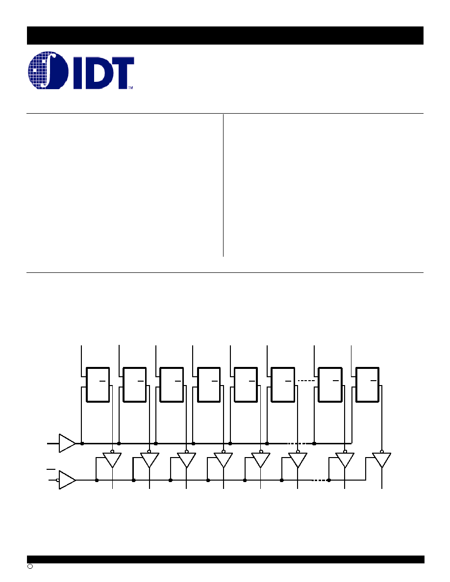
FUNCTIONAL BLOCK DIAGRAM
D
0
D
Y
0
LE Q
LE
OE
D
1
D
Y
1
LE Q
D
2
D
Y
2
LE
Q
D
3
D
Y
3
LE Q
D
4
D
Y
4
LE
Q
D
5
D
Y
5
LE
Q
D
8
D
Y
8
LE
Q
D
9
D
Y
9
LE
Q
FEATURES:
-
Low input and output leakage
1µ A (max.)
-
Extended commercial range of ≠40∞C to +85∞C
-
CMOS power levels
-
True TTL input and output compatibility
∑
V
OH
= 3.3V (typ.)
∑
V
OL
= 0.3V (typ.)
-
Meets or exceeds JEDEC standard 18 specifications
-
Product available in Radiation Tolerant and Radiation Enhanced
versions
-
Available in PDIP, SOIC, SSOP, and QSOP packages
-
A, B, C and D speed grades
-
High drive outputs (-15mA I
OH
, 48mA I
OL
)
-
Power off disable outputs permit "live insertion"
2
COMMERCIAL TEMPERATURE RANGE
IDT74FCT841AT/BT/CT/DT
FAST CMOS BUS INTERFACE LATCH
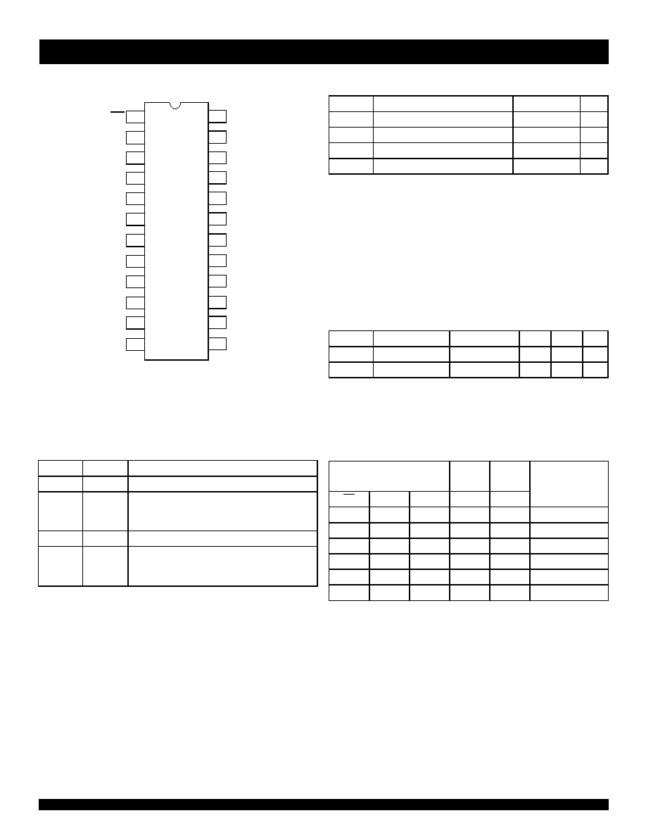
PIN CONFIGURATION
PDIP/ SOIC/ SSOP/ QSOP
TOP VIEW
2
3
1
20
19
18
15
16
9
10
D
6
D
7
D
2
D
5
D
3
D
4
D
8
23
22
24
21
17
5
6
7
4
P24-1
D24-1
SO 24-2
SO 24-7
SO 24-8
8
D
0
V
CC
LE
OE
13
14
11
12
D
1
GN D
D
9
Y
6
Y
7
Y
2
Y
5
Y
3
Y
4
Y
8
Y
0
Y
1
Y
9
NOTE:
1. H = HIGH
L = LOW
X = Don't Care
NC = No Change
Z = High-Impedance
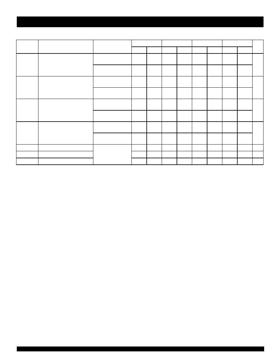
PIN DESCRIPTION
Name
I/O
Description
D
I
I
The latch data inputs.
LE
I
The latch enable input. The latches are transparent
when LE is HIGH. Input data is latched on the HIGH-
to-LOW transition.
Y
I
O
The 3-state latch outputs.
OE
I
The output enable control. When
OE is LOW, the
outputs are enabled. When
OE is HIGH, the outputs
VI
are in high-impedance (off) state.
FUNCTION TABLE
(1)
Inputs
Internal
Output
OE
LE
D
I
Q
I
Y
I
Function
H
H
L
L
Z
High Z
H
H
H
H
Z
High Z
H
L
X
NC
Z
Latched (High Z)
L
H
L
L
L
Transparent
L
H
H
H
H
Transparent
L
L
X
NC
NC
Latched
ABSOLUTE MAXIMUM RATINGS
(1)
Symbol
Rating
Max.
Unit
V
TERM(2)
Terminal Voltage with Respect to GND
≠0.5 to +7
V
V
TERM(3)
Terminal Voltage with Respect to GND
≠0.5 to V
CC
+0.5
V
T
STG
Storage Temperature
≠65 to +150
∞C
I
OUT
DC Output Current
≠65 to +120
mA
8T-link
NOTES:
1. Stresses greater than those listed under ABSOLUTE MAXIMUM
RATINGS may cause permanent damage to the device. This is a
stress rating only and functional operation of the device at these or
any other conditions above those indicated in the operational sections
of this specification is not implied. Exposure to absolute maximum
rating conditions for extended periods may affect reliability. No
terminal voltage may exceed Vcc by +0.5V unless otherwise noted.
2. Inputs and Vcc terminals only.
3. Outputs and I/O terminals only.
CAPACITANCE (T
A
= +25
O
C, f = 1.0MHz)
Symbol
Parameter
(1)
Conditions
Typ.
Max.
Unit
C
IN
Input Capacitance
V
IN
= 0V
6
10
pF
C
OUT
Output Capacitance
V
OUT
= 0V
8
12
pF
8T-link
NOTE:
1. This parameter is measured at characterization but not tested.
3
IDT74FCT841AT/BT/CT/DT
FAST CMOS BUS INTERFACE LATCH
COMMERCIAL TEMPERATURE RANGE
NOTES:
1. For conditions shown as Max. or Min., use appropriate value specified under Electrical Characteristics for the applicable device type.
2. Typical values are at Vcc = 5.0V, +25∞C ambient.
3. Not more than one output should be shorted at one time. Duration of the short circuit test should not exceed one second.
4. The test limit for this parameter is ±5µA at T
A
= ≠55∞C.
5. This parameter is guaranteed but not tested.
DC ELECTRICAL CHARACTERISTICS OVER OPERATING RANGE
Following Conditions Apply Unless Otherwise Specified:
Commercial: T
A
= ≠40∞C to +85∞C, V
CC
= 5.0V ± 5%
Symbol
Parameter
Test Conditions
(1)
Min.
Typ.
(2)
Max.
Unit
V
IH
Input HIGH Level
Guaranteed Logic HIGH Level
2
--
--
V
V
IL
Input LOW Level
Guaranteed Logic LOW Level
--
--
0.8
V
I
I H
Input HIGH Current
(4)
V
CC
= Max.
V
I
= 2.7V
--
--
±1
µ A
I
I L
Input LOW Current
(4)
V
I
= 0.5V
--
--
±1
I
OZH
High Impedance Output Current
V
CC
= Max.
V
O
= 2.7V
--
--
±1
µ A
I
OZL
(3-State Output Pins)
(4)
V
O
= 0.5V
--
--
±1
I
I
Input HIGH Current
(4)
V
CC
= Max., V
I
= V
CC
(Max.)
--
--
±1
µ A
V
IK
Clamp Diode Voltage
V
CC
= Min., I
IN
= ≠18mA
--
≠0.7
≠1.2
V
V
H
Input Hysteresis
--
--
200
--
mV
I
CC
Quiescent Power Supply Current
V
CC
= Max., V
IN
=
GND or
V
CC
--
0.01
1
mA
OUTPUT DRIVE CHARACTERISTICS
Symbol
Parameter
Test Conditions
(1)
Min.
Typ.
(2)
Max.
Unit
V
OH
Output HIGH Voltage
V
CC
= Min.
I
OH
= ≠8mA
2.4
3.3
--
V
V
IN
=
V
IH
or
V
IL
I
OH
= ≠15mA
2
3
--
V
OL
Output LOW Voltage
V
CC
= Min.
I
OL
= 48mA
--
0.3
0.5
V
V
IN
=
V
IH
or
V
IL
I
OS
Short Circuit Current
V
CC
= Max., V
O
= GND
(3)
≠60
≠120
≠225
mA
I
OFF
Input/Output Power Off Leakage
(5)
V
CC
= 0V, V
IN
or V
O
4.5V
--
--
±
1
µ A
4
COMMERCIAL TEMPERATURE RANGE
IDT74FCT841AT/BT/CT/DT
FAST CMOS BUS INTERFACE LATCH
POWER SUPPLY CHARACTERISTICS
Symbol
Parameter
Test Conditions
(1)
Min.
Typ.
(2)
Max.
Unit
I
CC
Quiescent Power Supply Current
TTL Inputs HIGH
V
CC
= Max.
V
IN
= 3.4V
(3)
--
0.5
2
mA
I
CCD
Dynamic Power Supply Current
(4)
V
CC
= Max.
Outputs Open
OE = GND
V
IN
= V
CC
V
IN
= GND
--
0.15
0.25
mA/
MHz
LE = V
CC
One Input Toggling
50% Duty Cycle
I
C
Total Power Supply Current
(6)
V
CC
= Max.
V
IN
= V
CC
--
1.5
3.5
mA
Outputs Open
fi = 10MHz
V
IN
= GND
50% Duty Cycle
OE
=
GND
V
IN
= 3.4
V
IN
= GND
--
1.8
4.5
LE = V
CC
One Bit Toggling
V
CC
= Max.
V
IN
= V
CC
--
3
6
(5)
Outputs Open
fi = 2.5MHz
V
IN
= GND
50% Duty Cycle
OE
=
GND
V
IN
= 3.4
V
IN
= GND
--
5
14
(5)
LE = V
CC
Eight Bits Toggling
NOTES:
1. For conditions shown as Max. or Min., use appropriate value specified under Electrical Characteristics for the applicable device type.
2. Typical values are at V
CC
= 5.0V, +25∞C ambient.
3. Per TTL driven input (V
IN
= 3.4V). All other inputs at V
CC
or GND.
4. This parameter is not directly testable, but is derived for use in Total Power Supply Calculations.
5. Values for these conditions are examples of the I
CC
formula. These limits are guaranteed but not tested.
6. I
C
= I
QUIESCENT
+ I
INPUTS
+ I
DYNAMIC
I
C
= I
CC
+
I
CC
D
H
N
T
+ I
CCD
(f
CP/
2 + f
i
N
i
)
I
CC
= Quiescent Current
I
CC
= Power Supply Current for a TTL High Input (V
IN
= 3.4V)
D
H
= Duty Cycle for TTL Inputs High
N
T
= Number of TTL Inputs at D
H
I
CCD
= Dynamic Current Caused by an Input Transition Pair (HLH or LHL)
f
CP
= Clock Frequency for Register Devices (Zero for Non-Register Devices)
f
i
= Input Frequency
N
i
= Number of Inputs at f
i
All currents are in milliamps and all frequencies are in megahertz.
5
IDT74FCT841AT/BT/CT/DT
FAST CMOS BUS INTERFACE LATCH
COMMERCIAL TEMPERATURE RANGE
NOTES:
1. See test circuit and waveforms.
2. Minimum limits are guaranteed but not tested on Propagation Delays.
3. These parameters are guaranteed but not tested.
4. These conditions are guaranteed but not tested.
SWITCHING CHARACTERISTICS OVER OPERATING RANGE
FCT841AT
FCT841BT
FCT841CT
FCT841DT
Symbol
Parameter
Conditions
(1)
Min.
(2)
Max.
Min.
(2)
Max.
Min.
(2)
Max.
Min.
(2)
Max.
Unit
t
PLH
t
PHL
Propagation Delay
D
I
to
Y
I
(LE = HIGH)
C
L
= 50pF
R
L
= 500
1.5
9
1.5
6.5
1.5
5.5
1.5
4.2
ns
C
L
= 300pF
(4)
R
L
= 500
1.5
13
1.5
13
1.5
13
1.5
8
t
PLH
t
PHL
Propagation Delay
LE to
Y
I
C
L
= 50pF
R
L
= 500
1.5
12
1.5
8
1.5
6.4
1.5
4
ns
C
L
= 300pF
(4)
R
L
= 500
1.5
16
1.5
15.5
1.5
15
1.5
8
t
PZH
t
PZL
Output Enable Time
OE to Y
I
C
L
= 50pF
R
L
= 500
1.5
11.5
1.5
8
1.5
6.5
1.5
4.8
ns
C
L
= 300pF
(4)
R
L
= 500
1.5
23
1.5
14
1.5
12
1.5
9
t
PHZ
t
PLZ
Output Disable Time
OE to Y
I
C
L
= 5pF
(4)
R
L
= 500
1.5
7
1.5
6
1.5
5.7
1.5
4
ns
C
L
= 50pF
R
L
= 500
1.5
8
1.5
7
1.5
6
1.5
4
t
SU
Data to LE Set-up Time
C
L
= 50pF
2.5
--
2.5
--
2.5
--
1.5
--
ns
t
H
Data to LE Hold Time
R
L
= 500
2.5
--
2.5
--
2.5
--
1
--
ns
t
W
LE Pulse Width HIGH
(3)
4
--
4
--
4
--
3
--
ns
6
COMMERCIAL TEMPERATURE RANGE
IDT74FCT841AT/BT/CT/DT
FAST CMOS BUS INTERFACE LATCH
Pulse
Generator
R
T
D.U.T.
V
CC
V
IN
C
L
V
OUT
50pF
500
500
7.0V
3V
1.5V
0V
3V
1.5V
0V
3V
1.5V
0V
3V
1.5V
0V
DATA
IN PU T
TIM IN G
IN PU T
ASYN CH R ON OUS C ON TROL
PRES ET
CLEAR
ETC.
SYNC HRO N OU S CON TRO L
t
SU
t
H
t
REM
t
SU
t
H
HIGH-LOW -HIGH
PULSE
LO W -H IGH -LOW
PULSE
t
W
1.5V
1.5V
SAM E PHASE
IN PU T TR ANSITION
3V
1.5V
0V
1.5V
V
OH
t
PLH
OU TPUT
OPPOSITE P HASE
IN PU T TR ANSITION
3V
1.5V
0V
t
PLH
t
PH L
t
PH L
V
OL
CO NTR OL
IN PU T
3V
1.5V
0V
3.5V
0V
OU TPUT
NO RM A LLY
LO W
OU TPUT
NO RM A LLY
HIGH
SW ITC H
CLOSE D
SW ITC H
OPEN
V
OL
0.3V
0.3V
t
PLZ
t
PZL
t
PZH
t
PHZ
3.5V
0V
1.5V
1.5V
ENAB LE
DISA BLE
V
OH
PRES ET
CLEAR
CLOC K ENABLE
ETC.
O ctal lin k
O ctal lin k
O ctal lin k
O ctal lin k
O ctal lin k
TEST CIRCUITS AND WAVEFORMS
PROPAGATION DELAY
TEST CIRCUITS FOR ALL OUTPUTS
ENABLE AND DISABLE TIMES
SET-UP, HOLD, AND RELEASE TIMES
PULSE WIDTH
NOTES:
1. Diagram shown for input Control Enable-LOW and input Control Disable-
HIGH
2. Pulse Generator for All Pulses: Rate
1.0MHz; t
F
2.5ns; t
R
2.5ns
SWITCH POSITION
Test
Switch
Open Drain
Disable Low
Closed
Enable Low
All Other Tests
Open
8-link
DEFINITIONS:
C
L
= Load capacitance: includes jig and probe capacitance.
R
T
= Termination resistance: should be equal to Z
OUT
of the Pulse
Generator.
7
IDT74FCT841AT/BT/CT/DT
FAST CMOS BUS INTERFACE LATCH
COMMERCIAL TEMPERATURE RANGE
CORPORATE HEADQUARTERS
for SALES:
2975 Stender Way
800-345-7015 or 408-727-6116
Santa Clara, CA 95054
fax: 408-492-8674
www.idt.com*
*To search for sales office near you, please click the sales button found on our home page or dial the 800# above and press 2.
The IDT logo is a registered trademark of Integrated Device Technology, Inc.
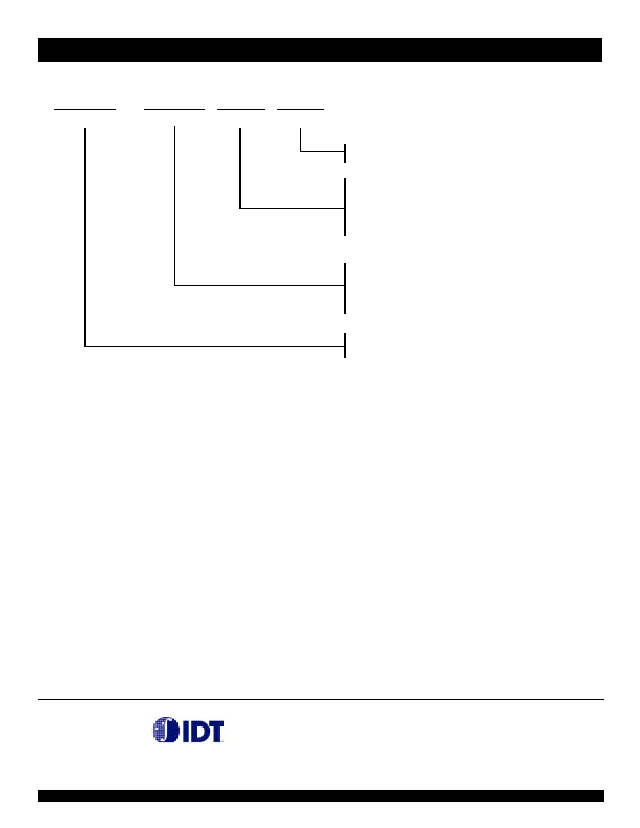
ORDERING INFORMATION
ID T XX
Tem p. R ange
XXXX
D evice Type
X
Package
X
Process
Blank
P
D
SO
PY
Q
841AT
841BT
841C T
841D T
C om m ercial
Plastic D IP (P24-1)
C ER D IP (D 24-1)
Sm all Outline IC (SO 24-2)
Shrink Sm a ll O utline P ackage (SO24-7)
Quarter-size S m all O u tline Package (S O24-8)
10-Bit N on-Inverting Latch
74
- 40∞C to +8 5∞C
FC T