Äîêóìåíòàöèÿ è îïèñàíèÿ www.docs.chipfind.ru
1
COMMERCIAL AND INDUSTRIAL TEMPERATURE RANGES
IDT2308A
3.3V ZERO DELAY CLOCK MULTIPLIER
JULY 2004
2004 Integrated Device Technology, Inc.
DSC 6587/8
c
COMMERCIAL AND INDUSTRIAL TEMPERATURE RANGES
The IDT logo is a registered trademark of Integrated Device Technology, Inc.
FEATURES:
· Phase-Lock Loop Clock Distribution for Applications ranging
from 10MHz to 133MHz operating frequency
· Distributes one clock input to two banks of four outputs
· Separate output enable for each output bank
· External feedback (FBK) pin is used to synchronize the outputs
to the clock input
· Output Skew <200 ps
· Low jitter <200 ps cycle-to-cycle
· 1x, 2x, 4x output options (see table):
IDT2308A-1 1x
IDT2308A-2 1x, 2x
IDT2308A-3 2x, 4x
IDT2308A-4 2x
IDT2308A-1H and -2H for High Drive
· No external RC network required
· Operates at 3.3V V
DD
· Available in SOIC and TSSOP packages
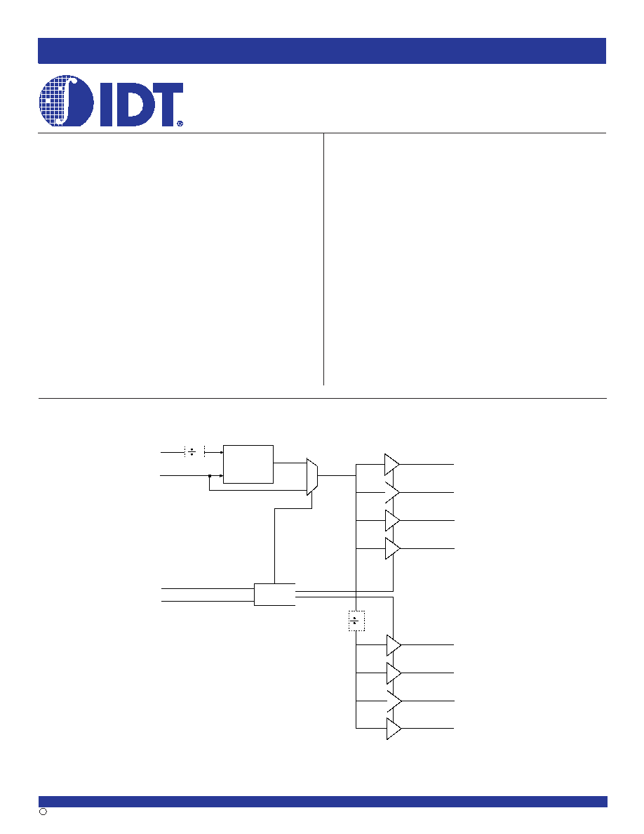
FUNCTIONAL BLOCK DIAGRAM
DESCRIPTION:
The IDT2308A is a high-speed phase-lock loop (PLL) clock multiplier. It is
designed to address high-speed clock distribution and multiplication applica-
tions. The zero delay is achieved by aligning the phase between the incoming
clock and the output clock, operable within the range of 10 to 133MHz.
The IDT2308A has two banks of four outputs each that are controlled via two
select addresses. By proper selection of input addresses, both banks can be
put in tri-state mode. In test mode, the PLL is turned off, and the input clock
directly drives the outputs for system testing purposes. In the absence of an
input clock, the IDT2308A enters power down. In this mode, the device will
draw less than 12µA for Commercial Temperature range and less than 25µA
for Industrial temperature range, and the outputs are tri-stated.
The IDT2308A is available in six unique configurations for both pre-
scaling and multiplication of the Input REF Clock. (See available options
table.)
The PLL is closed externally to provide more flexibility by allowing the user
to control the delay between the input clock and the outputs.
The IDT2308A is characterized for both Industrial and Commercial opera-
tion.
IDT2308A
3.3V ZERO DELAY CLOCK
MULTIPLIER
PLL
S1
2
14
15
3
CLKA1
CLKA2
CLKA3
CLKA4
6
10
11
CLKB1
CLKB2
CLKB3
CLKB4
9
FBK
16
Control
Logic
7
8
1
REF
S2
(-2, -3)
(-3, -4)
2
2
2
COMMERCIAL AND INDUSTRIAL TEMPERATURE RANGES
IDT2308A
3.3V ZERO DELAY CLOCK MULTIPLIER
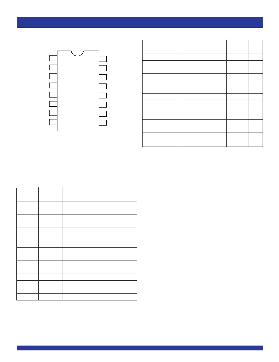
PIN CONFIGURATION
SOIC/ TSSOP
TOP VIEW
REF
CLKA1
S2
2
3
4
5
6
7
8
9
10
11
12
13
14
15
16
1
CLKA2
GND
CLKB1
FBK
CLKA4
GND
S1
V
DD
V
DD
CLKB2
CLKB3
CLKB4
CLKA3
Symbol
Rating
Max.
Unit
V
DD
Supply Voltage Range
0.5 to +4.6
V
V
I (2)
Input Voltage Range (REF)
0.5 to +5.5
V
V
I
Input Voltage Range
0.5 to
V
(except REF)
V
DD
+0.5
I
IK
(V
I
< 0)
Input Clamp Current
50
mA
I
O
Continuous Output Current
±50
mA
(V
O
= 0 to V
DD
)
V
DD
or GND
Continuous Current
±100
mA
T
A
= 55°C
Maximum Power Dissipation
0.7
W
(in still air)
(3)
T
STG
Storage Temperature Range
65 to +150
°C
Operating
Commercial Temperature
0 to +70
°C
Temperature
Range
Operating
Industrial Temperature
-40 to +85
°C
Temperature
Range
NOTES:
1. Stresses greater than those listed under ABSOLUTE MAXIMUM RATINGS may
cause permanent damage to the device. This is a stress rating only and functional
operation of the device at these or any other conditions above those indicated in the
operational sections of this specification is not implied. Exposure to absolute maximum
rating conditions for extended periods may affect reliability.
2. The input and output negative-voltage ratings may be exceeded if the input and output
clamp-current ratings are observed.
3. The maximum package power dissipation is calculated using a junction temperature
of 150
°
C and a board trace length of 750 mils.
APPLICATIONS:
· SDRAM
· Telecom
· Datacom
· PC Motherboards/Workstations
· Critical Path Delay Designs
Pin Number
Functional Description
REF
(1)
1
Input Reference Clock, 5 Volt Tolerant Input
CLKA1
(2)
2
Clock Output for Bank A
CLKA2
(2)
3
Clock Output for Bank A
V
DD
4
3.3V Supply
GND
5
Ground
CLKB1
(2)
6
Clock Output for Bank B
CLKB2
(2)
7
Clock Output for Bank B
S2
(3)
8
Select Input, Bit 2
S1
(3)
9
Select Input, Bit 1
CLKB3
(2)
10
Clock Output for Bank B
CLKB4
(2)
11
Clock Output for Bank B
GND
12
Ground
V
DD
13
3.3V Supply
CLKA3
(2)
14
Clock Output for Bank A
CLKA4
(2)
15
Clock Output for Bank A
FBK
16
PLL Feedback Input
NOTES:
1. Weak pull down.
2. Weak pull down on all outputs.
3. Weak pull ups on these inputs.
PIN DESCRIPTION
ABSOLUTE MAXIMUM RATINGS
(1)
3
COMMERCIAL AND INDUSTRIAL TEMPERATURE RANGES
IDT2308A
3.3V ZERO DELAY CLOCK MULTIPLIER
Device
Feedback From
Bank A Frequency
Bank B Frequency
IDT2308A-1
Bank A or Bank B
Reference
Reference
IDT2308A-1H
Bank A or Bank B
Reference
Reference
IDT2308A-2
Bank A
Reference
Reference/2
IDT2308A-2
Bank B
2 x Reference
Reference
IDT2308A-2H
Bank A
Reference
Reference/2
IDT2308A-2H
Bank B
2 x Reference
Reference
IDT2308A-3
Bank A
2 x Reference
Reference or Reference
(1)
IDT2308A-3
Bank B
4 x Reference
2 x Reference
IDT2308A-4
Bank A or Bank B
2 x Reference
2 x Reference
NOTE:
1. Output phase is indeterminant (0° or 180° from input clock).
AVAILABLE OPTIONS FOR IDT2308A
S2
S1
CLK A
CLK B
Output Source
PLL Shut Down
L
L
Tri-State
Tri-State
PLL
Y
L
H
Driven
Tri-State
PLL
N
H
L
Driven
Driven
REF
Y
H
H
Driven
Driven
PLL
N
FUNCTION TABLE
(1)
SELECT INPUT DECODING
NOTE:
1. H = HIGH Voltage Level
L = LOW Voltage Level
ZERO DELAY AND SKEW CONTROL
To close the feedback loop of the IDT2308A, the FBK pin can be driven from any of the eight available output pins. The output driving the FBK pin
will be driving a total load of 7pF plus any additional load that it drives. The relative loading of this output (with respect to the remaining outputs) can adjust
the input-output delay.
For applications requiring zero input-output delay, all outputs including the one providing feedback should be equally loaded. Ensure the outputs are
loaded equally, for zero output-output skew.
4
COMMERCIAL AND INDUSTRIAL TEMPERATURE RANGES
IDT2308A
3.3V ZERO DELAY CLOCK MULTIPLIER
DC ELECTRICAL CHARACTERISTICS - COMMERCIAL
Symbol
Parameter
Conditions
Min.
Typ.
(1)
Max.
Unit
V
IL
Input LOW Voltage Level
--
--
0.8
V
V
IH
Input HIGH Voltage Level
2
--
--
V
I
IL
Input LOW Current
V
IN
= 0V
--
--
50
µA
I
IH
Input HIGH Current
V
IN
= V
DD
--
--
100
µA
V
OL
Output LOW Voltage
I
OL
= 8mA (-1, -2, -3, -4)
--
--
0.4
V
I
OL
= 12mA (-1H, -2H)
V
OH
Output HIGH Voltage
I
OH
= -8mA (-1, -2, -3, -4)
2.4
--
--
V
I
OH
= -12mA (-1H, -2H)
I
DD_PD
Power Down Current
REF = 0MHz (S2 = S1 = H)
--
--
12
µA
100MHz CLKA (-1, -2, -3, -4)
--
--
45
100MHz CLKA (-1H, -2H)
--
--
70
I
DD
Supply Current
Unloaded Outputs
66MHz CLKA (-1, -2, -3, -4)
--
--
32
mA
Select Inputs at V
DD
or GND
66MHz CLKA (-1H, -2H)
--
--
50
33MHz CLKA (-1, -2, -3, -4)
--
--
18
33MHz CLKA (-1H, -2H)
--
--
30
NOTE:
1. Applies to both REF and FBK.
Symbol
Parameter
Test Conditions
Min.
Max.
Unit
V
DD
Supply Voltage
3
3.6
V
T
A
Operating Temperature (Ambient Temperature)
0
70
°
C
C
L
Load Capacitance below 100MHz
--
30
pF
Load Capacitance from 100MHz to 133MHz
--
15
pF
C
IN
Input Capacitance
(1)
--
7
pF
OPERATING CONDITIONS- COMMERCIAL
5
COMMERCIAL AND INDUSTRIAL TEMPERATURE RANGES
IDT2308A
3.3V ZERO DELAY CLOCK MULTIPLIER
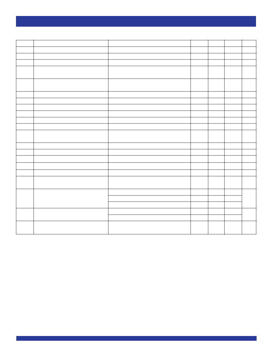
SWITCHING CHARACTERISTICS - COMMERCIAL
Symbol
Parameter
Conditions
Min.
Typ.
Max.
Unit
t
1
Output Frequency
30pF Load, all devices
10
--
100
MHz
t
1
Output Frequency
20pF Load, -1H, -2H Devices
10
--
133.3
MHz
t
1
Output Frequency
15pF Load, -1, -2, -3, -4 devices
10
--
133.3
MHz
Duty Cycle = t
2
÷ t
1
Measured at 1.4V, F
OUT
= 66.66MHz
40
50
60
%
(-1, -2, -3, -4, -1H, -2H)
30pF Load
Duty Cycle = t
2
÷ t
1
Measured at 1.4V, F
OUT
= 50MHz
45
50
55
%
(-1, -2, -3, -4, -1H, -2H)
15pF Load
t
3
Rise Time (-1, -2, -3, -4)
Measured between 0.8V and 2V, 30pF Load
--
--
2.2
ns
t
3
Rise Time (-1, -2, -3, -4)
Measured between 0.8V and 2V, 15pF Load
--
--
1.5
ns
t
3
Rise Time (-1H, -2H)
Measured between 0.8V and 2V, 30pF Load
--
--
1.5
ns
t
4
Fall Time (-1, -2, -3, -4)
Measured between 0.8V and 2V, 30pF Load
--
--
2.2
ns
t
4
Fall Time (-1, -2, -3, -4)
Measured between 0.8V and 2V, 15pF Load
--
--
1.5
ns
t
4
Fall Time (-1H)
Measured between 0.8V and 2V, 30pF Load
--
--
1.25
ns
t
5
Output to Output Skew on same Bank
All outputs equally loaded
--
--
200
ps
(-1, -2, -3, -4)
Output to Output Skew (-1H, -2H)
All outputs equally loaded
--
--
200
ps
Output Bank A to Output Bank B (-1, -4, -2H)
All outputs equally loaded
--
--
200
ps
Output Bank A to Output Bank B Skew (-2, -3)
All outputs equally loaded
--
--
400
ps
t
6
Delay, REF Rising Edge to FBK Rising Edge
Measured at V
DD
/2
--
0
±250
ps
t
7
Device to Device Skew
Measured at V
DD
/2 on the FBK pins of devices
--
0
700
ps
t
8
Output Slew Rate
Measured between 0.8V and 2V on -1H, -2H
1
--
--
V/ns
device using Test Circuit 2
t
J
Cycle to Cycle Jitter
Measured at 66.67 MHz, loaded outputs, 15pF Load
--
--
200
(-1, -1H, -4)
Measured at 66.67 MHz, loaded outputs, 30pF Load
--
--
200
ps
Measured at 133.3 MHz, loaded outputs, 15pF Load
--
--
100
tJ
Cycle to Cycle Jitter
Measured at 66.67 MHz, loaded outputs, 30pF Load
--
--
400
ps
(-2, -2H, -3)
Measured at 66.67 MHz, loaded outputs, 15pF Load
--
--
400
t
LOCK
PLL Lock Time
Stable Power Supply, valid clocks presented
--
--
1
ms
on REF and FBK pins