
Integrated Device Technology, Inc.
MILITARY AND COMMERCIAL TEMPERATURE RANGES
MAY 1992
©
1992 Integrated Device Technology, Inc.
7.2
DSC-4608/2
FEATURES:
∑ Equivalent to AMD's Am29520 bipolar Multilevel Pipeline
Register in pinout/function, speed and output drive over
full temperature and voltage supply extremes
∑ Four 8-bit high-speed registers
∑ Dual two-level or single four-level push-only stack
operation
∑ All registers available at multiplexed output
∑ Hold, transfer and load instructions
∑ Provides temporary address or data storage
∑ I
OL
= 48mA (commercial), 32mA (military)
∑ CMOS power levels (1mW typ. static)
∑ Substantially lower input current levels than AMD's
bipolar (5
µ
A typ.)
∑ TTL input and output level compatible
∑ CMOS output level compatible
∑ Manufactured using advanced CMOS processing
∑ Available in 300 mil plastic and hermetic DIP, as well as
LCC, SOIC and CERPACK
∑ Product available in Radiation Tolerant and Radiation
Enhanced versions
∑ Military product compliant to MIL-STD-883, Class B
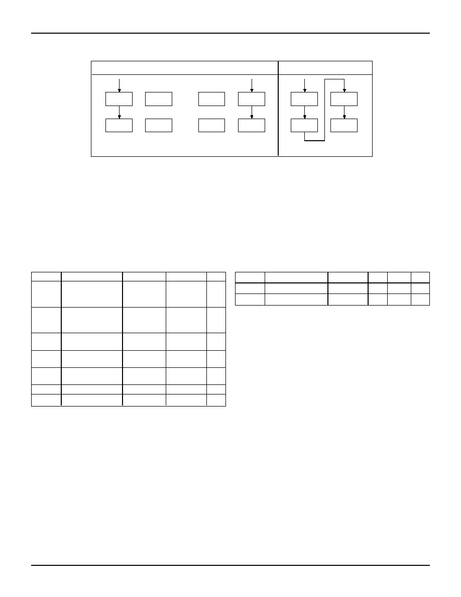
DESCRIPTION:
The IDT29FCT520A/B/C contains four 8-bit positive edge-
triggered registers. These may be operated as a dual 2-level
or as a single 4-level pipeline. A single 8-bit input is provided
and any of the four registers is available at the 8-bit, 3-state
output.
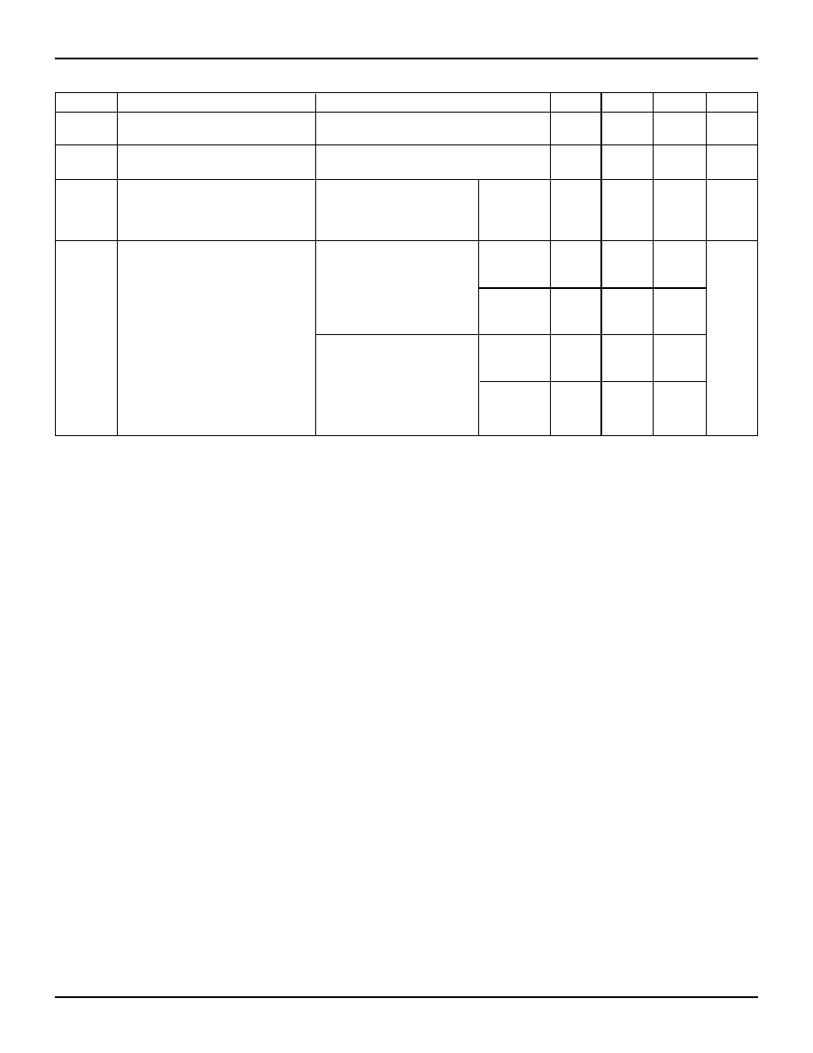
In the IDT29FCT520A/B/C when data is entered into the
first level (I = 2 or I = 1), the existing data in the first level is
moved to the second level. Transfer of data to the second
level is achieved using the 4-level shift instruction (I = 0). This
transfer also causes the first level to change.
FUNCTIONAL BLOCK DIAGRAMS
2620 drw 01
REGISTER
CONTROL
2
1
I ,I
1
0
CLK
OCTAL REG. A1
OCTAL REG. A2
OCTAL REG. B1
OCTAL REG. B2
MUX
MUX
2
S ,S
1
0
8
Y -Y
7
0
OE
8
D -D
7
0
The IDT logo is a registered trademark of Integrated Device Technology, Inc.
Æ
IDT29FCT520A
IDT29FCT520B
IDT29FCT520C
MULTILEVEL
PIPELINE REGISTER
1

7.2
2
IDT29FCT520A/B/C
MULTILEVEL PIPELINE REGISTER
MILITARY AND COMMERCIAL TEMPERATURE RANGES
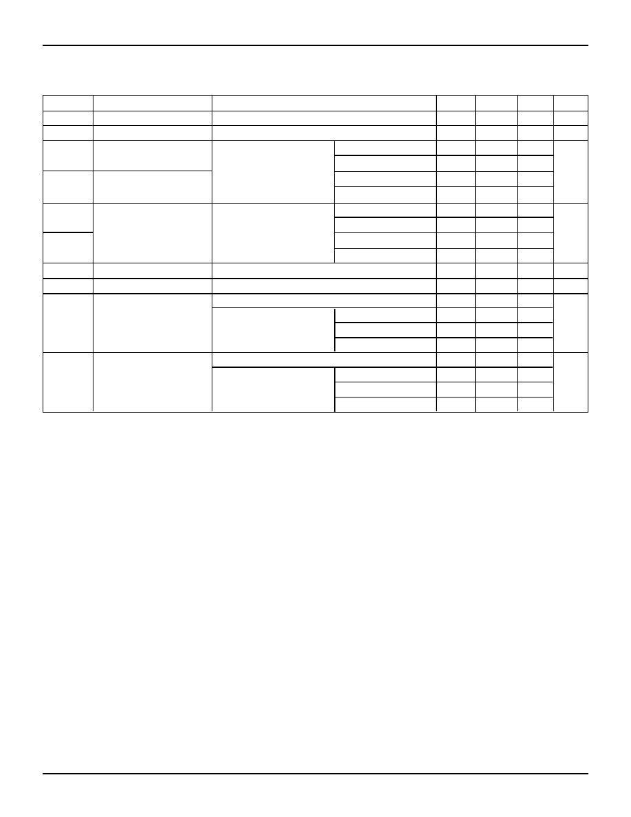
PIN CONFIGURATIONS
I
2620 drw 02
5
6
7
8
9
10
11
L28-1
25
24
23
22
21
20
19
INDEX
D
1
D
2
D
3
D
4
D
5
D
6
NC
Vcc
S
0
S
1
D
0
I
1
0
GND
NC
NC
NC
Y
0
Y
1
Y
2
Y
3
Y
4
Y
5
D
7
CLK
OE
Y
6
Y
7
12 13 14 15 16 17 18
4
3
2
1
28 27 26
DIP/CERPACK/SOIC
TOP VIEW
5
6
7
8
9
10
11
12
GND
1
2
3
4
24
23
22
21
20
19
18
17
Vcc
16
15
14
13
P24-1,
D24-1,
E24-1
&
SO24-2
S
0
S
1
Y
0
Y
1
Y
2
Y
3
Y
4
Y
5
OE
I
0
I
1
D
0
D
1
D
2
D
3
D
4
D
5
D
6
D
7
CLK
Y
6
Y
7
LCC
TOP VIEW
DEFINITION OF FUNCTIONAL TERMS
Pin Names
Description
D
n
Register input port.
CLK
Clock input. Enter data into registers on LOW-
to-HIGH transitions.
I
0
, I
1
Instruction inputs. See Figure 1 and In-
struction Control Tables.
S
0
, S
1
Multiplexer select. Inputs either register A
1
, A
2
,
B
1
or B
2
data to be available at the output port.
OE
Output enable for 3-state output port
Y
n
Register output port.
2620 tbl 01
REGISTER SELECTION
S
1
S
0
Register
0
0
B
2
0
1
B
1
1
0
A
2
1
1
A
1
2620 tbl 02
7.2
3
IDT29FCT520A/B/C
MULTILEVEL PIPELINE REGISTER
MILITARY AND COMMERCIAL TEMPERATURE RANGES
A
1
A
2
B
1
B
2
A
1
A
2
B
1
B
2
I = 2
I = 1
A
1
A
2
B
1
B
2
I = 0
DUAL 2-LEVEL
SINGLE 4-LEVEL
Figure 1. Data Loading in 2-Level Operation
NOTE:
1. I = 3 for hold.
2620 drw 03
CAPACITANCE
(T
A
= +25
∞
C, f = 1.0MHz)
Symbol Parameter
(1)
Conditions Typ.
Max.
Unit
C
IN
Input Capacitance
V
IN
= 0V
6
10
pF
C
OUT
Output Capacitance V
OUT
= 0V
8
12
pF
NOTE:
2620 tbl 04
1. This parameter is measured at characterization data but not tested.
ABSOLUTE MAXIMUM RATINGS
(1)
Symbol
Rating
Commercial
Military
Unit
V
TERM
(2)
Terminal Voltage
≠0.5 to +7.0 ≠0.5 to +7.0
V
with Respect
to GND
V
TERM
(3)
Terminal Voltage
≠0.5 to V
CC
≠0.5 to V
CC
V
with Respect
to GND
T
A
Operating
0 to +70
≠55 to +125
∞
C
Temperature
T
BIAS
Temperature
≠55 to +125 ≠65 to +135
∞
C
Under Bias
T
STG
Storage
≠55 to +125 ≠65 to +150
∞
C
Temperature
P
T
Power Dissipation
0.5
0.5
W
I
OUT
DC Output Current
120
120
mA
NOTES:
2620 tbl 03
1. Stresses greater than those listed under ABSOLUTE MAXIMUM
RATINGS may cause permanent damage to the device. This is a stress
rating only and functional operation of the device at these or any other
conditions above those indicated in the operational sections of this
specification is not implied. Exposure to absolute maximum rating
conditions for extended periods may affect reliability. No terminal voltage
may exceed V
CC
by +0.5V unless otherwise noted.
2. Inputs and V
CC
terminals.
3. Outputs and I/O terminals.
7.2
4
IDT29FCT520A/B/C
MULTILEVEL PIPELINE REGISTER
MILITARY AND COMMERCIAL TEMPERATURE RANGES
DC ELECTRICAL CHARACTERISTICS OVER OPERATING RANGE
Following Conditions Apply Unless Otherwise Specified: V
LC
= 0.2V, V
HC
= V
CC
≠ 0.2V
Commercial: T
A
= 0
∞
C to +70
∞
C, V
CC
= 5.0V
±
5%; Military: T
A
= ≠55
∞
C to +125
∞
C, V
CC
= 5.0V
±
10%
Symbol
Parameter
Test Conditions
(1)
Min.
Typ.
(2)
Max.
Unit
V
IH
Input HIGH Level
Guaranteed Logic HIGH Level
2.0
--
--
V
V
IL
Input LOW Level
Guaranteed Logic LOW Level
--
--
0.8
V
I
IH
Input HIGH Current
V
CC
= Max.
V
I
= V
CC
--
--
5
µ
A
V
I
= 2.7V
--
--
5
(4)
I
IL
Input LOW Current
V
I
=
0.5V
--
--
≠5
(4)
V
I
= GND
--
--
≠5
I
OZH
Off State (High Impedance) V
CC
= Max.
V
O
= V
CC
--
--
10
µ
A
Output Current
V
O
= 2.7V
--
--
10
(4)
I
OZL
V
O
=
0.5V
--
--
≠10
(4)
V
O
= GND
--
--
≠10
V
IK
Clamp Diode Voltage
V
CC
= Min., I
N
= ≠18mA
--
≠0.7
≠1.2
V
I
OS
Short Circuit Current
V
CC
= Max.
(3)
, V
O
= GND
≠60
≠120
--
mA
V
OH
Output HIGH Voltage
V
CC
= 3V, V
IN
= V
LC
or V
HC
, I
OH
= ≠32
µ
A
V
HC
V
CC
--
V
V
CC
= Min.
I
OH
= ≠300
µ
A
V
HC
V
CC
--
V
IN
= V
IH
or V
IL
I
OH
= ≠12mA MIL.
2.4
4.3
--
I
OH
= ≠15mA COM'L.
2.4
4.3
--
V
OL
Output LOW Voltage
V
CC
= 3V, V
IN
= V
LC
or V
HC
, I
OL
= 300
µ
A
--
GND
V
LC
V
V
CC
= Min.
I
OL
= 300
µ
A
--
GND
V
LC
(4)
V
IN
= V
IH
or V
IL
I
OL
= 32mA MIL.
--
0.3
0.5
I
OL
= 48mA COM'L.
--
0.3
0.5
NOTES:
2620 tbl 05
1. For conditions shown as Max. or Min., use appropriate value specified under Electrical Characteristics for the applicable device type.
2. Typical values are at V
CC
= 5.0V, +25
∞
C ambient and maximum loading.
3. Not more than one output should be shorted at one time. Duration of the short circuit test should not exceed one second.
4. This parameter is guaranteed but not tested.
7.2
5
IDT29FCT520A/B/C
MULTILEVEL PIPELINE REGISTER
MILITARY AND COMMERCIAL TEMPERATURE RANGES
POWER SUPPLY CHARACTERISTICS
V
LC
= 0.2V, V
HC
= V
CC
≠ 0.2V
Symbol
Parameter
Test Conditions
(1)
Min.
Typ.
(2)
Max.
Unit
I
CC
Quiescent Power
V
CC
= Max.
--
0.2
1.5
mA
Supply Current
V
IN
V
HC
; V
IN
V
LC
I
CC
Quiescent Power Supply
V
CC
= Max.
--
0.5
2.0
mA
Current, TTL Input HIGH
V
IN
= 3.4V
(3)
I
CCD
Dynamic Power Supply Current
(4)
V
CC
= Max., Outputs Open
V
IN
V
HC
--
0.15
0.25
mA/
OE
= GND
V
IN
V
LC
MHz
One Input Toggling
50% Duty Cycle
I
C
Total Power Supply Current
(6)
V
CC
= Max., Outputs Open
V
IN
V
HC
--
1.7
4.0
mA
f
CP
= 10MHz
V
IN
V
LC
50% Duty Cycle
(FCT)
OE
= GND
V
IN
= 3.4V
--
2.2
6.0
One Bit Toggling
V
IN
= GND
at f
i
= 5MHz, 50% Duty Cycle
V
CC
= Max., Outputs Open
V
IN
V
HC
--
7.0
12.8
(5)
f
CP
= 10MHz
V
IN
V
LC
50% Duty Cycle
(FCT)
OE
= GND
V
IN
= 3.4V
--
9.2
21.8
(5)
Eight Bits Toggling
V
IN
= GND
at f
i
= 5MHz, 50% Duty Cycle
NOTES:
2620 tbl 06
1. For conditions shown as Max. or Min., use appropriate value specified under Electrical Characteristics for the applicable device type.
2. Typical values are at V
CC
= 5.0V, +25
∞
C ambient.
3. Per TTL driven input (V
IN
= 3.4V); all other inputs at V
CC
or GND.
4. This parameter is not directly testable, but is derived for use in Total Power Supply calculations.
5. Values for these conditions are examples of the I
CC
formula. These limits are guaranteed but not tested.
6. I
C
= I
QUIESCENT
+I
INPUTS
+ I
DYNAMIC
I
C
= I
CC
+
I
CC
D
H
N
T
+ I
CCD
(f
CP
/2 + f
i
N
i
)
I
CC
= Quiescent Current
I
CC
= Power Supply Current for a TTL HIgh Input (V
IN
= 3.4V)
D
H
= Duty Cycle for TTL Inputs High
N
T
= Number of TTL inputs at D
H
I
CCD
= Dynamic Current Caused by an Input Transition Pair (HLH or LHL)
f
CP
= Clock Frequency for Register Devices (Zero for Non-Register Devices)
f
i
= Input Frequency
N
i
= Number of Inputs at f
i
All currents are in milliamps and all frequencies are in megahertz.