FCT_52t
1
IDT29FCT52AT/BT/CT/DT
FAST CMOS OCTAL REGISTERED TRANSCEIVER
INDUSTRIAL TEMPERATURE RANGE
JULY 2000
1999 Integrated Device Technology, Inc.
DSC-5483/-
c
IDT29FCT52AT/BT/CT/DT
INDUSTRIAL TEMPERATURE RANGE
FAST CMOS
OCTAL REGISTERED
TRANSCEIVER
DESCRIPTION:
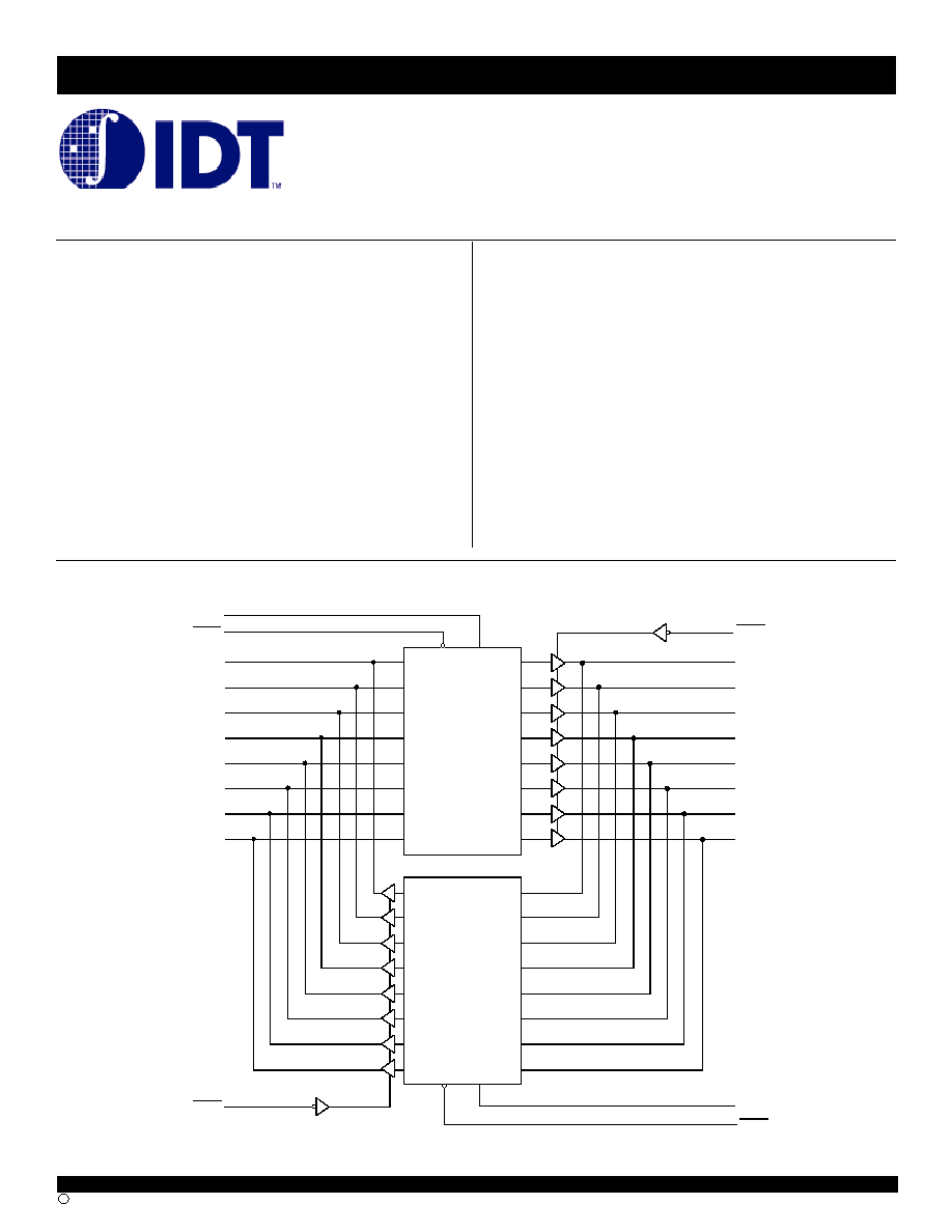
The IDT29FCT52T is an 8-bit registered transceiver built using an
advanced dual metal CMOS technology. Two 8-bit back-to-back registers
store data flowing in both directions between two bidirectional buses.
Separate clock, clock enable and 3-state output enable signals are provided
for each register. Both A outputs and B outputs are guaranteed to sink 64mA.
FUNCTIONAL BLOCK DIAGRAM
A
1
A
2
A
4
A
5
A
6
A
7
A
3
A
0
B
1
B
2
B
3
B
4
B
5
B
6
B
7
B
0
D
1
D
2
D
4
D
5
D
6
D
7
D
3
D
0
CE
CP
A
Reg.
Q
1
Q
2
Q
4
Q
5
Q
6
Q
7
Q
3
Q
0
D
1
D
2
D
4
D
5
D
6
D
7
D
3
D
0
CE
CP
B
Reg.
Q
1
Q
2
Q
4
Q
5
Q
6
Q
7
Q
3
Q
0
OEA
CPB
CEB
OEB
CPA
CEA
FEATURES:
-
Low input and output leakage
1� A (max.)
-
CMOS power levels
-
True TTL input and output compatibility
�
V
OH
= 3.3V (typ.)
�
V
OL
= 0.3V (typ.)
-
Meets or exceeds JEDEC standard 18 specifications
-
Available in SOIC, SSOP, and QSOP packages
-
A, B, C and D speed grades
-
High drive outputs (-15mA I
OH
, 64mA I
OL
)
-
Power off disable outputs permit "live insertion"
2
INDUSTRIAL TEMPERATURE RANGE
IDT29FCT52AT/BT/CT/DT
FAST CMOS OCTAL REGISTERED TRANSCEIVER
PIN CONFIGURATION
SOIC/ SSOP/ QSOP
TOP VIEW
2
3
1
20
19
18
15
16
9
10
A
6
A
7
A
1
A
0
A
2
A
5
A
3
A
4
B
6
B
7
23
22
24
21
17
5
6
7
4
SO24-2
SO24-7
SO24-8
8
V
CC
B
2
B
0
B
1
B
3
B
4
B
5
13
14
11
12
C EA
GND
OEB
C PA
OEA
C PB
C EB
OUTPUT CONTROL
(1)
Internal
OE
Q
Y-Outputs
Function
H
X
Z
Disable Outputs
L
L
L
Enable Outputs
L
H
H
NOTE:
1. H = HIGH Voltage Level
L = LOW Voltage Level
X = Don't Care
Z = High-Impedance
CAPACITANCE (T
A
= +25
O
C, f = 1.0MHz)
Symbol
Parameter
(1)
Conditions
Typ.
Max.
Unit
C
IN
Input Capacitance
V
IN
= 0V
6
10
pF
C
OUT
Output Capacitance
V
OUT
= 0V
8
12
pF
8T-link
NOTE:
1. This parameter is measured at characterization but not tested.
ABSOLUTE MAXIMUM RATINGS
(1)
Symbol
Rating
Max.
Unit
V
TERM(2)
Terminal Voltage with Respect to GND
�0.5 to +7
V
T
STG
Storage Temperature
�65 to +150
�C
I
OUT
DC Output Current
�65 to +120
mA
NOTES:
1. Stresses greater than those listed under ABSOLUTE MAXIMUM
RATINGS may cause permanent damage to the device. This is a
stress rating only and functional operation of the device at these or
any other conditions above those indicated in the operational sections
of this specification is not implied. Exposure to absolute maximum
rating conditions for extended periods may affect reliability.
2. All device terminals.
NOTE:
1. H = HIGH Voltage Level
L = LOW Voltage Level
X = Don't Care
NC = No Change
= LOW-to-HIGH Transition
REGISTER FUNCTION TABLE
(1)
(Applies to A or B Register)
Inputs
Internal
D
CP
CE
Q
Function
X
X
H
N C
Hold Data
L
L
L
Load Data
H
L
H
3
IDT29FCT52AT/BT/CT/DT
FAST CMOS OCTAL REGISTERED TRANSCEIVER
INDUSTRIAL TEMPERATURE RANGE
PIN DESCRIPTION
Name
I/O
Description
A
0-7
I/O
Eight bidirectional lines carrying the A Register inputs or B Register outputs.
B
0-7
I/O
Eight bidirectional lines carrying the B Register inputs or A Register outputs.
CPA
I
Clock for the A Register. When
CEA is LOW, data is entered into the A Register on the LOW-to-HIGH transition of the CPA signal.
CEA
I
Clock Enable for the A Register. When
CEA is LOW, data is entered into the A Register on the LOW-to-HIGH transition of the CPA signal. When
CEA is HIGH, the A Register holds its contents, regardless of CPA signal transitions.
OEB
I
Output Enable for the A Register. When
OEB is LOW, the A Register outputs are enabled onto the B
0-7
lines. When
OEB is HIGH, the B
0-7
outputs
are in the high-impedance state.
CPB
I
Clock for the B Register. When
CEB is LOW, data is entered into the B Register on the LOW-to-HIGH transition of the CPB signal.
CEB
I
Clock Enable for the B Register. When
CEB is LOW, data is entered into the B Register on the LOW-to-HIGH transition of the CPB signal. When
CEB is HIGH, the B Register holds its contents, regardless of CPB signal transitions.
OEA
I
Output Enable for the B Register. When
OEA is LOW, the B Register outputs are enabled onto the A
0-7
lines. When
OEA is HIGH, the A
0-7
outputs
are in the high-impedance state.
NOTES:
1. For conditions shown as Max. or Min., use appropriate value specified under Electrical Characteristics for the applicable device type.
2. Typical values are at V
CC
= 5.0V, +25�C ambient.
3. Not more than one output should be shorted at one time. Duration of the short circuit test should not exceed one second.
4. The test limit for this parameter is �5
�
A at T
A
= -55�C.
5. This parameter is guaranteed but not tested.
DC ELECTRICAL CHARACTERISTICS OVER OPERATING RANGE
Following Conditions Apply Unless Otherwise Specified:
Industrial: T
A
= -40�C to +85�C, V
CC
= 5.0V � 5%
Symbol
Parameter
Test Conditions
(1)
Min.
Typ.
(2)
Max.
Unit
V
IH
Input HIGH Level
Guaranteed Logic HIGH Level
2
--
--
V
V
IL
Input LOW Level
Guaranteed Logic LOW Level
--
--
0.8
V
I
IH
Input HIGH Current
(4)
V
CC
= Max.
V
I
= 2.7V
--
--
�1
� A
I
IL
Input LOW Current
(4)
V
I
= 0.5V
--
--
�1
I
OZH
High Impedance Output Current
V
CC
= Max.
V
O
= 2.7V
--
--
�1
I
OZL
(3-State Output pins)
(4)
V
O
= 0.5V
--
--
�1
I
I
Input HIGH Current
(4)
V
CC
= Max., V
I
= V
CC
(Max.)
--
--
�1
� A
V
IK
Clamp Diode Voltage
V
CC
= Min., I
IN
= �18mA
--
�0.7
�1.2
V
V
H
Input Hysteresis
--
--
200
--
mV
I
CC
Quiescent Power Supply Current
V
CC
= 3V, V
IN
= GND or V
CC
--
0.01
1
mA
OUTPUT DRIVE CHARACTERISTICS
Symbol
Parameter
Test Conditions
(1)
Min.
Typ.
(2)
Max.
Unit
V
OH
Output HIGH Voltage
V
CC
= Min.
I
OH
= -8mA
2.4
3.3
--
V
V
IN
= V
IH
or
V
IL
I
OH
= -15mA
2
3
--
V
OL
Output LOW Voltage
V
CC
= Min.
I
OL
= 64mA
--
0.3
0.55
V
V
IN
= V
IH
or
V
IL
I
OS
Short Circuit Current
V
CC
= Max., V
O
= GND
(3)
�60
�120
�225
mA
I
OFF
Input/Output Power Off Leakage
(5)
V
CC
= 0V, V
IN
or V
O
4.5V
--
--
�1
� A
4
INDUSTRIAL TEMPERATURE RANGE
IDT29FCT52AT/BT/CT/DT
FAST CMOS OCTAL REGISTERED TRANSCEIVER
NOTES:
1. For conditions shown as Max. or Min., use appropriate value specified under Electrical Characteristics for the applicable device type.
2. Typical values are at V
CC
= 5.0V, +25�C ambient.
3. Per TTL driven input (V
IN
= 3.4V). All other inputs at V
CC
or GND.
4. This parameter is not directly testable, but is derived for use in Total Power Supply Calculations.
5. Values for these conditions are examples of the I
CC
formula. These limits are guaranteed but not tested.
6. I
C
= I
QUIESCENT
+ I
INPUTS
+ I
DYNAMIC
I
C
= I
CC
+
I
CC
D
H
N
T
+ I
CCD
(f
CP/
2 + f
i
N
i
)
I
CC
= Quiescent Current
I
CC
= Power Supply Current for a TTL High Input (V
IN
= 3.4V)
D
H
= Duty Cycle for TTL Inputs High
N
T
= Number of TTL Inputs at D
H
I
CCD
= Dynamic Current Caused by an Input Transition Pair (HLH or LHL)
f
CP
= Clock Frequency for Register Devices (Zero for Non-Register Devices)
f
i
= Input Frequency
N
i
= Number of Inputs at f
i
All currents are in milliamps and all frequencies are in megahertz.
POWER SUPPLY CHARACTERISTICS
Symbol
Parameter
Test Conditions
(1)
Min.
Typ.
(2)
Max.
Unit
I
CC
Quiescent Power Supply Current
TTL Inputs HIGH
V
CC
= Max.
V
IN
= 3.4V
(3)
--
0.5
2
mA
I
CCD
Dynamic Power Supply Current
(4)
V
CC
= Max.
Outputs Open
OE
A
or
OE
B
= GND
V
IN
= V
CC
V
IN
= GND
--
0.15
0.25
mA/
MHz
One Input Toggling
50% Duty Cycle
I
C
Total Power Supply Current
(6)
V
CC
= Max.
Outputs Open
V
IN
= V
CC
V
IN
= GND
--
1.5
3.5
mA
f
CP
= 10MHz
50% Duty Cycle
OE
A
or
OE
B
= GND
V
IN
= 3.4V
--
2
5.5
One Bit Toggling
at fi = 5MHz
50% Duty Cycle
V
IN
= GND
V
CC
= Max.
Outputs Open
V
IN
= V
CC
V
IN
= GND
--
3.8
7.3
(5)
f
CP
= 10MHz
50% Duty Cycle
OE
A
or
OE
B
= GND
V
IN
= 3.4V
--
6
16.3
(5)
Eight Bits Toggling
at fi = 2.5MHz
50% Duty Cycle
V
IN
= GND
5
IDT29FCT52AT/BT/CT/DT
FAST CMOS OCTAL REGISTERED TRANSCEIVER
INDUSTRIAL TEMPERATURE RANGE
NOTES:
1. See test circuit and waveforms.
2. Minimum limits are guaranteed but not tested on Propagation Delays.
3. This parameter is guaranteed but not tested.
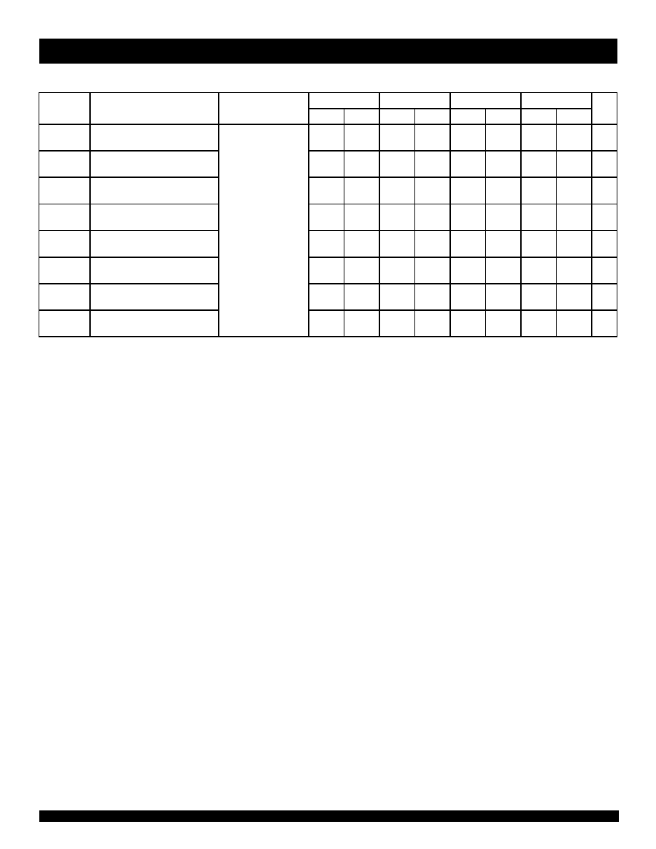
SWITCHING CHARACTERISTICS OVER OPERATING RANGE
(1)
29FCT52AT
29FCT52BT
29FCT52CT
29FCT52DT
Symbol
Parameter
Condition
(1)
Min
.
(2)
Max.
Min
.
(2)
Max.
Min
.
(2)
Max.
Min
.
(2)
Max.
Unit
t
PLH
t
PHL
Propagation Delay
CPA, CPB to An, Bn
C
L
= 50pF
R
L
= 500
2
10
2
7.5
2
6.3
2
4.5
ns
t
PZH
t
PZL
Output Enable Time
OEA or OEB to An, Bn
1.5
10.5
1.5
8
1.5
7
1.5
5.6
ns
t
PHZ
t
PLZ
Output Disable Time
OEA or OEB to An, Bn
1.5
10
1.5
7.5
1.5
6.5
1.5
4.3
ns
t
SU
Set-up Time, HIGH or LOW
An, Bn to CPA, CPB
2.5
--
2.5
--
2.5
--
1.5
--
ns
t
H
Hold Time, HIGH or LOW
An, Bn to CPA, CPB
2
--
1.5
--
1.5
--
1
--
ns
t
SU
Set-up Time, HIGH or LOW
CEA, CEB to CPA, CPB
3
--
3
--
3
--
2
--
ns
t
H
Hold Time, HIGH or LOW
CEA, CEB to CPA, CPB
2
--
2
--
2
--
1
--
ns
t
W
Clock Pulse Width HIGH or
LOW
(3)
3
--
3
--
3
--
3
--
ns