Integrated Device Technology, Inc.
MILITARY AND COMMERCIAL TEMPERATURE RANGES
MAY 1992
©
1992 Integrated Device Technology, Inc.
7.1
DSC-4605/3
Æ
FAST CMOS
OCTAL REGISTERED
TRANSCEIVERS
FEATURES:
∑ Equivalent to AMD's Am2952/53 and National's
29F52/53 in pinout/function
∑ IDT29FCT52A/53A equivalent to FAST
TM
speed
∑ IDT29FCT52B/53B 25% faster than FAST
∑ IDT29FCT52C/53C 37% faster than FAST
∑ I
OL
= 64mA (commercial) and 48mA (military)
∑ I
IH
and I
IL
only 5
µ
A max.
∑ CMOS power levels (2.5mW typ. static)
∑ TTL input and output level compatible
∑ CMOS output level compatible
∑ Available in 24-pin DIP, SOIC, 28-pin LCC with JEDEC
standard pinout
∑ Product available in Radiation Tolerant and Radiation
Enhanced versions
∑ Military product compliant to MIL-STD-883, Class B
DESCRIPTION:
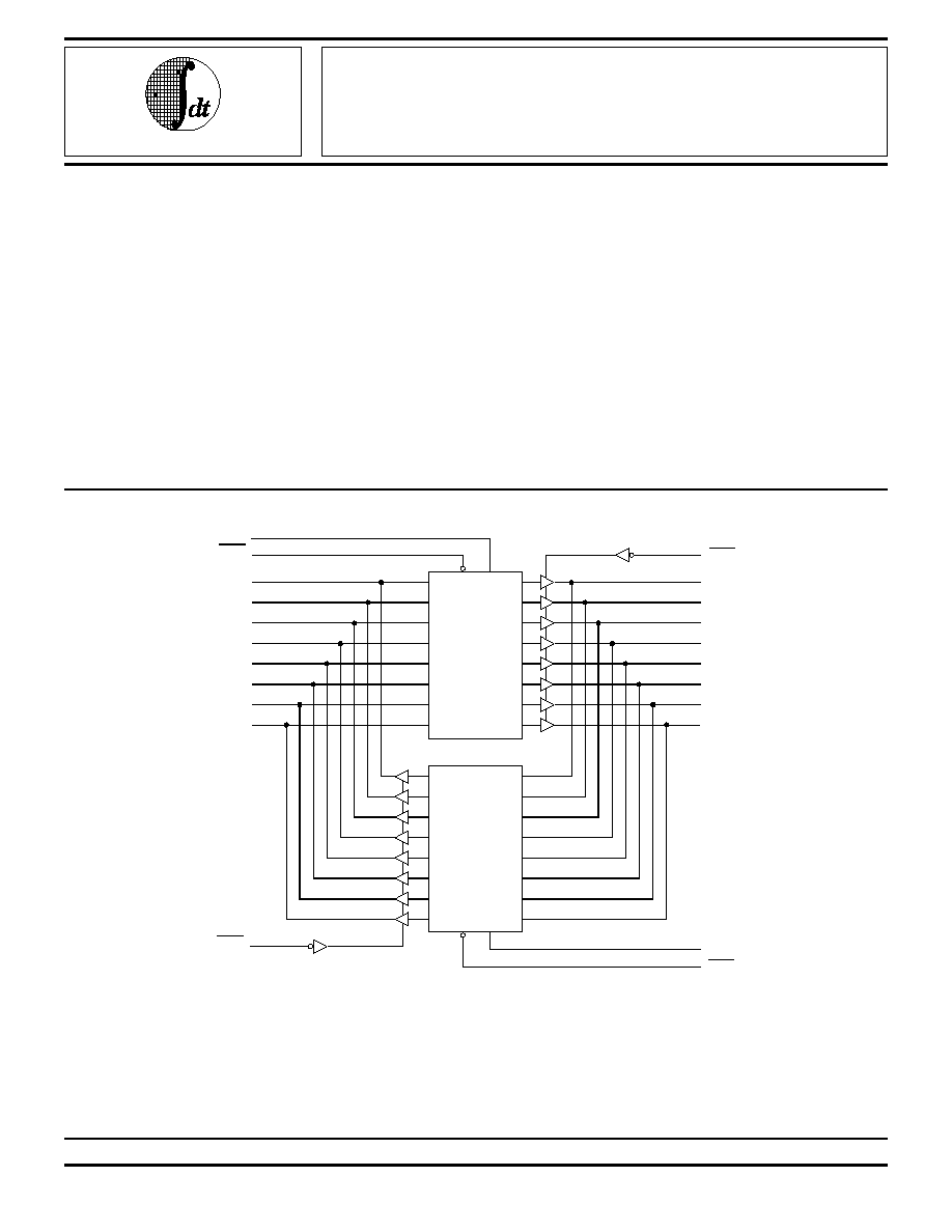
The IDT29FCT52A/B/C and IDT29FCT53A/B/C are 8-bit
registered transceivers manufactured using an advanced
dual metal CMOS technology. Two 8-bit back-to-back regis-
ters store data flowing in both directions between two bidirec-
tional buses. Separate clock, clock enable and 3-state output
enable signals are provided for each register. Both A outputs
and B outputs are guaranteed to sink 64mA.
The IDT29FCT52A/B/C is a non-inverting option of the
IDT29FCT53A/B/C.
CPA
A
0
CEA
A
1
A
2
A
3
A
4
A
5
A
6
A
7
B
0
OEB
B
1
B
2
B
3
B
4
B
5
B
6
B
7
Q
0
Q
1
Q
2
Q
3
Q
4
Q
5
Q
6
Q
7
D
0
D
1
D
2
D
3
D
4
D
5
D
6
D
7
CE CP
A
Reg.
D
0
D
1
D
2
D
3
D
4
D
5
D
6
D
7
Q
0
Q
1
Q
2
Q
3
Q
4
Q
5
Q
6
Q
7
CE CP
B
Reg.
OEA
CPB
CEB
The IDT logo is a registered trademark of Integrated Device Technology, Inc.
FAST is a trademark of National Semiconductor Co.
IDT29FCT52A/B/C
IDT29FCT53A/B/C
FUNCTIONAL BLOCK DIAGRAM
(1)
NOTE:
2533 drw 01
1. IDT29FCT52 function is shown.
1
7.1
2
IDT29FCT52A/B/C, IDT29FCT53A/B/C
FAST CMOS OCTAL REGISTERED TRANSCEIVERS
MILITARY AND COMMERCIAL TEMPERATURE RANGES
PIN DESCRIPTION
Name
I/O
Description
A
0-7
I/O
Eight bidirectional lines carrying the A Register inputs or B Register outputs.
B
0-7
I/O
Eight bidirectional lines carrying the B Register inputs or A Register outputs.
CPA
I
Clock for the A Register. When
CEA
is LOW, data is entered into the A Register on the LOW-to-HIGH transition
of the CPA signal.
CEA
I
Clock Enable for the A Register. When
CEA
is LOW, data is entered into the A Register on the LOW-to-HIGH
transition of the CPA signal. When
CEA
is HIGH, the A Register holds its contents, regardless of CPA signal
transitions.
OEB
I
Output Enable for the A Register. When
OEB
is LOW, the A Register outputs are enabled onto the B
0-7
lines. When
OEB
is HIGH, the B
0-7
outputs are in the high-impedance state.
CPB
I
Clock for the B Register. When
CEB
is LOW, data is entered into the B Register on the LOW-to-HIGH transition
of the CPB signal.
CEB
I
Clock Enable for the B Register. When
CEB
is LOW, data is entered into the B Register on the LOW-to-HIGH
transition of the CPB signal. When
CEB
is HIGH, the B Register holds its contents, regardless of CPB signal
transitions.
OEA
I
Output Enable for the B Register. When
OEA
is LOW, the B Register outputs are enabled onto the A
0-7
lines. When
OEA
is HIGH, the A
0-7
outputs are in the high-impedance state.
2533 tbl 01
PIN CONFIGURATIONS
DIP/CERPACK/SOIC
TOP VIEW
5
6
7
8
9
10
11
12
GND
1
2
3
4
24
23
22
21
20
19
18
17
Vcc
16
15
14
13
P24-1,
D24-1,
E24-1
&
SO24-2
A
6
A
5
A
4
A
3
A
2
CEB
CEA
CPB
CPA
OEA
A
1
A
0
A
7
B
6
B
5
B
4
B
3
B
2
B
1
B
B
7
0
OEB
REGISTER FUNCTION TABLE
(1)
(Applies to A or B Register)
Inputs
Internal
D
CP
CE
CE
Q
Function
X
X
H
NC
Hold Data
L
L
L
Load Data
H
L
H
2533 tbl 02
OUTPUT CONTROL
(1)
Internal
Y-Outputs
OE
OE
Q
52
53
Function
H
X
Z
Z
Disable Outputs
L
L
L
H
Enable Outputs
L
H
H
L
NOTE:
2533 tbl 03
1. H = HIGH Voltage Level
L = LOW Voltage Level
X = Don't Care
NC = No Change
= LOW-to-HIGH Transition
5
6
7
8
9
10
11
L28-1
25
24
23
22
21
20
19
INDEX
B
4
B
3
B
2
B
1
B
0
OEB
NC
Vcc
A
7
A
6
B
5
B
6
B
7
GND
CPA
CEA
NC
CEB
CPB
OEA
NC
NC
A
5
A
4
A
3
A
2
A
1
A
0
12 13 14 15 16 17 18
4
3
2
1
28 27 26
LCC
TOP VIEW
2533 drw 02

7.1
3
IDT29FCT52A/B/C, IDT29FCT53A/B/C
FAST CMOS OCTAL REGISTERED TRANSCEIVERS
MILITARY AND COMMERCIAL TEMPERATURE RANGES
DC ELECTRICAL CHARACTERISTICS OVER OPERATING RANGE
Following Conditions Apply Unless Otherwise Specified: V
LC
= 0.2V; V
HC
= V
CC
≠ 0.2V
Commercial: T
A
= 0
∞
C to +70
∞
C, V
CC
= 5.0V
±
5%; Military: T
A
= ≠55
∞
C to +125
∞
C, V
CC
= 5.0V
±
10%
Symbol
Parameter
Test Conditions
(1)
Min.
Typ.
(2)
Max.
Unit
V
IH
Input HIGH Level
Guaranteed Logic HIGH Level
2.0
--
--
V
V
IL
Input LOW Level
Guaranteed Logic LOW Level
--
--
0.8
V
I
IH
Input HIGH Current
V
CC
= Max.
V
I
=V
CC
--
--
5
µ
A
(Except I/O Pins)
V
I
= 2.7V
--
--
5
(4)
I
IL
Input LOW Current
V
I
= 0.5V
--
--
≠5
(4)
(Except I/O Pins)
V
I
= GND
--
--
≠5
I
IH
Input HIGH Current
V
CC
= Max.
V
I
= V
CC
--
--
15
µ
A
(I/O Pins Only)
V
I
= 2.7V
--
--
15
(4)
I
IL
Input LOW Current
V
I
= 0.5V
--
--
≠15
(4)
(I/O Pins Only)
V
I
= GND
--
--
≠15
V
IK
Clamp Diode Voltage
Vcc = Min., I
N
= ≠18mA
--
≠0.7
≠1.2
V
I
OS
Short Circuit Current
Vcc = Max.
(3)
, V
O
= GND
≠60
≠120
--
mA
V
OH
Output HIGH Voltage
Vcc = 3V, V
IN
= V
LC
or V
HC
, I
OH
= ≠32
µ
A
V
HC
V
CC
--
V
Vcc = Min.
I
OH
= ≠300
µ
A
V
HC
V
CC
--
V
IN
= V
IH
or V
IL
I
OH
= ≠15mA MIL.
2.4
4.0
--
I
OH
= ≠24mA COM'L.
2.4
4.0
--
V
OL
Output LOW Voltage
Vcc = 3V, V
IN
= V
LC
or V
HC
, I
OL
= 300
µ
A
--
GND
V
LC
V
Vcc = Min.
I
OL
= 300
µ
A
--
GND
V
LC
(4)
V
IN
= V
IH
or V
IL
I
OL
= 48mA MIL.
(5)
--
0.3
0.55
I
OL
= 64mA COM'L.
(5)
--
0.3
0.55
NOTES:
2533 tbl 06
1. For conditions shown as Max. or Min., use appropriate value specified under Electrical Characteristics for the applicable device type.
2. Typical values are at V
CC
= 5.0V, +25
∞
C ambient and maximum loading.
3. Not more than one output should be shorted at one time. Duration of the short circuit test should not exceed one second.
4. This parameter is guaranteed but not tested.
5. These are maximum I
OL
values per output, for 8 outputs turned on simultaneously. Total maximum I
OL
(all outputs) is 512mA for commercial and
384mA for military. Derate I
OL
for number of outputs exceeding 8 turned on simultaneously.
ABSOLUTE MAXIMUM RATINGS
(1)
Symbol
Rating
Commercial
Military
Unit
V
TERM
(2)
Terminal Voltage
≠0.5 to +7.0
≠0.5 to +7.0
V
with Respect
to GND
V
TERM
(3)
Terminal Voltage
≠0.5 to V
CC
≠0.5 to V
CC
V
with Respect
to GND
T
A
Operating
0 to +70
≠55 to +125
∞
C
Temperature
T
BIAS
Temperature
≠55 to +125
≠65 to +135
∞
C
Under Bias
T
STG
Storage
≠55 to +125
≠65 to +150
∞
C
Temperature
P
T
Power Dissipation
0.5
0.5
W
I
OUT
DC Output Current
120
120
mA
NOTES:
2533 tbl 04
1. Stresses greater than those listed under ABSOLUTE MAXIMUM
RATINGS may cause permanent damage to the device. This is a stress
rating only and functional operation of the device at these or any other
conditions above those indicated in the operational sections of this
specification is not implied. Exposure to absolute maximum rating
conditions for extended periods may affect reliability. No terminal voltage
may exceed +0.5V unless otherwise noted.
2. Inputs and V
CC
terminals only.
3. Outputs and I/O terminals only.
CAPACITANCE
(T
A
= +25
∞
C, f = 1.0MHz)
Symbol
Parameter
(1)
Conditions
Typ.
Max.
Unit
C
IN
Input
V
IN
= 0V
6
10
pF
Capacitance
C
I/O
I/O
V
OUT
= 0V
8
12
pF
Capacitance
NOTE:
2533 tbl 05
1. This parameter is guaranteed by characterization data and not tested.

7.1
4
IDT29FCT52A/B/C, IDT29FCT53A/B/C
FAST CMOS OCTAL REGISTERED TRANSCEIVERS
MILITARY AND COMMERCIAL TEMPERATURE RANGES
POWER SUPPLY CHARACTERISTICS
V
LC
= 0.2V; V
HC
= V
CC
≠ 0.2V
Symbol
Parameter
Test Conditions
(1)
Min.
Typ.
(2)
Max.
Unit
I
CC
Quiescent Power Supply
V
CC
= Max.
--
0.5
1.5
µ
A
Current
V
IN
V
HC
; V
IN
V
LC
I
CC
Quiescent Power Supply
Vcc = Max.
--
0.5
2.0
mA
Current TTL Inputs HIGH
V
IN
= 3.4V
(3)
I
CCD
Dynamic Power Supply
Vcc = Max.
V
IN
V
HC
--
0.15
0.25
mA/
Current
(4)
Outputs Open
V
IN
V
LC
MHz
OEA
or
OEB
= GND
One Input Toggling
50% Duty Cycle
I
C
Total Power Supply
Vcc = Max.
V
IN
V
HC
--
2.0
4.0
mA
Current
(6)
Outputs Open
V
IN
V
LC
f
CP
= 10MHz
(FCT)
50% Duty Cycle
OEA
or
OEB
= GND
One Bit Toggling
V
IN
= 3.4V
--
2.5
6.0
at fi = 5MHz
V
IN
= GND
50% Duty Cycle
V
CC
= Max.
V
IN
V
HC
--
4.3
7.8
(5)
Outputs Open
V
IN
V
LC
f
CP
= 10MHz
(FCT)
50% Duty Cycle
OEA
or
OEB
= GND
Eight Bits Toggling
V
IN
= 3.4V
--
6.5
16.8
(5)
at f
i
= 2.5MHz
V
IN
= GND
50% Duty Cycle
NOTES:
2533 tbl 07
1. For conditions shown as Max. or Min., use appropriate value specified under Electrical Characteristics for the applicable device type.
2. Typical values are at V
CC
= 5.0V, +25
∞
C ambient.
3. Per TTL driven input (V
IN
= 3.4V); all other inputs at V
CC
or GND.
4. This parameter is not directly testable, but is derived for use in Total Power Supply calculations.
5. Values for these conditions are examples of the I
CC
formula. These limits are guaranteed but not tested.
6. I
C
= I
QUIESCENT
+ I
INPUTS
+ I
DYNAMIC
I
C
= I
CC
+
I
CC
D
H
N
T
+ I
CCD
(f
CP
/2 + f
i
N
i
)
I
CC
= Quiescent Current
I
CC
= Power Supply Current for a TTL High Input (V
IN
= 3.4V)
D
H
= Duty Cycle for TTL Inputs High
N
T
= Number of TTL Inputs at D
H
I
CCD
= Dynamic Current Caused by an Output Transition Pair (HLH or LHL)
f
CP
= Clock Frequency for Register Devices (Zero for Non-Register Devices)
f
i
= Input Frequency
N
i
= Number of Inputs at f
i
All currents are in milliamps and all frequencies are in megahertz.

7.1
5
IDT29FCT52A/B/C, IDT29FCT53A/B/C
FAST CMOS OCTAL REGISTERED TRANSCEIVERS
MILITARY AND COMMERCIAL TEMPERATURE RANGES
t
PLH
Propagation Delay
C
L
= 50pF
2.0
10.0
2.0
11.0
2.0
7.5
2.0
8.0
2.0
6.3
2.0
7.3
ns
t
PHL
CPA, CPB to A
n
, B
n
R
L
= 500
t
PZH
Output Enable Time
1.5
10.5
1.5
13.0
1.5
8.0
1.5
8.5
1.5
7.0
1.5
8.0
ns
t
PZL
OEA
or
OEB
to
A
n
or B
n
t
PHZ
Output Disable Time
1.5
10.0
1.5
10.0
1.5
7.5
1.5
8.0
1.5
6.5
1.5
7.5
ns
t
PLZ
OEA
or
OEB
to
A
n
or B
n
t
SU
Set-up Time HIGH
2.5
--
2.5
--
2.5
--
2.5
--
2.5
--
2.5
--
ns
or LOW A
n
, B
n
to
CPA, CPB
t
H
Hold Time HIGH
2.0
--
2.0
--
1.5
--
1.5
--
1.5
--
1.5
--
ns
or LOW A
n
, B
n
to
CPA, CPB
t
SU
Set-up Time HIGH
3.0
--
3.0
--
3.0
--
3.0
--
3.0
--
3.0
--
ns
or
LOW
CEA
,
CEB
to
CPA, CPB
t
H
Hold Time HIGH
2.0
--
2.0
--
2.0
--
2.0
--
2.0
--
2.0
--
ns
or LOW
CEA
,
CEB
to
CPA, CPB
t
W
Pulse Width, HIGH
(3)
3.0
--
3.0
--
3.0
--
3.0
--
3.0
--
3.0
--
ns
or LOW CPA or CPB
NOTES:
2533 tbl 08
1. See test circuit and waveforms.
2. Minimum limits are guaranteed but not tested on Propagation Delays.
3. This parameter is guaranteed but not tested.
SWITCHING CHARACTERISTICS OVER OPERATING RANGE
IDT29FCT52A/53A
IDT29FCT52B/53B
IDT29FCT52C/53C
Com'l.
Mil.
Com'l.
Mil.
Com'l.
Mil.
Symbol
Parameter
Condition
(1)
Min.
(2)
Max. Min.
(2)
Max. Min.
(2)
Max. Min.
(2)
Max.
Min.
(2)
Max. Min
.
(2)
Max.
Unit

7.1
6
IDT29FCT52A/B/C, IDT29FCT53A/B/C
FAST CMOS OCTAL REGISTERED TRANSCEIVERS
MILITARY AND COMMERCIAL TEMPERATURE RANGES
TEST CIRCUITS AND WAVEFORMS
TEST CIRCUITS FOR ALL OUTPUTS
ENABLE AND DISABLE TIMES
PROPAGATION DELAY
SET-UP, HOLD AND RELEASE TIMES
PULSE WIDTH
Pulse
Generator
DATA
INPUT
TIMING
INPUT
ASYNCHRONOUS CONTROL
PRESET
CLEAR
ETC.
SYNCHRONOUS CONTROL
PRESET
CLEAR
CLOCK ENABLE
ETC.
3V
1.5V
0V
3V
1.5V
0V
3V
1.5V
0V
3V
1.5V
0V
t
SU
t
H
t
REM
H
t
SU
R
T
D.U.T.
V
CC
V
IN
C
L
V
OUT
50pF
500
500
7.0V
SAME PHASE
INPUT TRANSITION
3V
1.5V
0V
1.5V
V
OH
V
OL
t
PLH
t
PHL
OUTPUT
OPPOSITE PHASE
INPUT TRANSITION
CONTROL
INPUT
3V
1.5V
0V
3.5V
0V
OUTPUT
NORMALLY
LOW
OUTPUT
NORMALLY
HIGH
SWITCH
CLOSED
SWITCH
OPEN
V
OL
V
OH
3V
1.5V
0V
t
PLH
t
PHL
0.3V
0.3V
t
PLZ
t
PZL
t
PZH
t
PHZ
3.5V
0V
1.5V
1.5V
ENABLE
DISABLE
HIGH-LOW-HIGH
PULSE
LOW-HIGH-LOW
PULSE
t
W
1.5V
1.5V
t
NOTES
2533 drw 04
1. Diagram shown for input Control Enable-LOW and input Control
Disable-HIGH.
2. Pulse Generator for All Pulses: Rate
1.0 MHz; Z
O
50
; t
F
2.5ns;
t
R
2.5ns.
SWITCH POSITION
Test
Switch
Open Drain
Disable Low
Closed
Enable Low
All Other Tests
Open
DEFINITIONS:
2533 tbl 09
C
L
= Load capacitance: includes jig and probe capacitance.
R
T
= Termination resistance: should be equal to Z
OUT
of the Pulse
Generator.
7.1
7
IDT29FCT52A/B/C, IDT29FCT53A/B/C
FAST CMOS OCTAL REGISTERED TRANSCEIVERS
MILITARY AND COMMERCIAL TEMPERATURE RANGES
ORDERING INFORMATION
XXX
Package
X
Process/
Temperature
Range
Blank
B
Commercial (0
∞
C to +70
∞
C)
Military (≠55
∞
C to +125
∞
C)
Compliant to MIL-STD-883, Class B
P
D
E
L
SO
Plastic DIP
CERDIP
CERPACK
Leadless Chip Carrier
Small Outline IC
52A
53A
52B
53B
52C
53C
Non-Inverting Octal Registered Transceiver
Inverting Octal Registered Transceiver
Fast Non-Inverting Octal Registered Transceiver
Fast Inverting Octal Registered Transceiver
Super Fast Non-Inverting Octal Registered Transceiver
Super Fast Inverting Octal Registered Transceiver
X
Device
Type
2533 drw 03
IDT29FCT