1
IDT49C466, IDT49C466A
64-BIT FLOW-THRU ERROR DETECTION AND CORRECTION UNIT
COMMERCIAL TEMPERATURE RANGE
FEBRUARY 2000
1999 Integrated Device Technology, Inc.
DSC-2617/9
c
IDT49C466
IDT49C466A
COMMERCIAL TEMPERATURE RANGE
64-BIT FLOW-THRU
ERROR DETECTION
AND CORRECTION UNIT
DESCRIPTION:
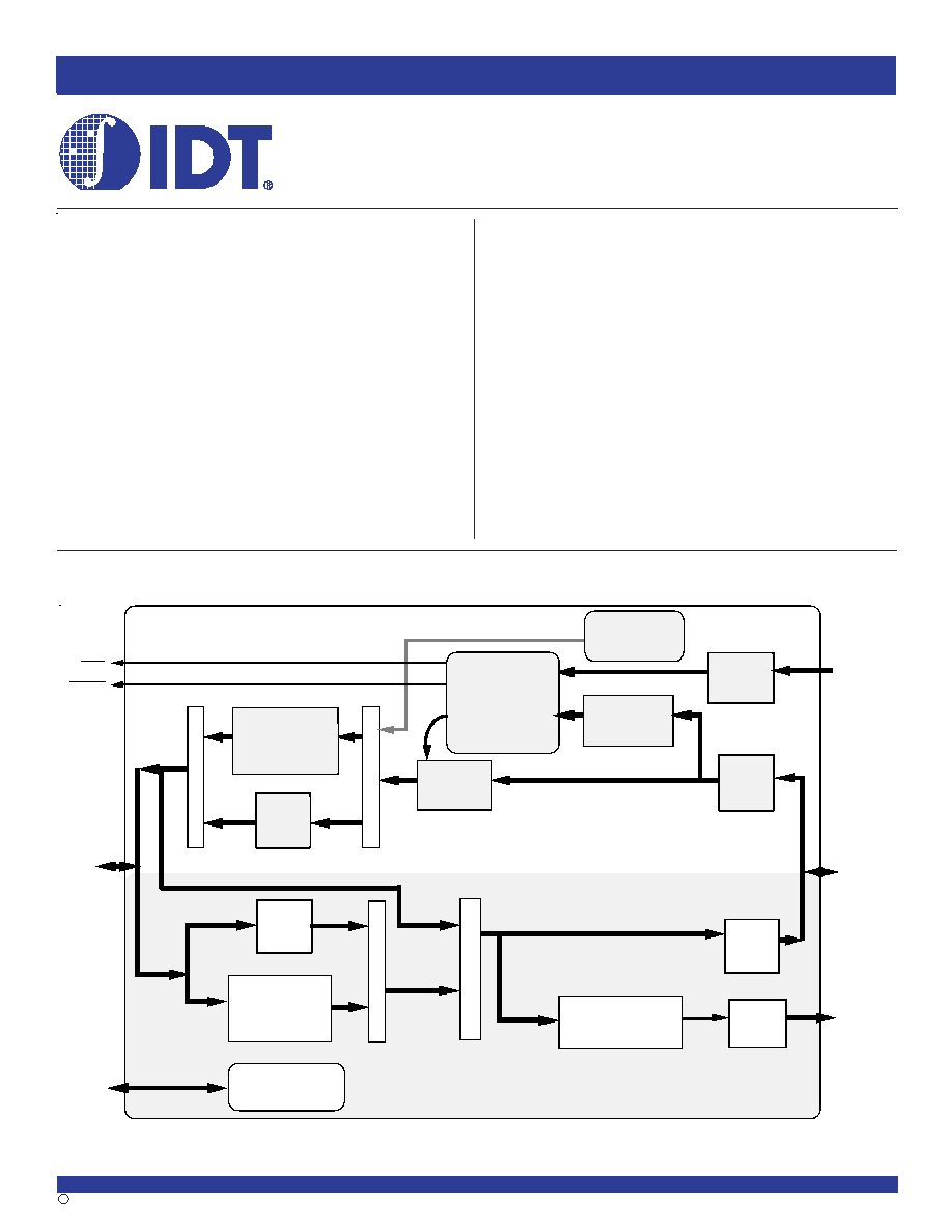
The IDT49C466/A 64-bit Flow-thruEDC is a high-speed error detection
and correction unit that ensures data integrity in memory systems. The flow-
thru architecture, with separate system and memory data buses, is ideally
suited for pipelined memory systems.
Implementing a modified Hamming code, the IDT49C466/A corrects all
single bit hard and soft errors, and detects all double bit errors. The read/
write FIFOs can store up to sixteen words. FIFO full and empty flags indicate
whether additional data can be written to or read from the EDC.
Check bit generation for partial word writes on byte boundaries is
supported on the IDT49C466/A.
Diagnostic features include a check bit register, syndrome registers, a
four bit error counter which logs up to fifteen errors, and an error data
register which stores the complete error data word. Parity can be generated
and checked on the system bus by the IDT49C466/A.
FUNCTIONAL BLOCK DIAGRAM
SD
CHK-BIT
LATCH
W RITE
BUFFER
16 W O RDS BY
72
SD
LATCH
IN
M D
LATCH
O UT
R EAD BU FFER
16 W O RDS BY
64
M D
LATCH
IN
SD
LATCH
O UT
ERRO R
CO RRECT
CHEC K-BIT
CO MPARATO R &
SYN DRO ME
G ENERATOR &
ERRO R
DETECTO R
SD
CHECK-BIT
G ENERATO R
MD
CHECK-BIT
G ENERATO R
B
Y
T
E
M
U
X
MD
CHK-BIT
LATCH
W RITE BACK PATH
DIAG NO STIC
& STATUS
REGISTERS
PARITY
GENER ATE &
PARIT Y C HECK
PARITY
SD0-63
ERR
ME RR
M D0-63
M
U
X
M
U
X
M
U
X
P0-7
CBI0-7
CBSYN0-7
FEATURES:
- 64-bit wide Flow-thruEDCTM
- Separate System and Memory Data Input/Output Buses
� Error Detect Time: 10ns
� Error Correct Time: 15ns
- Corrects all single bit errors; Detects all double bit errors and some
multiple bit errors
- Configurable 16-deep bus read/write FIFOs with flags
- Simultaneous check bit generation and correction of memory data
- Supports partial word writes on byte boundaries
- Low noise output
- Sophisticated error diagnostics and error logging
- Parity generation on system data bus
-
208-pin Plastic Quad Flatpack
The IDT logo is a registered trademark of Integrated Device Technology, Inc.

2
COMMERCIAL TEMPERATURE RANGE
IDT49C466, IDT49C466A
64-BIT FLOW-THRU ERROR DETECTION AND CORRECTION UNIT
0
-
7
8
-
1
5
1
6
-
2
3
2
4
-
2
7
2
8
-
2
9
3
0
-
3
7
8
WB
FF
DE
MU
X
E
R
R
O
R
D
E
T
E
C
T
8
8
S
Y
N
D
R
O
M
E
G
E
N
E
R
A
T
O
R
8
8
M
D
C
H
E
C
K
B
I
T
L
A
T
C
H
M
U
X
C
B
I
0
-
7
M
O
D
E
B
I
T
2
M
D
I
L
E
S
Y
N
C
L
K
E
R
R
M
E
R
R
M
D
O
L
E
M
C
L
K
R
B
E
N
R
S
0
-
1
R
B
R
E
N
R
B
S
E
L
R
B
E
F
R
B
F
F
R
B
H
F
S
O
E
B
E
0
-
7
S
D
0
-
6
3
S
D
I
L
E
M
E
N
S
C
L
K
W
B
E
N
W
B
R
E
N
S
D
0
-
1
5
P
0
-
7
P
E
R
R
M
O
D
E
B
I
T
5
8
8
P
A
R
I
T
Y
C
H
E
C
K
P
A
R
I
T
Y
G
E
N
R
E
G
I
S
T
E
R
M
O
D
E
W
R
I
T
E
F
I
F
O
7
2
W
I
D
E
C
O
N
T
R
O
L
M
C
L
K
R
S
0
-
1
R
W
B
D
(
B
I
T
4
,
M
O
D
E
R
E
G
)
S
D
L
A
T
C
H
I
N
W
R
I
T
E
B
A
C
K
P
A
T
H
M
D
L
A
T
C
H
O
U
T
MU
X
1
0
8
R
E
A
D
F
I
F
O
6
4
W
I
D
E
C
O
N
T
R
O
L
S
C
L
K
R
W
B
D
(
B
I
T
4
,
M
O
D
E
R
E
G
)
E
R
R
O
R
C
O
R
R
E
C
T
MU
X
M
D
C
H
E
C
K
B
I
T
G
E
N
E
R
A
T
O
R
D
I
A
G
N
O
S
T
I
C
R
E
G
I
S
T
E
R
S
C
H
K
B
I
T
S
Y
N
D
R
O
M
E
(
O
N
1
S
T
E
R
R
O
R
)
E
R
R
T
Y
P
E
E
R
R
C
O
U
N
T
S
Y
N
D
R
O
M
E
(
O
N
E
V
E
R
Y
E
R
R
O
R
)
E
R
R
O
R
D
A
T
A
MU
X
E
R
R
M
E
R
R
C
L
E
A
R
F
R
O
M
M
O
D
E
R
E
G
I
S
T
E
R
CHE
CKBI
T I
NJECT
IO
N M
ODE
M
D
L
A
T
C
H
I
N
S
D
L
A
T
C
H
O
U
T
MU
X
MU
X
1
0
BYTE
MU
X
1
0
8
B
E
0
-
7
M
D
T
O
S
D
P
A
T
H
S
D
C
H
E
C
K
B
I
T
G
E
N
E
R
A
T
O
R
8
S
D
C
H
E
C
K
B
I
T
L
A
T
C
H
MU
X
1
0
P
O
W
E
R
S
U
P
P
L
Y
S
D
T
O
M
D
P
A
T
H
D
I
A
G
N
O
S
T
I
C
P
A
T
H
V
c
c
G
N
D
4
1
7
M
D
0
-
6
3
M
O
E
S
D
O
L
E
C
B
S
E
L
C
B
S
Y
N
0
-
7
W
B
S
E
L
WB
EF
C
H
K
B
I
T
(
O
N
1
S
T
E
R
R
O
R
)
49C466/A 64-Bit F
l
o
w-T
hr
uEDC

3
IDT49C466, IDT49C466A
64-BIT FLOW-THRU ERROR DETECTION AND CORRECTION UNIT
COMMERCIAL TEMPERATURE RANGE
PQFP
TOP VIEW
104
105
1
208
156
157
53
52
G
N
D
M
D
5
5
M
D
5
6
M
D
5
7
M
D
5
8
M
D
5
9
M
D
6
0
M
D
6
1
M
D
6
2
C
B
S
Y
N
5
C
B
S
Y
N
4
G
N
D
C
B
S
Y
N
3
C
B
S
Y
N
2
C
B
S
Y
N
1
C
B
S
Y
N
0
V
C
C
G
N
D
W
B
S
E
L
C
B
S
E
L
W
B
R
E
N
G
N
D
W
B
E
N
S
Y
N
C
L
K
W
B
F
F
W
B
E
F
S
D
6
3
S
D
6
2
S
D
6
1
S
D
6
0
P
7
B
E
7
G
N
D
S
D
5
9
S
D
5
8
S
D
5
7
S
D
5
6
S
D
5
5
S
D
5
4
M
D
6
3
C
B
S
Y
N
7
C
B
S
Y
N
6
S
D
5
3
S
D
5
2
P
6
B
E
6
S
D
5
1
S
D
5
0
S
D
4
9
S
D
4
8
V
C
C
S
D
4
7
GN D
SD46
SD45
SD44
BE 5
SD42
SD41
SD40
SD39
SD38
SD37
SD36
BE 4
GN D
P4
SD35
SD34
SD33
SD32
PE RR
M CLK
M DO LE
RS 1
M EN
GN D
RS_0
SDILE
SC LK
SO E
SD31
SD30
SD29
SD28
BE 3
P3
SD27
SD26
SD24
SD23
SD22
SD21
SD20
SD25
BE 2
P2
SD19
SD17
SD16
GN D
P5
SD43
SD18
G
N
D
M
D
9
M
D
8
M
D
7
M
D
6
M
D
5
M
D
4
M
D
3
M
D
2
M
D
1
M
D
0
E
R
R
M
E
R
R
C
B
I
7
C
B
I
6
C
B
I
5
C
B
I
4
C
B
I
3
G
N
D
C
B
I
2
C
B
I
1
C
B
I
0
R
B
E
N
R
B
R
E
N
R
B
S
E
L
G
N
D
R
B
H
F
R
B
E
F
R
B
F
F
S
D
0
S
D
1
S
D
2
S
D
3
G
N
D
P
0
B
E
0
S
D
4
S
D
6
S
D
7
S
D
8
S
D
9
S
D
1
0
S
D
5
S
D
1
1
B
E
1
P
1
S
D
1
3
S
D
1
4
S
D
1
5
G
N
D
V
C
C
S
D
1
2
M D35
M D13
M D34
M D33
M D32
SDO LE
M D12
M D11
M D10
VC C
M D14
M D15
M D16
M D17
M D18
M D19
G ND
M D20
M D21
M D22
M D23
M D24
M D25
M D26
M D27
M D28
M D29
M D30
G ND
M D31
M DILE
M O E
M D36
M D37
M D38
M D39
M D40
M D41
M D42
M D43
M D45
M D46
M D47
M D48
M D49
M D50
M D51
M D52
M D53
M D54
G ND
M D44
PQ 208-2
PIN CONFIGURATION

4
COMMERCIAL TEMPERATURE RANGE
IDT49C466, IDT49C466A
64-BIT FLOW-THRU ERROR DETECTION AND CORRECTION UNIT
PIN DESCRIPTION
Pin Name
I/O
Description
Data Buses
SD
0-63
I/O
System Data Bus: is a bidirectional 64-bit bus interfacing to the system or CPU. When System Output Enable, SOE,
is HIGH or Byte Enable, BE
0-7
, is LOW, data can be input. When System Output Enable, SOE, is LOW and Byte Enable,
BE
0-7
, is HIGH, the SD bus output drivers are enabled.
MD
0-63
I/O
Memory Data Bus: is a bidirectional 64-bit bus interfacing to the memory. During a read cycle, (MOE HIGH) memory data
is input for error detection and correction. Data is output on the Memory Data Bus, when MOE is LOW.
CBI
0-7
I
Check Bit Inputs: interface to the check bit memory.
CBSYN
0-7
O
Check Bit/Syndrome Output: when MOE is LOW, the generated check bits are output. When CBSEL is HIGH and MOE
is HIGH, the syndrome bits are output. The bus is tristated when MOE = 1 and CBSEL = 0.
P
0-7
I/O
Parity for bytes 0 to 7: these pins are parity inputs when the corresponding Byte Enable (BE) is LOW or SOE is HIGH,
and are used to generate the parity error signal (PERR). These pins are outputs when the corresponding Byte Enable (BE)
is HIGH and SOE is LOW.
Control Inputs
SOE
I
System Output Enable: enables system data bus output drivers if the corresponding Byte Enable (BE
0-7
) is HIGH.
BE
0-7
I
Byte Enable: is used along with SOE to enable the System Data outputs for a particular byte. For example, if BE
1
is HIGH,
the System data outputs for byte 1 (SD
8-15
) are enabled. The BE
0-7
pins also control the byte mux. If a particular BE is
HIGH during a memory read cycle, that byte is fed back to the memory data bus. This is used during partial word write
operations and writing corrected data back to memory.
MOE
I
Memory Output Enable: when LOW, enables the output buffers of the memory data bus (MD) and CBSYN bus. It also
controls the CBSYN mux. When LOW, checkbits are selected, when HIGH, syndrome is selected.
MDILE
I
Memory Data Input Latch Enable: on the HIGH-to-LOW transition, latches MD and CBI in MD input latch and MD check
bit latch respectively. The latches are transparent when MDILE is HIGH.
MDOLE
I
Memory Data Output Latch Enable: latches data in the MD output latch on the LOW-to-HIGH transition of MDOLE. When
MDOLE is LOW, the MD output latch is transparent.
SDOLE
I
System Data Output Latch Enable: latches data in the SD output latch and the SD checkbit latch on the LOW-to-HIGH
transition of SDOLE. The latch is transparent when SDOLE is LOW.
SDILE
I
System Data Input Latch Enable: latches SD in the SD input latch on the HIGH-to-LOW transition. When SDILE is HIGH,
the SD input latch is transparent.
WBSEL
I
Write FIFO Select: when HIGH, the write FIFO is selected. When WBSEL is LOW, the SD input latch is selected.
WBEN
I
Write FIFO Enable: when LOW, allows SD data to be written to the write FIFO on the SCLK rising edge.
WBREN
I
Write FIFO Read Enable: when LOW, allows data to be read from the the write FIFO on MCLK rising edge.
RS
0-1
I
Reset and Select pins (read and write FIFO FIFOs)
RS
1
RS
0
Function
0
0
Reset 16-deep FIFO or first 8-deep FIFO
0
1
Reset second 8-deep FIFO
1
0
Select 16-deep FIFO or first 8-deep FIFO
1
1
Select second 8-deep FIFO

5
IDT49C466, IDT49C466A
64-BIT FLOW-THRU ERROR DETECTION AND CORRECTION UNIT
COMMERCIAL TEMPERATURE RANGE
Pin Name
I/O
Description
RBSEL
I
Read FIFO Select: when HIGH, read FIFO is selected (data goes through read FIFO, not MD output latch). When LOW,
the MD output latch is selected.
RBEN
I
Read FIFO Enable: when LOW, allows data to be written into the read FIFO on the LOW-to-HIGH transition of the memory
clock.
RBREN
I
Read FIFO Enable: when LOW, allows data to be read from the read FIFO on the LOW-to-HIGH transition of SCLK.
CBSEL
I
Checkbit Syndrome Output Enable: controls the CBSYN output buffer.When HIGH, the buffer is enabled. When CBSEL
is LOW, MOE controls the buffer.
MEN
I
Mode Enable Input: when LOW, SD
0-15
is loaded into the EDC mode register on the LOW-to-HIGH transition of the SCLK.
This pin must be held LOW for the entire SCLK HIGH period, as shown in Figure 4.
Clock Inputs
MCLK
I
Memory Clock: on the LOW-to-HIGH transition of MCLK, memory data is written to the read FIFO when RBEN is LOW.
Data is read from the write FIFO when WBREN is LOW, on the LOW-to-HIGH transition of MCLK.
SCLK
I
System Clock: on the LOW-to-HIGH transition of the SCLK, data is read from the read FIFO when RBREN is LOW.
Data on the system data bus is written into the write FIFO when WBEN is LOW on the LOW-to-HIGH transition of SCLK.
Clocks data into mode register when MEN is LOW.
SYNCLK
I
Syndrome Clock: used to load diagnostic registers. When an error occurs, Error Counter is incremented on the rising
SYNCLK edge (up to 15 errors). On the first error after a diagnostic reset, SYNCLK rising edge clocks data into Check
Bit, Syndrome, Error Type and Error Data registers. One of the syndrome registers has new data clocked in on every
SYNCLK rising edge.
Status Outputs
WBEF
O
Write FIFO Empty Flag: when LOW, indicates that the write FIFO is empty. After a reset, the WBEF goes LOW.
WBFF
O
Write FIFO Full Flag: when LOW, indicates that the write FIFO is full. After a reset, WBFF goes HIGH.
RBEF
O
Read FIFO Empty Flag: when LOW, indicates that the read FIFO is empty. After a reset, the RBEF goes LOW.
RBHF
O
Read FIFO Half-full Flag: when LOW, indicates that there are eight or more data words (in the 16-deep configuration) or
four or more data words (in the dual 8-deep configuration) in the read FIFO. The flag will return HIGH when less than eight
(or four) data words are in the FIFO.
RBFF
O
Read FIFO Full Flag: when LOW, indicates that the read FIFO is full. After a reset, RBFF goes HIGH.
ERR
O
Error Flag: when ERR is LOW, a data error is indicated. The ERR is not latched internally.
MERR
O
Multiple Error Flag: when MERR is LOW, a multiple data error is indicated. The MERR is not latched internally.
PERR
O
Parity Error Flag: when LOW, indicates a parity error on the system data bus input.
Power Supply
V
CC
P
Power Supply Voltage.
GND
P
Ground.
PIN DESCRIPTION (cont.)