1
IDT49FCT805BT/CT
FAST CMOS BUFFER/CLOCK DRIVER
MILITARY AND COMMERCIAL TEMPERATURE RANGES
JULY 2000
2000 Integrated Device Technology, Inc.
DSC-4771/2
c
MILITARY AND COMMERCIAL TEMPERATURE RANGES
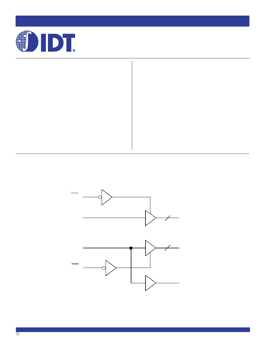
FUNCTIONAL BLOCK DIAGRAM
FEATURES:
∑ 0.5 MICRON CMOS Technology
∑ Guaranteed low skew < 500ps (max.)
∑ Very low duty cycle distortion < 600ps (max.)
∑ Low CMOS power levels
∑ TTL compatible inputs and outputs
∑ TTL level output voltage swings
∑ High drive: -32mA I
OH
, +48mA I
OL
∑ Two independent output banks with 3-state control
∑ 1:5 fanout per bank
∑ "Heartbeat" monitor output
∑ ESD > 2000V per MIL-STD-883, Method 3015; > 200V using
machine model (C = 200pF, R = 0)
∑ Available in the following packages:
≠ Commercial: QSOP, SOIC, SSOP
≠ Military: CERDIP, LCC
The IDT logo is a registered trademark of Integrated Device Technology, Inc.
IDT49FCT805BT/CT
FAST CMOS
BUFFER/CLOCK DRIVER
DESCRIPTION:
This buffer/clock driver is built using advanced dual metal CMOS
technology. The FCT805T is a non-inverting clock driver consisting of two
banks of drivers. Each bank drives five output buffers from a standard TTL
compatible input. This part has extremely low output skew, pulse skew, and
package skew. The device has a "heart-beat" monitor for diagnostics and
PLL driving. The monitor output is identical to all other outputs and complies
with the output specifications in this document.
The FCT805T is designed for fast, clean edge rates to provide accurate
clock distribution in high speed systems.
IN
A
IN
B
OE
B
OE
A
OA
1
-OA
5
OB
1
-OB
5
MON
5
5
2
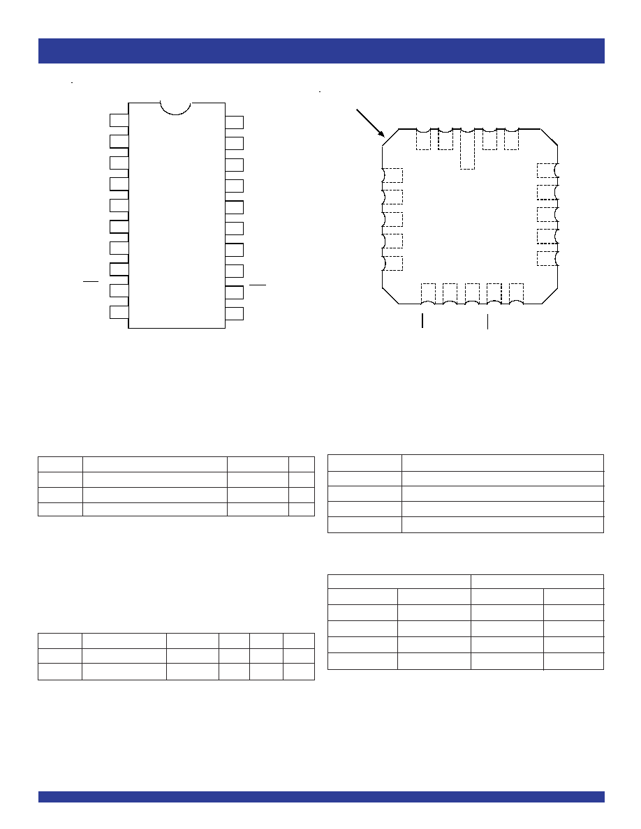
MILITARY AND COMMERCIAL TEMPERATURE RANGES
IDT49FCT805BT/CT
FAST CMOS BUFFER/CLOCK DRIVER
QSOP/ SOIC/ SSOP/ CERDIP
TOP VIEW
LCC
TOP VIEW
1
2
3
4
5
6
7
8
9
10 11 12 13
14
15
16
17
18
19
20
OA
3
OA
4
OA
5
GND
GND
(1)
OB
3
OB
4
OB
5
OB
2
GND
O
E
A
I
N
A
I
N
B
O
E
B
M
O
N
O
A
2
O
A
1
V
C
C
V
C
C
O
B
1
INDEX
V
CC
OA
1
OA
2
GND
(1)
IN
A
2
3
4
5
6
7
8
9
10
11
12
13
14
15
16
17
18
19
20
1
OA
3
OA
4
OA
5
OE
A
V
CC
OB
1
GND
MON
IN
B
OB
2
OB
3
OB
4
OB
5
OE
B
GND
NOTE:
1. Pin 8 is internally connected to GND. To insure compatibility with all products, pin
8 should be connected to GND at the board level.
PIN DESCRIPTION
Pin Names
Description
OE
A
, OE
B
3-State Output Enable Inputs (Active LOW)
IN
A
, IN
B
Clock Inputs
OAx, OBx
Clock Outputs
MON
Monitor Output
FUNCTION TABLE
(1)
Inputs
Outputs
OE
A
, OE
B
IN
A
, IN
B
OAx, OBx
MON
L
L
L
L
L
H
H
H
H
L
Z
L
H
H
Z
H
NOTE:
1. H = HIGH
L = LOW
Z = High-Impedance
PIN CONFIGURATION
ABSOLUTE MAXIMUM RATINGS
(1)
Symbol
Description
Max
Unit
V
TERM
Terminal Voltage with Respect to GND
≠0.5 to +7
V
T
STG
Storage Temperature
≠65 to +150
∞C
I
OUT
DC Output Current
≠60 to +120
mA
NOTE:
1. Stresses greater than those listed under ABSOLUTE MAXIMUM RATINGS may cause
permanent damage to the device. This is a stress rating only and functional operation
of the device at these or any other conditions above those indicated in the operational
sections of this specification is not implied. Exposure to absolute maximum rating
conditions for extended periods may affect reliability.
CAPACITANCE (T
A
= +25
O
C, f = 1.0MHz)
Symbol
Parameter
(1)
Conditions
Typ.
Max.
Unit
C
IN
Input Capacitance
V
IN
= 0V
4.5
6
pF
C
OUT
Output Capacitance
V
OUT
= 0V
5.5
8
pF
NOTE:
1. This parameter is measured at characterization but not tested.
3
IDT49FCT805BT/CT
FAST CMOS BUFFER/CLOCK DRIVER
MILITARY AND COMMERCIAL TEMPERATURE RANGES
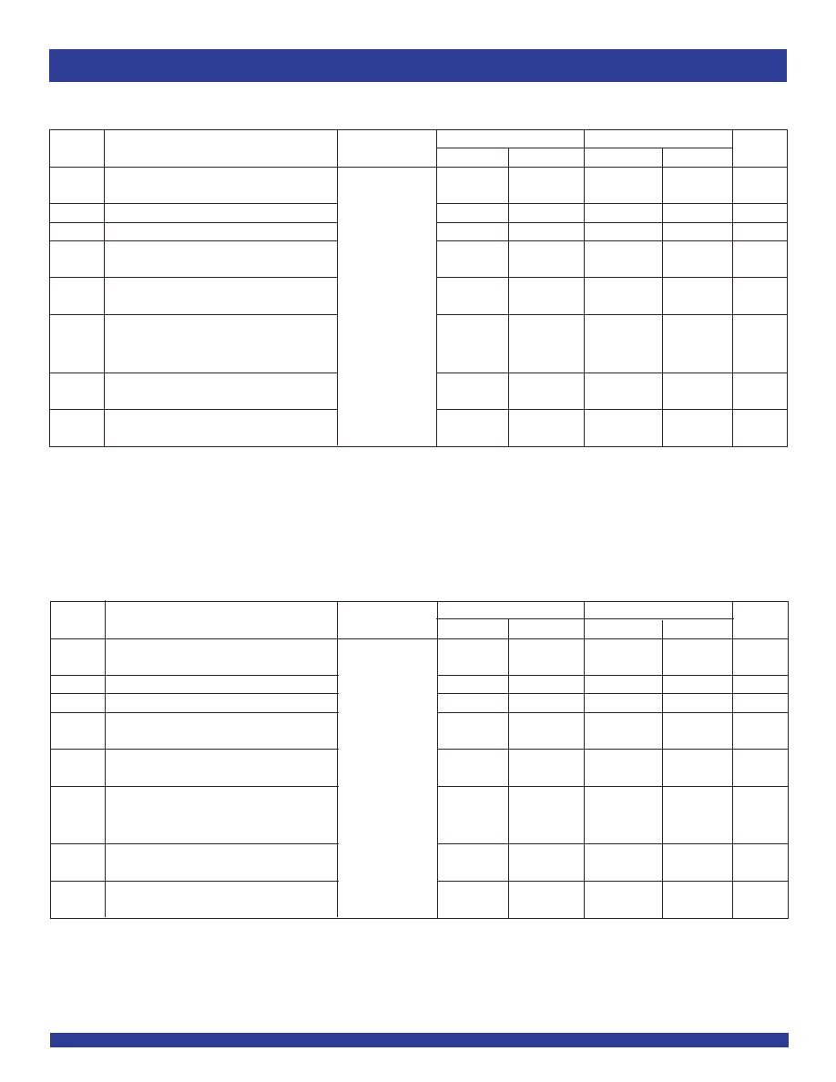
DC ELECTRICAL CHARACTERISTICS OVER OPERATING RANGE
Following Conditions Apply Unless Otherwise Specified:
Commercial: T
A
= 0∞C to +70∞C, Military: T
A
= -55∞C to +125∞C, V
CC
= 5V ± 10%
Symbol
Parameter
Test Conditions
(1)
Min.
Typ.
(2)
Max.
Unit
V
IH
Input HIGH Level
Guaranteed Logic HIGH Level
2
--
--
V
V
IL
Input LOW Level
Guaranteed Logic LOW Level
--
--
0.8
V
I
IH
Input HIGH Current
(5)
V
CC
= Max.
V
I
= 2.7V
--
--
±1
µA
I
IL
Input LOW Current
(5)
V
CC
= Max.
V
I
= 0.5V
--
--
±1
µA
I
OZH
High Impedance Output Current
V
CC
= Max.
V
O
= 2.7V
--
--
±1
µA
I
OZL
(3-State Output Pins)
V
O
= 0.5V
--
--
±1
I
I
Input HIGH Current
V
CC
= Max., V
I
= V
CC
(Max.)
--
--
±1
µA
V
IK
Clamp Diode Voltage
V
CC
= Min., I
IN
= ≠18mA
--
≠0.7
≠1.2
V
I
OS
Short Circuit Current
V
CC
= Max., V
O
= GND
(3)
≠60
≠120
≠255
mA
V
CC
= Min.
I
OH
= ≠12mA MIL
2.4
3.3
--
V
V
OH
Output HIGH Voltage
V
IN
= V
IH
or V
IL
I
OH
= ≠15mA COM'L
I
OH
= ≠24mA MIL
2
3
--
V
I
OH
= ≠32mA COM'L
(4)
V
OL
Output LOW Voltage
V
CC
= Min.
I
OL
= 32mA MIL
--
0.3
0.55
V
V
IN
= V
IH
or V
IL
I
OL
= 48mA COM'L
I
OFF
Input/Output Power Off Leakage
(5)
V
CC
= 0V, V
IN
or V
O
4.5V
--
--
±1
µA
V
H
Input Hysteresis for all inputs
--
--
150
--
mV
I
CCL
Quiescent Power Supply Current
V
CC
= Max., V
IN
= GND or V
CC
--
5
500
µA
I
CCH
I
CCZ
NOTES:
1. For conditions shown as Max. or Min., use appropriate value specified under Electrical Characteristics for the applicable device type.
2. Typical values are at Vcc = 5V, +25∞C ambient.
3. Not more than one output should be shorted at one time. Duration of the test should not exceed one second.
4. Duration of the condition should not exceed one second.
5. The test limit for this parameter is ±5
µ
A at
T
A
= -55∞C.
4
MILITARY AND COMMERCIAL TEMPERATURE RANGES
IDT49FCT805BT/CT
FAST CMOS BUFFER/CLOCK DRIVER
NOTES:
1. For conditions shown as Max. or Min., use appropriate value specified under Electrical Characteristics for the applicable device type.
2. Typical values are at V
CC
= 5V, +25∞C ambient.
3. Per TTL driven input (V
IN
= 3.4V); all other inputs at V
CC
or GND.
4. This parameter is not directly testable, but is derived for use in Total Power Supply calculations.
5. Values for these conditions are examples of the I
C
formula. These limits are guaranteed but not tested.
6.
I
C
= I
QUIESCENT
+
I
INPUTS
+ I
DYNAMIC
I
C
= I
CC
+
I
CC
D
H
N
T
+ I
CCD
(f
O
N
O
)
I
CC
= Quiescent Current (I
CCL
, I
CCH
and I
CCZ
)
I
CC
= Power Supply Current for a TTL High Input (V
I
N
= 3.4V)
D
H
= Duty Cycle for TTL Inputs High
N
T
= Number of TTL Inputs at D
H
I
CCD
= Dynamic Current Caused by an Input Transition Pair (HLH or LHL)
f
O
= Output Frequency
N
O
= Number of Outputs at f
O
All currents are in milliamps and all frequencies are in megahertz.
POWER SUPPLY CHARACTERISTICS
Symbol
Parameter
Test Conditions
(1)
Min.
Typ.
(2)
Max.
Unit
I
CC
Quiescent Power Supply Current
V
CC
= Max.
--
1
2
mA
TTL Inputs HIGH
V
IN
= 3.4V
(3)
I
CCD
Dynamic Power Supply Current
(4)
V
CC
= Max.
V
IN
= V
CC
--
60
100
µA/MHz
Outputs Open
V
IN
= GND
OE
A
= OE
B
= GND
50% Duty Cycle
I
C
Total Power Supply Current
(6)
V
CC
= Max.
V
IN
= V
CC
--
1.5
3
Outputs Open
V
IN
= GND
f
O
= 25MHz
50% Duty Cycle
V
IN
= 3.4V
--
1.8
4
OE
A
= OE
B
= V
CC
V
IN
= GND
Mon. Output Toggling
V
CC
= Max.
V
IN
= V
CC
--
33
55.5
(5)
mA
Outputs Open
V
IN
= GND
f
O
= 50MHz
50% Duty Cycle
V
IN
= 3.4V
--
33.5
57.5
(5)
OE
A
= OE
B
= GND
V
IN
= GND
Eleven Outputs Toggling
5
IDT49FCT805BT/CT
FAST CMOS BUFFER/CLOCK DRIVER
MILITARY AND COMMERCIAL TEMPERATURE RANGES
NOTES:
1. t
PLH
, t
PHL
, and t
SK
(pp) are production tested. All other parameters are guaranteed but not production tested.
2. Propagation delay range indicated by Min. and Max. limit is dues to Vcc, operating temperature, and process parameters. These propagation delay limits do not imply
skew.
3. See Test Circuits and Waveforms.
4. Minimum limits are guaranteed but not tested on Propagation Delays.
SWITCHING CHARACTERISTICS OVER OPERATING RANGE - MILITARY
(1,2)
FCT805BT
FCT805CT
Symbol
Parameter
Conditions
(3)
Min
.
(4)
Max
.
Min
.
(4)
Max
.
Unit
t
PLH
Propagation Delay
C
L
= 50pF
1.5
5.7
1.5
5.2
ns
t
PHL
IN
A
to OAx, IN
B
to OBx
R
L
= 500
t
R
Output Rise Time
--
2
--
2
ns
t
F
Output Fall Time
--
1.5
--
1.5
ns
t
SK(O)
Output skew: skew between outputs of all banks of
--
0.9
--
0.7
ns
same package (inputs tied together)
t
SK(P)
Pulse skew: skew between opposite transitions
--
0.9
--
0.8
ns
of same output (|t
PHL -≠
t
PLH
|)
t
SK(PP)
Part-to-part skew: skew between outputs of different
--
1.5
--
1.2
ns
packages at same power supply voltage,
temperature, package type and speed grade
t
PZL
Output Enable Time
1.5
6.5
1.5
6
ns
t
PZH
OE
A
to OAx, OE
B
to OBx
t
PLZ
Output Disable Time
1.5
6.5
1.5
6
ns
t
PHZ
OE
A
to OAx, OE
B
to OBx
NOTES:
1. t
PLH
, t
PHL
, and t
SK
(pp) are production tested. All other parameters are guaranteed but not production tested.
2. Propagation delay range indicated by Min. and Max. limit is dues to Vcc, operating temperature, and process parameters. These propagation delay limits do not imply
skew.
3. See Test Circuits and Waveforms.
4. Minimum limits are guaranteed but not tested on Propagation Delays.
SWITCHING CHARACTERISTICS OVER OPERATING RANGE - COMMERCIAL
(1,2)
FCT805BT
FCT805CT
Symbol
Parameter
Conditions
(3)
Min
.
(4)
Max
.
Min
.
(4)
Max
.
Unit
t
PLH
Propagation Delay
C
L
= 50pF
1.5
5
1.5
4.5
ns
t
PHL
IN
A
to OAx, IN
B
to OBx
R
L
= 500
t
R
Output Rise Time
--
1.5
--
1.5
ns
t
F
Output Fall Time
--
1.5
--
1.5
ns
t
SK(O)
Output skew: skew between outputs of all banks of
--
0.7
--
0.5
ns
same package (inputs tied together)
t
SK(P)
Pulse skew: skew between opposite transitions
--
0.7
--
0.6
ns
of same output (|t
PHL -≠
t
PLH
|)
t
SK(PP)
Part-to-part skew: skew between outputs of different
--
1.2
--
1
ns
packages at same power supply voltage,
temperature, package type and speed grade
t
PZL
Output Enable Time
1.5
6
1.5
5
ns
t
PZH
OE
A
to OAx, OE
B
to OBx
t
PLZ
Output Disable Time
1.5
6
1.5
5
ns
t
PHZ
OE
A
to OAx, OE
B
to OBx