IDT54/74FCT240/244T/AT/CT/DT - 2240/2244T/AT/CT, IDT54/74FCT540/541/2541T/AT/CT
FAST CMOS OCTAL BUFFER/LINE DRIVER
MILITARY AND COMMERCIAL TEMPERATURE RANGES
6.8
1
Integrated Device Technology, Inc.
MILITARY AND COMMERCIAL TEMPERATURE RANGES
DECEMBER 1995
©
1996 Integrated Device Technology, Inc.
6.8
DSC-2565/6
1
DESCRIPTION:
The IDT octal buffer/line drivers are built using an advanced
dual metal CMOS technology. The FCT240T/FCT2240T and
FCT244T/FCT2244T are designed to be employed as memory
and address drivers, clock drivers and bus-oriented transmit-
ter/receivers which provide improved board density.
The FCT540T and FCT541T/FCT2541T are similar in
function to the FCT240T/FCT2240T and FCT244T/FCT2244T,
respectively, except that the inputs and outputs are on oppo-
site sides of the package. This pinout arrangement makes
these devices especially useful as output ports for micropro-
cessors and as backplane drivers, allowing ease of layout and
greater board density.
The FCT2240T, FCT2244T and FCT2541T have balanced
output drive with current limiting resistors. This offers low
ground bounce, minimal undershoot and controlled output fall
times-reducing the need for external series terminating resis-
tors. FCT2xxxT parts are plug-in replacements for FCTxxxT
parts.
FAST CMOS OCTAL
BUFFER/LINE
DRIVERS
The IDT logo is a registered trademark of Integrated Device Technology, Inc.
IDT54/74FCT240T/AT/CT/DT - 2240T/AT/CT
IDT54/74FCT244T/AT/CT/DT - 2244T/AT/CT
IDT54/74FCT540T/AT/CT
IDT54/74FCT541/2541T/AT/CT
FEATURES:
∑ Common features:
≠
Low input and output leakage
1
µ
A (max.)
≠
CMOS power levels
≠
True TTL input and output compatibility
≠ V
OH
= 3.3V (typ.)
≠ V
OL
= 0.3V (typ.)
≠
Meets or exceeds JEDEC standard 18 specifications
≠
Product available in Radiation Tolerant and Radiation
Enhanced versions
≠
Military product compliant to MIL-STD-883, Class B
and DESC listed (dual marked)
≠
Available in DIP, SOIC, SSOP, QSOP, CERPACK
and LCC packages
∑ Features for FCT240T/FCT244T/FCT540T/FCT541T:
≠
Std., A, C and D speed grades
≠
High drive outputs (-15mA I
OH
, 64mA I
OL
)
∑ Features for FCT2240T/FCT2244T/FCT2541T:
≠
Std., A and C speed grades
≠
Resistor outputs
(-15mA I
OH
, 12mA I
OL
Com.)
(-12mA I
OH
, 12mA I
OL
Mil.)
≠
Reduced system switching noise
2565 drw 03
2565 drw 02
2565 drw 01
DA
0
DA
1
DA
2
DA
3
DB
0
DB
1
DB
2
DB
3
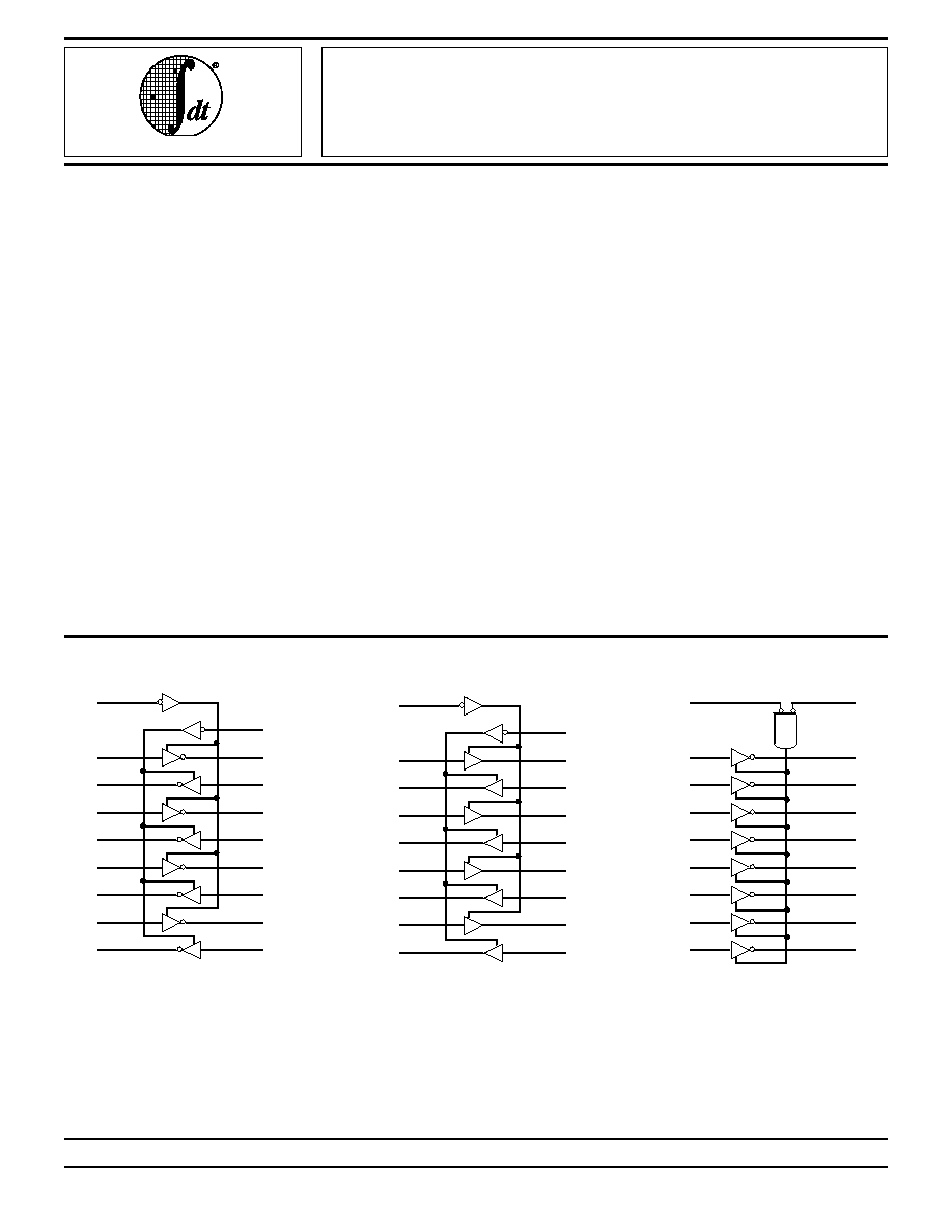
FCT240/2240T
DA
0
OB
0
DA
1
OB
1
DA
2
OB
2
DA
3
OB
3
OA
0
DB
0
OA
1
DB
1
DB
2
DB
3
OA
2
OA
3
FCT244/2244T
D
0
O
0
D
1
D
2
D
3
D
4
D
5
D
6
D
7
O
1
O
2
O
3
O
4
O
5
O
6
O
7
FCT540/541/2541T
*Logic diagram shown for 'FCT540.
'FCT541/2541T is the non-inverting option.
OE
A
OE
B
OE
A
OE
B
OE
A
OB
0
OB
1
OB
2
OB
3
OE
B
OA
0
OA
1
OA
2
OA
3
FUNCTIONAL BLOCK DIAGRAMS

IDT54/74FCT240/244T/AT/CT/DT - 2240/2244T/AT/CT, IDT54/74FCT540/541/2541T/AT/CT
FAST CMOS OCTAL BUFFER/LINE DRIVER
MILITARY AND COMMERCIAL TEMPERATURE RANGES
6.8
2
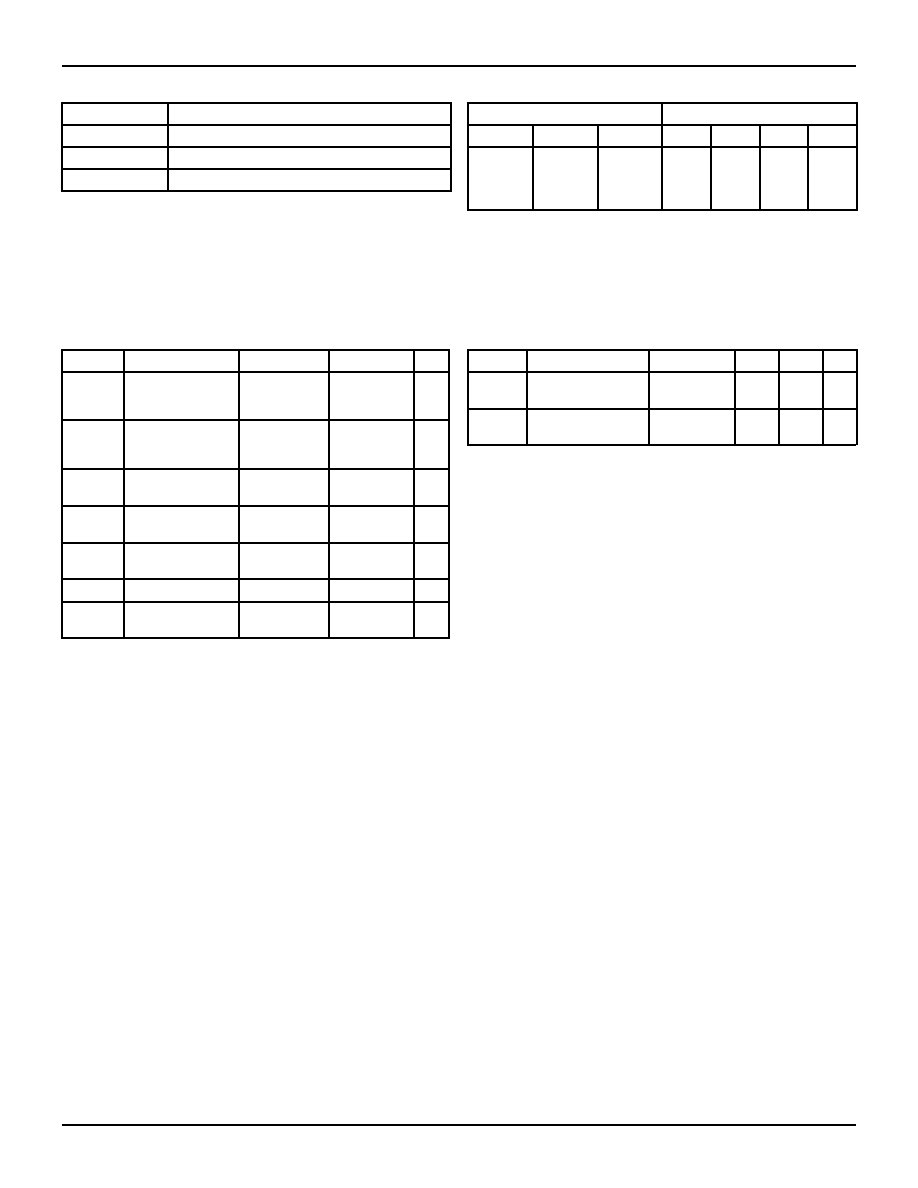
PIN CONFIGURATIONS
FCT240/2240T
FCT244/2244T
2565 drw 08
2565 drw 04
2565 drw 07
DA
0
DA
1
DA
2
DA
3
GND
DB
0
DB
1
DB
2
DB
3
V
CC
1
2
3
4
5
6
7
8
9
10
11
12
13
14
15
16
17
18
19
20
DIP/SOIC/SSOP/QSOP/CERPACK
TOP VIEW
P20-1
D20-1
SO20-2
SO20-7
SO20-8
&
E20-1
INDEX
DA
1
DA
2
DA
3
DB
0
DB
1
DA
0
OB
0
OE
A
V
CC
OE
B
OB
3
GND
DB
3
OA
3
DB
2
LCC
TOP VIEW
3
2
20 19
1
4
5
6
7
8
18
17
16
15
14
9 10 11 12 13
L20-2
OE
A
OB
0
OB
1
OB
2
OB
3
OE
B
OA
0
OA
1
OA
2
OA
3
OB
1
OB
2
OA
0
OA
1
OA
2
DA
0
OB
0
DA
1
OB
1
DA
2
OB
2
DA
3
OB
3
GND
OA
0
DB
0
OA
1
DB
1
DB
2
DB
3
OA
2
OA
3
V
CC
1
2
3
4
5
6
7
8
9
10
11
12
13
14
15
16
17
18
19
20
DIP/SOIC/SSOP/QSOP/CERPACK
TOP VIEW
P20-1
D20-1
SO20-2
SO20-7
SO20-8
&
E20-1
INDEX
DA
1
OB
1
DA
2
OB
2
DA
3
OA
0
DB
0
OA
1
DB
1
OA
2
DA
0
OB
0
V
CC
OE
B
*
OB
3
GND
DB
3
OA
3
DB
2
LCC
TOP VIEW
3
2
20 19
1
4
5
6
7
8
18
17
16
15
14
9 10
12 13
L20-2
11
OE
B
OE
A
OE
A
2565 drw 05
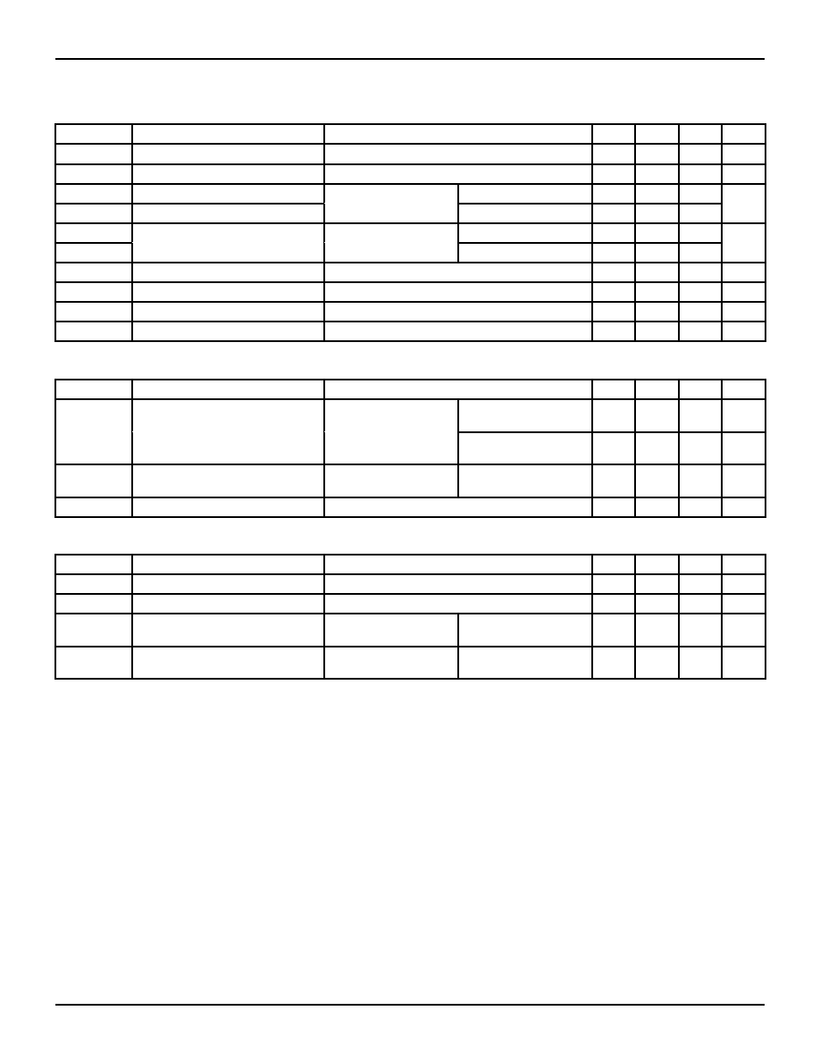
FCT540/541/2541T
D
0
D
2
D
3
D
4
D
5
D
6
D
7
GND
O
0
*
O
1
*
O
2
*
O
3
*
O
5
*
O
7
*
O
4
*
O
6
*
V
CC
1
2
3
4
5
6
7
8
9
10
11
12
13
14
15
16
17
18
19
20
DIP/SOIC/QSOP/CERPACK
TOP VIEW
P20-1
D20-1
SO20-2
SO20-8
&
E20-1
INDEX
D
2
D
3
D
4
D
5
D
6
O
0
*
O
1
*
O
2
*
O
3
*
O
4
*
LCC
TOP VIEW
3
2
20 19
1
4
5
6
7
8
18
17
16
15
14
9 10 11 12 13
L20-2
D
1
D
0
V
CC
D
7
GND
O
7
*
O
6
*
O
5
*
OE
A
OE
A
OE
B
OE
B
D
1
2565 drw 06
2565 drw 09
*
O
x for 540, Ox for 541/2541T
IDT54/74FCT240/244T/AT/CT/DT - 2240/2244T/AT/CT, IDT54/74FCT540/541/2541T/AT/CT
FAST CMOS OCTAL BUFFER/LINE DRIVER
MILITARY AND COMMERCIAL TEMPERATURE RANGES
6.8
3
PIN DESCRIPTION
FUNCTION TABLE
ABSOLUTE MAXIMUM RATINGS
(1)
CAPACITANCE
(T
A
= +25
∞
C, f = 1.0MHz)
Symbol
Rating
Commercial
Military
Unit
V
TERM(2)
Terminal Voltage
with Respect to
GND
≠0.5 to +7.0
≠0.5 to +7.0
V
V
TERM(3)
Terminal Voltage
with Respect to
GND
≠0.5 to
V
CC
+0.5
≠0.5 to
V
CC
+0.5
V
T
A
Operating
Temperature
0 to +70
≠55 to +125
∞
C
T
BIAS
Temperature
Under Bias
≠55 to +125
≠65 to +135
∞
C
T
STG
Storage
Temperature
≠55 to +125
≠65 to +150
∞
C
P
T
Power Dissipation
0.5
0.5
W
I
OUT
DC Output
Current
≠60 to +120 ≠60 to +120 mA
2565 lnk 03
NOTES:
1. Stresses greater than those listed under ABSOLUTE MAXIMUM RAT-
INGS may cause permanent damage to the device. This is a stress rating
only and functional operation of the device at these or any other conditions
above those indicated in the operational sections of this specification is
not implied. Exposure to absolute maximum rating conditions for
extended periods may affect reliability. No terminal voltage may exceed
V
CC
by +0.5V unless otherwise noted.
2. Input and V
CC
terminals only.
3. Outputs and I/O terminals only.
NOTES:
2565 tbl 02
1. H = High Voltage Level
X = Don't Care
L = Low Voltage Level
Z = High Impedance
Symbol
Parameter
(1)
Conditions
Typ.
Max. Unit
C
IN
Input
Capacitance
V
IN
= 0V
6
10
pF
C
OUT
Output
Capacitance
V
OUT
= 0V
8
12
pF
2565 lnk 04
NOTE:
1. This parameter is measured at characterization but not tested.
Pin Names
Description
OE
A
,
OE
B
3≠State Output Enable Inputs (Active LOW)
Dxx
Inputs
Oxx
Outputs
2565 tbl 01
Inputs
(1)
Outputs
(1)
OE
OE
A
OE
OE
B
D
240
244
540
541
L
L
L
H
L
H
L
L
L
H
L
H
L
H
H
H
X
Z
Z
Z
Z
IDT54/74FCT240/244T/AT/CT/DT - 2240/2244T/AT/CT, IDT54/74FCT540/541/2541T/AT/CT
FAST CMOS OCTAL BUFFER/LINE DRIVER
MILITARY AND COMMERCIAL TEMPERATURE RANGES
6.8
4
DC ELECTRICAL CHARACTERISTICS OVER OPERATING RANGE
Following Conditions Apply Unless Otherwise Specified:
Commercial: T
A
= 0
∞
C to +70
∞
C, V
CC
= 5.0V
±
5%; Military: T
A
= ≠55
∞
C to +125
∞
C, V
CC
= 5.0V
±
10%
Symbol
Parameter
Test Conditions
(1)
Min.
Typ.
(2)
Max.
Unit
V
IH
Input HIGH Level
Guaranteed Logic HIGH Level
2.0
--
--
V
V
IL
Input LOW Level
Guaranteed Logic LOW Level
--
--
0.8
V
I
I H
Input HIGH Current
(4)
V
CC
= Max.
V
I
= 2.7V
--
--
±
1
µ
A
I
I L
Input LOW Current
(4)
V
I
= 0.5V
--
--
±
1
I
OZH
High Impedance Output Current
V
CC
= Max.
V
O
= 2.7V
--
--
±
1
µ
A
I
OZL
(3-State Output pins)
(4)
V
O
= 0.5V
--
--
±
1
I
I
Input HIGH Current
(4)
V
CC
= Max., V
I
= V
CC
(Max.)
--
--
±
1
µ
A
V
IK
Clamp Diode Voltage
V
CC
= Min., I
IN
= ≠18mA
--
≠0.7
≠1.2
V
V
H
Input Hysteresis
--
--
200
--
mV
I
CC
Quiescent Power Supply Current
V
CC
= Max., V
IN
= GND or V
CC
--
0.01
1
mA
2565 lnk 05
OUTPUT DRIVE CHARACTERISTICS FOR FCT240/244/540/541T
Symbol
Parameter
Test Conditions
(1)
Min.
Typ.
(2)
Max.
Unit
V
OH
Output HIGH Voltage
V
CC
= Min.
V
IN
= V
IH
or V
IL
I
OH
= ≠6mA MIL.
I
OH
= ≠8mA COM'L.
2.4
3.3
--
V
I
OH
= ≠12mA MIL.
I
OH
= ≠15mA COM'L.
2.0
3.0
--
V
V
OL
Output LOW Voltage
V
CC
= Min.
V
IN
= V
IH
or V
IL
I
OL
= 48mA MIL.
I
OL
= 64mA COM'L.
--
0.3
0.55
V
I
OS
Short Circuit Current
V
CC
= Max., V
O
= GND
(3)
≠60
≠120
≠225
mA
2565 lnk 06
OUTPUT DRIVE CHARACTERISTICS FOR FCT2240/2244/2541T
2565 lnk 07
NOTES:
1. For conditions shown as Max. or Min., use appropriate value specified under Electrical Characteristics for the applicable device type.
2. Typical values are at Vcc = 5.0V, +25
∞
C ambient.
3. Not more than one output should be shorted at one time. Duration of the short circuit test should not exceed one second.
4. The test limit for this parameter is
±
5
µ
A at T
A
= ≠55
∞
C.
Symbol
Parameter
Test Conditions
(1)
Min.
Typ.
(2)
Max.
Unit
I
ODL
Output LOW Current
V
CC
= 5V, V
IN
= V
IH
or
V
IL,
V
OUT
= 1.5V
(3)
16
48
--
mA
I
ODH
Output HIGH Current
V
CC
= 5V, V
IN
= V
IH
or V
IL,
V
OUT
= 1.5V
(3)
≠16
≠48
--
mA
V
OH
Output HIGH Voltage
V
CC
= Min.
V
IN
= V
IH
or
V
IL
I
OH
= ≠12mA MIL.
I
OH
= ≠15mA COM'L.
2.4
3.3
--
V
V
OL
Output LOW Voltage
V
CC
= Min.
V
IN
= V
IH
or V
IL
I
OL
= 12mA
--
0.3
0.50
V
IDT54/74FCT240/244T/AT/CT/DT - 2240/2244T/AT/CT, IDT54/74FCT540/541/2541T/AT/CT
FAST CMOS OCTAL BUFFER/LINE DRIVER
MILITARY AND COMMERCIAL TEMPERATURE RANGES
6.8
5
POWER SUPPLY CHARACTERISTICS
Symbol
Parameter
Test Conditions
(1)
Min.
Typ.
(2)
Max.
Unit
I
CC
Quiescent Power Supply Current
TTL Inputs HIGH
V
CC
= Max.
V
IN
= 3.4V
(3)
--
0.5
2.0
mA
I
CCD
Dynamic Power Supply
Current
(4)
V
CC
= Max.
Outputs Open
OE
A
=
OE
B
= GND
V
IN
= V
CC
V
IN
= GND
FCTxxxT
--
0.15
0.25
mA/
MHz
One Input Toggling
50% Duty Cycle
FCT2xxxT
--
0.06
0.12
I
C
Total Power Supply Current
(6)
V
CC
= Max.
V
IN
= V
CC
FCTxxxT
--
1.5
3.5
mA
Outputs Open
fi = 10MHz
V
IN
= GND FCT2xxxT
--
0.6
2.2
50% Duty Cycle
OE
A
=
OE
B
= GND
V
IN
= 3.4
FCTxxxT
--
1.8
4.5
One Bit Toggling
V
IN
= GND FCT2xxxT
0.9
3.2
V
CC
= Max.
V
IN
= V
CC
FCTxxxT
--
3.0
6.0
(5)
Outputs Open
fi = 2.5MHz
V
IN
= GND FCT2xxxT
--
1.2
3.4
(5)
50% Duty Cycle
OE
A
=
OE
B
= GND
V
IN
= 3.4
FCTxxxT
--
5.0
14.0
(5)
Eight Bits Toggling
V
IN
= GND FCT2xxxT
--
3.2
11.4
(
5)
NOTES:
1. For conditions shown as Max. or Min., use appropriate value specified under Electrical Characteristics for the applicable device type.
2. Typical values are at V
CC
= 5.0V, +25
∞
C ambient.
3. Per TTL driven input (V
IN
= 3.4V). All other inputs at V
CC
or GND.
4. This parameter is not directly testable, but is derived for use in Total Power Supply Calculations.
5. Values for these conditions are examples of the I
CC
formula. These limits are guaranteed but not tested.
6. I
C
= I
QUIESCENT
+ I
INPUTS
+ I
DYNAMIC
I
C
= I
CC
+
I
CC
D
H
N
T
+ I
CCD
(f
CP/
2 + f
i
N
i
)
I
CC
= Quiescent Current
I
CC
= Power Supply Current for a TTL High Input (V
IN
= 3.4V)
D
H
= Duty Cycle for TTL Inputs High
N
T
= Number of TTL Inputs at D
H
I
CCD
= Dynamic Current Caused by an Input Transition Pair (HLH or LHL)
f
CP
= Clock Frequency for Register Devices (Zero for Non-Register Devices)
f
i
= Input Frequency
N
i
= Number of Inputs at f
i
All currents are in milliamps and all frequencies are in megahertz.
2565 tbl 08