MILITARY AND COMMERCIAL TEMPERATURE RANGES
AUGUST 1996
©
1996 Integrated Device Technology, Inc.
5.11
DSC≠2916/5
Integrated Device Technology, Inc.
The IDT logo is a registered trademark of Integrated Device Technology, Inc.
FAST CMOS 16-BIT
REGISTERED/LATCHED
TRANSCEIVER WITH PARITY
IDT54/74FCT162511AT/CT
FEATURES:
∑ 0.5 MICRON CMOS Technology
∑ Typical tsk(o) (Output Skew) < 250ps, clocked mode
∑ Low input and output leakage
1
µ
A (max)
∑ ESD > 2000V per MIL-STD-883, Method 3015;
> 200V using machine model (C = 200pF, R = 0)
∑ Packages include 25 mil pitch SSOP, 19.6 mil pitch TSSOP,
15.7 mil pitch TVSOP and 25 mil pitch Cerpack
∑ Extended commercial range of ≠40
∞
C to +85
∞
C
∑ V
CC
= 5V
±
10%
∑ Balanced Output Drivers:
±
24mA (commercial)
±
16mA (military)
∑ Series current limiting resistors
∑ Generate/Check, Check/Check modes
∑ Open drain parity error allows wire-OR
DESCRIPTION:
The FCT162511AT/CT 16-bit registered/latched transceiver
with parity is built using advanced dual metal CMOS technol-
ogy. This high-speed, low-power transceiver combines D-
type latches and D-type flip-flops to allow data flow in transpar-
ent, latched or clocked modes. The device has a parity
generator/cheker in the A-to-B direction and a parity checker
in the B-to-A direction. Error checking is done at the byte level
with separate parity bits for each byte. Separate error flags
exits for each direction with a single error flag indicating an
error for either byte in the A-to-B direction and a second error
flag indicating an error for either byte in the B-to-A direction.
The parity error flags are open drain outputs which can be tied
together and/or tied with flags from other devices to form a
single error flag or interrupt. The parity error flags are enabled
by the
OExx
control pins allowing the designer to disable the
error flag during combinational transitions.
The control pins LEAB, CLKAB and
OEAB
control opera-
tion in the A-to-B direction while LEBA, CLKBA and
OEBA
control the B-to-A direction.
GEN
/CHK is only for the selection
of A-to-B operation, the B-to-A direction is always in checking
mode. The ODD/
EVEN
select is common between the two
directions. Except for the ODD/
EVEN
control, independent
operation can be achieved between the two directions by
using the corresponding control lines.
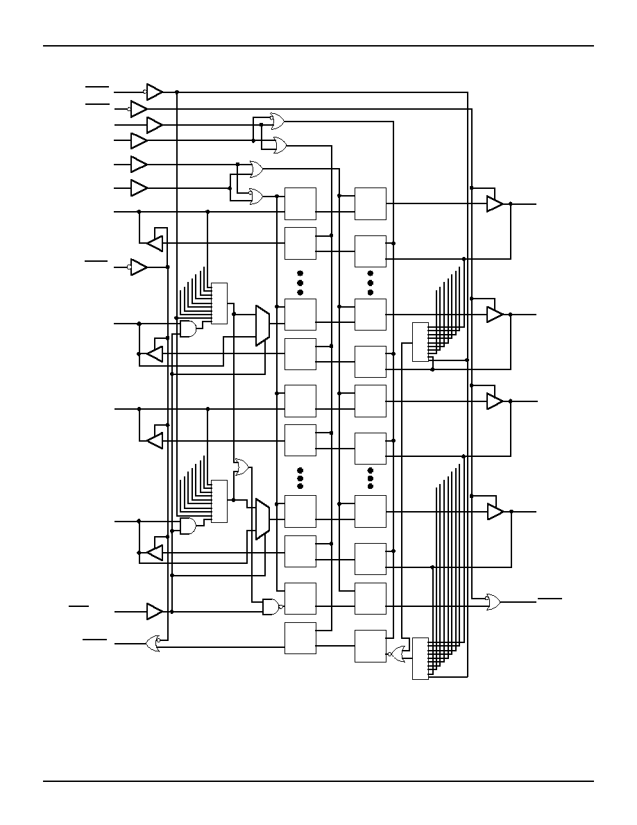
SIMPLIFIED FUNCTIONAL BLOCK DIAGRAM:
GEN/CHK
Latch/
Register
Byte
Parity
Generator/
Checker
Latch/
Register
Byte
Parity
Checking
B0-15
A0-15
PA1,2
PB1,2
PERB
LEAB
CLKAB
OEAB
OEBA
PERA
LEBA
CLKBA
Parity, data
Parity, data
Parity, Data
Data
(Open Drain)
(Open Drain)
Parity
ODD/EVEN
16
18
18
18
2
2916 drw 01
1

5.11
2
IDT54/74FCT162511AT/CT
FAST CMOS 16-BIT REGISTERED/LATCHED TRANSCEIVER WITH PARITY
MILITARY AND COMMERCIAL TEMPERATURE RANGES
FUNCTIONAL BLOCK DIAGRAM
A
8
- A
15
GEN/CHK
OEAB
CLKBA
LEBA
CLKAB
A
0
- A
7
LEAB
B
0
- B
7
D
C
C
D
OEBA
D
C
B
8
- B
15
D
C
C
D
PB
2
PA
2
C
D
C
D
P
C
D
C
D
PERB
D
C
D
C
PB
1
PA
1
C
D
C
D
P
(Open Drain)
D
C
D
C
D
C
D
C
D
C
D
C
D
C
ODD/EVEN
(Open Drain)
PERA
P
P
I
O
I
O
2916 drw 02

IDT54/74FCT162511AT/CT
FAST CMOS 16-BIT REGISTERED/LATCHED TRANSCEIVER WITH PARITY
MILITARY AND COMMERCIAL TEMPERATURE RANGES
5.11
3
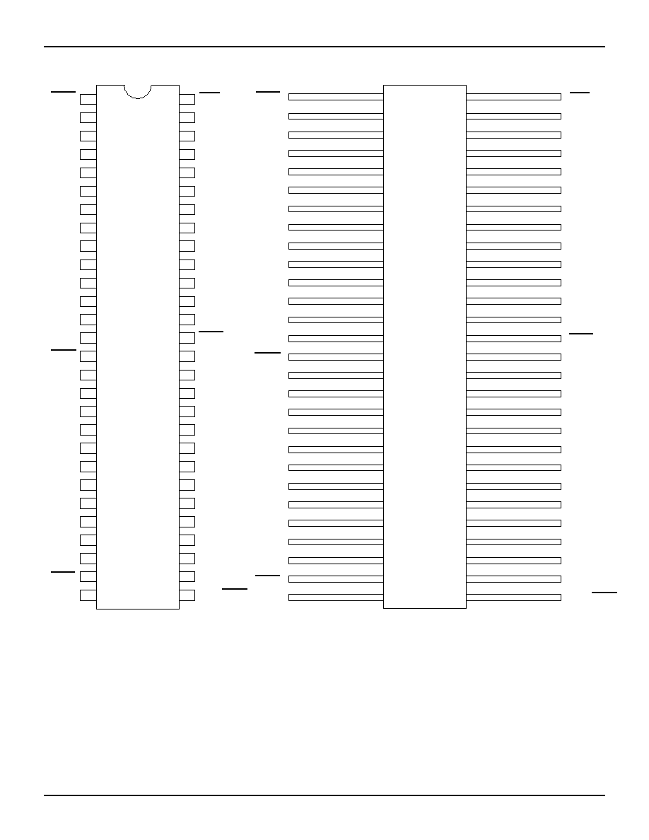
PIN CONFIGURATIONS
2916 drw 03
2916 drw 04
OEAB
LEAB
PA
1
GND
A
0
A
1
V
CC
A
2
A
3
A
5
A
4
A
6
A
7
GND
A
10
PERA
A
8
V
CC
A
9
PA
2
A
12
A
11
A
14
GND
A
15
LEBA
A
13
GEN/CHK
B
0
B
1
GND
B
2
B
3
V
CC
B
4
B
6
PB
1
B
7
PERB
GND
B
8
B
5
B
9
B
11
V
CC
B
12
B
10
CLKAB
B
14
B
13
B
15
GND
PB
2
CLKBA
ODD/EVEN
OEBA
47
37
38
39
40
41
42
43
44
45
46
33
34
35
36
56
55
49
50
51
52
53
54
48
1
2
3
4
5
6
7
8
9
10
12
13
14
15
16
17
18
19
20
11
21
22
23
24
29
30
31
32
25
26
27
28
CERPACK
TOP VIEW
E56-1
GEN/CHK
B
0
B
1
GND
B
2
B
3
V
CC
B
4
B
6
PB
1
B
7
PERB
GND
B
8
B
5
B
9
B
11
V
CC
B
12
B
10
CLKAB
B
14
B
13
B
15
GND
PB
2
CLKBA
ODD/EVEN
OEAB
LEAB
PA
1
GND
A
0
A
1
V
CC
A
2
A
3
A
5
A
4
A
6
A
7
GND
A
10
PERA
A
8
V
CC
A
9
PA
2
A
12
A
11
A
14
GND
A
15
LEBA
A
13
OEBA
47
37
38
39
40
41
42
43
44
45
46
33
34
35
36
56
55
49
50
51
52
53
54
48
1
2
3
4
5
6
7
8
9
10
12
13
14
15
16
17
18
19
20
11
21
22
23
24
SSOP/
TSSOP/TVSOP
TOP VIEW
SO56-1
SO56-2
SO56-3
29
30
31
32
25
26
27
28

5.11
4
IDT54/74FCT162511AT/CT
FAST CMOS 16-BIT REGISTERED/LATCHED TRANSCEIVER WITH PARITY
MILITARY AND COMMERCIAL TEMPERATURE RANGES
ABSOLUTE MAXIMUM RATINGS
(1)
PIN DESCRIPTION
Pin Names
Description
OEAB
A-to-B Output Enable Input (Active LOW)
OEBA
B-to-A Output Enable Input (Active LOW)
LEAB
A-to-B Latch Enable Input
LEBA
B-to-A Latch Enable Input
CLKAB
A-to-B Clock Input
CLKBA
B-to-A Clock Input
Ax
A-to-B Data Inputs or B-to-A 3-State Outputs
Bx
B-to-A Data Inputs or A-to-B 3-State Outputs
PERA
Parity Error (Open Drain) on A Outputs
PERB
Parity Error (Open Drain) on B Outputs
PAx
(1)
A-to-B Parity Input, B-to-A Parity Output
PBx
B-to-A Parity Input, A-to-B Parity Output
ODD/
EVEN
Parity Mode Selection Input
GEN
/CHK
A to B Port Generate or Check Mode Input
2916 tbl 03
NOTES:
1. The PAx pin input is internally disabled during parity generation. This
means that when generating parity in the A to B direction there is no need
to add a pull up resistor to guarantee state. The pin will still function
properly as the parity output for the B to A direction.
Symbol
Description
Max.
Unit
V
TERM(2)
Terminal Voltage with Respect to
GND
≠0.5 to +7.0
V
V
TERM(3)
Terminal Voltage with Respect to
GND
≠0.5 to
V
CC
+0.5
V
T
STG
Storage Temperature
≠65 to +150
∞
C
I
OUT
DC Output Current
≠60 to +120 mA
NOTES:
1. Stresses greater than those listed under ABSOLUTE MAXIMUM RAT-
INGS may cause permanent damage to the device. This is a stress rating
only and functional operation of the device at these or any other conditions
above those indicated in the operational sections of this specification is
not implied. Exposure to absolute maximum rating conditions for
extended periods may affect reliability.
2. Open drain and all device terminals except FCT162XXXT Output and I/O
terminals.
3. Output and I/O terminals for FCT162XXXT.
2916 lnk 01
FUNCTION TABLE
(1,4)
Inputs
Outputs
OEAB
OEAB
LEAB
CLKAB
Ax
Bx
H
X
X
X
Z
L
H
X
L
L
L
H
X
H
H
L
L
L
L
L
L
H
H
L
L
L
X
B
(2)
L
L
H
X
B
(3)
NOTES:
2916 tbl 02
1. A-to-B data flow is shown. B-to-A data flow is similar but uses
OEBA
,
LEBA, and CLKBA.
2. Output level before the indicated steady-state input conditions were
established.
3. Output level before the indicated steady-state input conditions were
established, provided that CLKAB was HIGH before LEAB went LOW.
4. H = HIGH Voltage Level
L = LOW Voltage Level
X = Don't Care
Z = High Impedance
= LOW-to-HIGH Transition

IDT54/74FCT162511AT/CT
FAST CMOS 16-BIT REGISTERED/LATCHED TRANSCEIVER WITH PARITY
MILITARY AND COMMERCIAL TEMPERATURE RANGES
5.11
5
NOTE:
1. This parameter is measured at characterization but not tested.
CAPACITANCE
(T
A
= +25
∞
C, f = 1.0MHz)
2916 lnk 04
NOTES:
1. Conditions shown are for
GEN
/CHK = H,
OEAB
= L,
OEBA
= H.
2. A-to-B parity checking is shown. B-to-A parity checking is similar but uses
OEBA
= L,
OEAB
= H and errors will be indicated on
PERA
.
3. In parity checking mode the parity bits will be transmitted unchanged along
with the corresponding data regardless of parity errors. (PB
1
= PA
1
).
4. The response shown is for LEAB = H. If LEAB = L then CLKAB will control
as an edge triggered clock.
5. Conditions shown are for the byte A
0
-A
7
and PA
1
. The byte A
8
-A
15
and
PA
2
is similiar.
6. The parity error flag
PERB
is a combined flag for both bytes A
0
-A
7
and A
8
-
A
15
. If a parity error occurs on either byte
PERB
will go low.
PERB
is an
open drain output which must be externally pulled up to achieve a logic
HIGH.
FUNCTION TABLE
(PARITY CHECKING)
(1, 2, 3, 4)
FUNCTION TABLE
(PARITY GENERATION)
(1, 2, 3, 4, 5)
2916 tbl 05
2916 tbl 06
NOTES:
1. Conditions shown are for
GEN
/CHK = L,
OEAB
= L,
OEBA
= H.
2. A-to-B parity checking is shown. B-to-A is capable of parity checking while
A-to-B is performing generation. B-to-A will not generate parity.
3. The response shown is for LEAB = H. If LEAB = L then CLKAB will control
as an edge triggered clock.
4. Conditions shown are for the byte A
0
-A
7
. The byte A
8
-A
15
is similiar but
will output the parity on PB
2
.
5. The error flag
PERB
will remain in a high state during parity generation.
Symbol
Parameter
(1)
Conditions
Typ.
Max.
Unit
C
IN
Input
Capacitance
V
IN
= 0V
3.5
6.0
pF
C
I/O
I/O
Capacitance
V
OUT
= 0V
3.5
8.0
pF
C
O
Open Drain
Capacitance
V
OUT
= 0V
3.5
6.0
pF
A
0
- A
7
, Total Number
of inputs that are high
ODD/
EVEN
EVEN
PB
1
1, 3, 5 or 7
L
H
1, 3, 5 or 7
H
L
0, 2, 4, 6 or 8
L
L
0, 2, 4, 6 or 8
H
H
A
0
- A
7
and PA
1(5)
, Total Number
of inputs that are high
ODD/
EVEN
EVEN
PERB
PERB
1, 3, 5, 7 or 9
L
L
1, 3, 5, 7 or 9
H
H
(6)
0, 2, 4, 6 or 8
L
H
(6)
0, 2, 4, 6 or 8
H
L


