
1
IDT74FCT162701T/AT
FAST CMOS 18-BIT READ/WRITE BUFFER
INDUSTRIAL TEMPERATURE RANGE
JANUARY 2002
© 2002 Integrated Device Technology, Inc.
DSC-2915/1
IDT74FCT162701T/AT
INDUSTRIAL TEMPERATURE RANGE
FAST CMOS 18-BIT
READ/WRITE BUFFER
DESCRIPTION:
The FCT162701T is an 18-bit Read/Write buffer with a four deep FIFO and
a read-back latch. It can be used as a read/write buffer between a CPU and
memory or to interface a high-speed bus and a slow peripheral. The A-to-B
(write) path has a four deep FIFO for pipelined operations. The FIFO can be
reset and a FIFO full condition is indicated by the full flag (FF). The B-to-A (read)
path has a latch. A high on LE, allows data to flow transparently from B-to-A.
A low on LE allows the data to be latched on the falling edge of LE.
The FCT162701T has a balanced output drive with series termination.
This provides low ground bounce, minimal undershoot and controlled output
edge rates.
FUNCTIONAL BLOCK DIAGRAM
LATCH
LE
O EBA
18
18
A
1-18
B
1-18
FIFO
(4 deep)
OEA B
FF
CLK
RESE T
W CE
RCE
FEATURES:
∑ 0.5 MICRON CMOS Technology
∑ Typical t
SK
(o) (Output Skew) < 250ps
∑ Low input and output leakage
1µA (max.)
∑ ESD > 2000V per MIL-STD-883, Method 3015; > 200V using
machine model (C = 200pF, R = 0)
∑ Balanced Output Drivers (±24mA)
∑ Reduced system switching noise
∑ Typical V
OLP
(Output Ground Bounce) < 0.6V at V
CC
= 5V,
T
A
= 25∞C
∑ Ideal for new generation x86 write-back cache solutions
∑ Suitable for modular x86 architectures
∑ Four deep write FIFO
∑ Latch in read path
∑ Synchronous FIFO reset
∑ Available in SSOP and TSSOP packages
The IDT logo is a registered trademark of Integrated Device Technology, Inc.
2
INDUSTRIAL TEMPERATURE RANGE
IDT74FCT162701T/AT
FAST CMOS 18-BIT READ/WRITE BUFFER
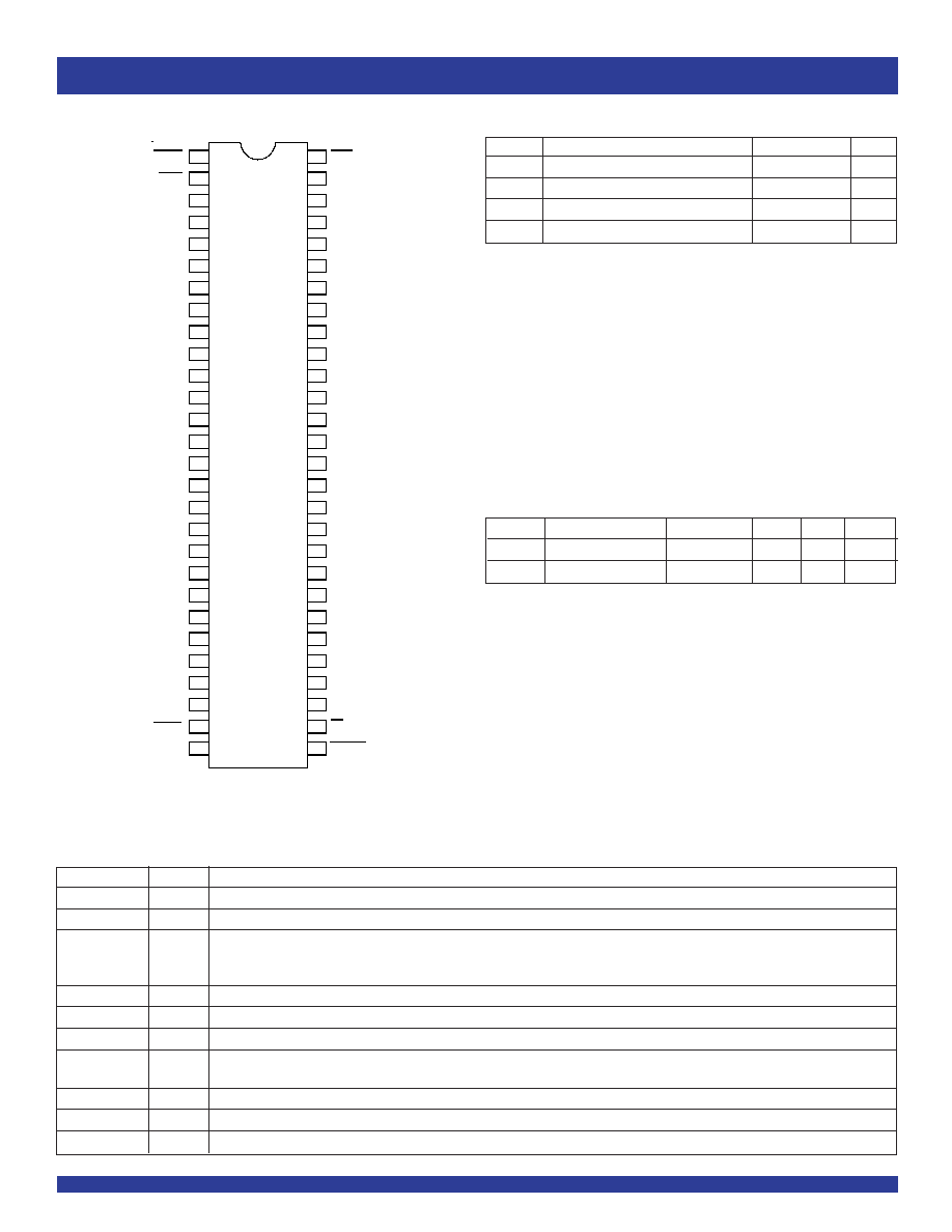
SSOP/ TSSOP
TOP VIEW
PIN CONFIGURATION
RCE
B
2
B
3
GND
B
4
B
5
V
CC
B
6
B
7
B
1
B
8
B
9
B
10
B
11
GND
B
12
B
13
V
CC
B
14
GND
CLK
B
16
B
15
B
17
GND
B
18
FF
RESET
OEA B
W CE
A
1
GND
A
2
A
3
V
C C
A
4
A
5
A
9
A
6
A
7
A
8
GND
GND
A
10
A
11
V
C C
A
12
A
18
A
14
A
13
A
16
GND
A
17
LE
A
15
OEB A
47
37
38
39
40
41
42
43
44
45
46
33
34
35
36
56
55
49
50
51
52
53
54
48
1
2
3
4
5
6
7
8
9
10
12
13
14
15
16
17
18
19
20
11
21
22
23
24
29
30
31
32
25
26
27
28
Symbol
Description
Max
Unit
V
TERM
(2)
Terminal Voltage with Respect to GND
≠0.5 to 7
V
V
TERM
(3)
Terminal Voltage with Respect to GND
≠0.5 to V
CC
+0.5
V
T
STG
Storage Temperature
≠65 to +150
∞C
I
OUT
DC Output Current
≠60 to +120
mA
ABSOLUTE MAXIMUM RATINGS
(1)
(1)
(1)
(1)
(1)
NOTES:
1. Stresses greater than those listed under ABSOLUTE MAXIMUM RATINGS may cause
permanent damage to the device. This is a stress rating only and functional operation
of the device at these or any other conditions above those indicated in the operational
sections of this specification is not implied. Exposure to absolute maximum rating
conditions for extended periods may affect reliability.
2. All device terminals except FCT162XXX Output and I/O terminals.
3. Output and I/O terminals for FCT162XXX.
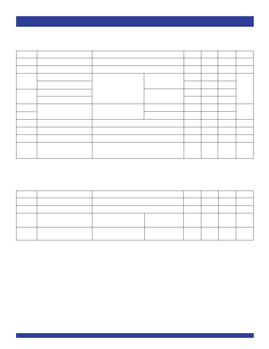
Symbol
Parameter
(1)
Conditions
Typ.
Max.
Unit
C
IN
Input Capacitance
V
IN
= 0V
3.5
6
pF
C
OUT
Output Capacitance
V
OUT
= 0V
3.5
8
pF
CAPACITANCE
(T
A
= +25∞C, f = 1.0MHz)
NOTE:
1. This parameter is measured at characterization but not tested.
PIN DESCRIPTION
Pin Names
I/O
Description
A
1-18
I/O
18 bit I/O port
B
1-18
I/O
18 bit I/O port
CLK
I
Clock for write path FIFO. Clocks data into FIFO when WCE is low, clocks data out of FIFO when RCE is low. When FIFO is full
all further writes to the FIFO are inhibited. When FIFO is empty all reads from the FIFO are inhibited. CLK also resets the FIFO when
RESET is low.
WCE
I
Enable pin for FIFO input clock
RCE
I
Enable pin for FIFO output clock
FF
O
Write path FIFO full flag. Goes low when FIFO is full.
RESET
I
Synchronous FIFO reset - when low CLK resets the FIFO. The FIFO pointers are initialized to the "empty" condition and FIFO output
is forced high (all ones). The FIFO full flag (FF) will be high immediately after reset.
OEAB
I
Output Enable pin for B port
OEBA
I
Output Enable pin for A port
LE
I
Read path latch enable pin. When high, data flows transparently from B port to A port, B data is latched on the falling edge of LE.

3
IDT74FCT162701T/AT
FAST CMOS 18-BIT READ/WRITE BUFFER
INDUSTRIAL TEMPERATURE RANGE
FUNCTIONAL DESCRIPTION
This device is useful as a read/write buffer for modular high end designs. It
provides multi-level buffering in the write path and single deep buffering in the
read path, and is suited to write back cache implementation. The read path
provides a transparent latch.
The four deep FIFO uses one clock with two clock enable pins, WCE and
RCE to clock data in and out. The FIFO has an external full flag which goes
LOW when the FIFO is full. Internal read and write pointers keep track of the
words stored in the FIFO. A write attempt to a full FIFO is ignored. An attempt
to read from an empty FIFO will have no effect and the last read data remains
at the output of the FIFO. The FIFO may be reset by the synchronous RESET
input. This resets the read and write pointers to the original "empty" condition
and also sets all B outputs = 1. Simultaneous read and write attempts (clock data
into FIFO as well as clock data out of FIFO) are possible except on FIFO empty
and full boundaries. When the FIFO is empty, and a simultaneous read and
write is attempted, the read is ignored while the write is executed. If the same
is attempted when the FIFO is full, the write is ignored while the read is executed.
Normal operation of the four deep FIFO in the write path is independent of the
read path operation.
Power, ground and data pin positions on the FCT162701T match those on
the FCT16501T/162501T, allowing an easy upgrade.
APPLICATIONS--486 INTERFACE
Figure 1. FCT162701T Application Example
i486
FCT162701T
CacheRAM
PAL
CLK,W CE,
RCE, RST
CLK
W /R
LE,O EBA,
OEAB
DRAM
Coprocessor
A
B
4
INDUSTRIAL TEMPERATURE RANGE
IDT74FCT162701T/AT
FAST CMOS 18-BIT READ/WRITE BUFFER
Symbol
Parameter
Test Conditions
(1)
Min.
Typ.
(2)
Max.
Unit
V
IH
Input HIGH Level
Guaranteed Logic HIGH Level
2
--
--
V
V
IL
Input LOW Level
Guaranteed Logic LOW Level
--
--
0.8
V
I
IH
Input HIGH Current (Input pins)
(4)
V
CC
= Max.
V
I
= V
CC
--
--
±1
µA
Input HIGH Current (I/O pins)
(4)
--
--
±1
I
IL
Input LOW Current (Input pins)
(4)
V
I
= GND
--
--
±1
Input LOW Current (I/O pins)
(4)
--
--
±1
I
OZH
High Impedance Output Current
V
CC
= Max.
V
O
= 2.7V
--
--
±1
µA
I
OZL
(3-State Output pins)
(4)
V
O
= 0.5V
--
--
±1
V
IK
Clamp Diode Voltage
V
CC
= Min., I
IN
= ≠18mA
--
≠0.7
≠1.2
V
I
OS
Short Circuit Current
V
CC
= Max., V
O
= GND
(3)
≠80
≠140
≠250
mA
V
H
Input Hysteresis
--
--
100
--
mV
I
CCL
Quiescent Power Supply Current
V
CC
= Max.
--
5
500
µA
I
CCH
V
IN
= GND or V
CC
I
CCZ
NOTES:
1. For conditions shown as Min. or Max., use appropriate value specified under Electrical Characteristics for the applicable device type.
2. Typical values are at V
CC
= 5.0V, +25∞C ambient.
3. Not more than one output should be shorted at one time. Duration of the test should not exceed one second.
4. The test limit of this parameter is ±5µA at T
A
= ≠55∞C.
DC ELECTRICAL CHARACTERISTICS OVER OPERATING RANGE
Following Conditions Apply Unless Otherwise Specified:
Industrial: T
A
= ≠40∞C to +85∞C, V
CC
= 5.0V ±10%
Symbol
Parameter
Test Conditions
(1)
Min.
Typ.
(2)
Max.
Unit
I
ODL
Output LOW Current
V
CC
= 5V, V
IN
= V
IH
or V
IL
, V
O
= 1.5V
(3)
60
115
200
mA
I
ODH
Output HIGH Current
V
CC
= 5V, V
IN
= V
IH
or V
IL
, V
O
= 1.5V
(3)
≠60
≠115
≠200
mA
V
OH
Output HIGH Voltage
V
CC
= Min.
I
OH
= ≠24mA
2.4
3.3
--
V
V
IN
= V
IH
or V
IL
V
OL
Output LOW Voltage
V
CC
= Min.
I
OL
= 24mA
--
0.3
0.55
V
V
IN
= V
IH
or V
IL
OUTPUT DRIVE CHARACTERISTICS

5
IDT74FCT162701T/AT
FAST CMOS 18-BIT READ/WRITE BUFFER
INDUSTRIAL TEMPERATURE RANGE
NOTES:
1. For conditions shown as Min. or Max., use appropriate value specified under Electrical Characteristics for the applicable device type.
2. Typical values are at V
CC
= 5.0V, +25∞C ambient.
3. Per TTL driven input (V
IN
= 3.4V). All other inputs at V
CC
or GND.
4. This parameter is not directly testable, but is derived for use in Total Power Supply Calculations.
5. Values for these conditions are examples of the I
CC
formula. These limits are guaranteed but not tested.
6. I
C
= I
QUIESCENT
+ I
INPUTS
+ I
DYNAMIC
I
C
= I
CC
+
I
CC
D
H
N
T
+ I
CCD (CLK)
x f
CP
+ I
CCD (O/P)
x f
O
N
O
I
CC
= Quiescent Current (I
CCL
, I
CCH
and I
CCZ
)
I
CC
= Power Supply Current for a TTL High Input (V
IN
= 3.4V)
D
H
= Duty Cycle for TTL Inputs High
N
T
= Number of TTL Inputs at D
I
CCD
= Dynamic Current Caused by an Input Transition Pair (HLH or LHL)
f
CP
= Clock Frequency for Register Devices (Zero for Non-Register Devices)
f
O
= Output Frequency
N
O
= Number of Outputs at f
O
Symbol
Parameter
Test Conditions
(1)
Min.
Typ.
(2)
Max.
Unit
I
CC
Quiescent Power Supply Current
V
CC
= Max.
--
0.5
1.5
µA
TTL Inputs HIGH
V
IN
= 3.4V
(3)
I
CCD (CLK)
Dynamic Power Supply Current
V
CC
= Max.
CLK Toggling
V
IN
= V
CC
--
180
240
µA/
due to clock switching
(4)
Outputs Open
50% Duty Cycling
V
IN
= GND
MHz
I
CCD (O/P)
Dynamic Power Supply Current
One Input Toggling
--
80
120
due to clock switching
(4)
50% Duty Cycle
I
C
Total Power Supply Current
(6)
V
CC
= Max.
V
IN
= V
CC
--
1.8
2.9
(5)
mA
Outputs Open
V
IN
= GND
f
CP
= 10MHz
50% Duty Cycle
OEAB = GND; OEBA = V
CC
V
IN
= 3.4V
--
2.1
3.7
(5)
LE = WCE = RCE = GND
V
IN
= GND
RESET = V
CC
All Inputs Low
V
CC
= Max.
V
IN
= V
CC
--
2.2
3.5
Outputs Open
V
IN
= GND
f
CP
= 10MHz
50% Duty Cycle
OEAB = GND; OEBA = V
CC
V
IN
= 3.4V
--
2.7
5
LE = WCE = RCE = GND
V
IN
= GND
RESET = V
CC
One Bit Toggling
at f
O
= 5MHz
50% Duty Cycle
POWER SUPPLY CHARACTERISTICS
6
INDUSTRIAL TEMPERATURE RANGE
IDT74FCT162701T/AT
FAST CMOS 18-BIT READ/WRITE BUFFER
NOTES:
1. See test circuit and waveforms.
2. Minimum limits are guaranteed but not tested on Propagation Delays.
3. Guaranteed but not tested.
SWITCHING CHARACTERISTICS OVER OPERATING RANGE
FCT162701T
FCT162701AT
Parameter
Test Conditions
(1)
Min.
(2)
Max.
(2)
Min.
(2)
Max.
(2)
Unit
PROPAGATION DELAYS
1
B
1-18
to A
1-18
Read path/latch
1.5
6.5
1.5
5.5
ns
2
LE (LOW to HIGH) to A
1-18
Read path/latch
1.5
5.7
1.5
4.7
ns
3
CLK to FF
Write path
2
7
2
6
ns
4
CLK to B
1-18
Write path
1
6
1
5.2
ns
SETUP & HOLD TIMES
(3)
5
A
1-18
to CLK (LOW to HIGH) Setup
Write path
2.5
--
2.5
--
ns
6
A
1-18
to CLK (LOW to HIGH) Hold
Write path
0
--
0
--
ns
7
B
1-18
to LE (HIGH to LOW) Setup
Read path/latch
3
--
3
--
ns
8
B
1-18
to LE (HIGH to LOW) Hold
Read path/latch
0
--
0
--
ns
9
WCE, RCE (LOW) to CLK Setup
Write path
3
--
3
--
ns
10
WCE, RCE (LOW) to CLK Hold
Write path
0
--
0
--
ns
11
RESET (LOW) to CLK Setup
Write path
3
--
3
--
ns
12
RESET (LOW) to CLK Hold
Write path
0
--
0
--
ns
ENABLE & DISABLE TIMES
(3)
13
OEBA LOW to A
1-18
Enable
Write path
1.5
7
1.5
6
ns
14
OEBA HIGH to A
1-18
Disable
Write path
1.5
6
1.5
5
ns
15
OEAB LOW to B
1-18
Enable
Read path
1.5
7
1.5
6
ns
16
OEAB HIGH to B
1-18
Disable
Read path
1.5
6
1.5
5
ns
MINIMUM PULSE WIDTHS
17
CLK HIGH or LOW Pulse Width
Write path
3
--
3
--
ns
18
LE HIGH Pulse Width
Read path/latch
3
--
3
--
ns
7
IDT74FCT162701T/AT
FAST CMOS 18-BIT READ/WRITE BUFFER
INDUSTRIAL TEMPERATURE RANGE
Pulse
G enerator
R
T
D.U.T.
V
CC
V
IN
C
L
V
O UT
50pF
500
500
7.0V
3V
1.5V
0V
3V
1.5V
0V
3V
1.5V
0V
3V
1.5V
0V
DATA
INPUT
TIMING
INPUT
ASYNCHR ONO US C O NTRO L
PRESET
CLEAR
ETC.
SYNCHRO NO US CO NTRO L
t
SU
t
H
t
RE M
t
SU
t
H
PRESET
CLEAR
CLO CK ENABLE
ETC.
HIGH-LOW -HIG H
PULSE
LO W -HIG H-LO W
PULSE
t
W
1.5V
1.5V
SAM E PHASE
INPUT TRANSITIO N
3V
1.5V
0V
1.5V
V
OH
t
PLH
O UTPUT
O PPO SITE PHASE
INPUT TRANSITIO N
3V
1.5V
0V
t
PLH
t
PH L
t
PH L
V
OL
CONTRO L
INPUT
3V
1.5V
0V
3.5V
0V
OUTPUT
NO RMALLY
LO W
OUTPUT
NO RMALLY
HIG H
SW ITCH
CLOSED
SW ITCH
O PEN
V
O L
0.3V
0.3V
t
PLZ
t
PZL
t
P ZH
t
PHZ
3.5V
0V
1.5V
1.5V
ENABLE
DISABLE
V
O H
TEST CIRCUITS AND WAVEFORMS
Propagation Delay
Test Circuits for All Outputs
Enable and Disable Times
Set-up, Hold, and Release Times
Pulse Width
Test
Switch
Open Drain
Disable Low
Closed
Enable Low
All Other Tests
Open
SWITCH POSITION
DEFINITIONS:
C
L
= Load capacitance: includes jig and probe capacitance.
R
T
= Termination resistance: should be equal to Z
OUT
of the Pulse Generator.
NOTES:
1. Diagram shown for input Control Enable-LOW and input Control Disable-HIGH.
2. Pulse Generator for All Pulses: Rate
1.0MHz; t
F
2.5ns; t
R
2.5ns.
8
INDUSTRIAL TEMPERATURE RANGE
IDT74FCT162701T/AT
FAST CMOS 18-BIT READ/WRITE BUFFER
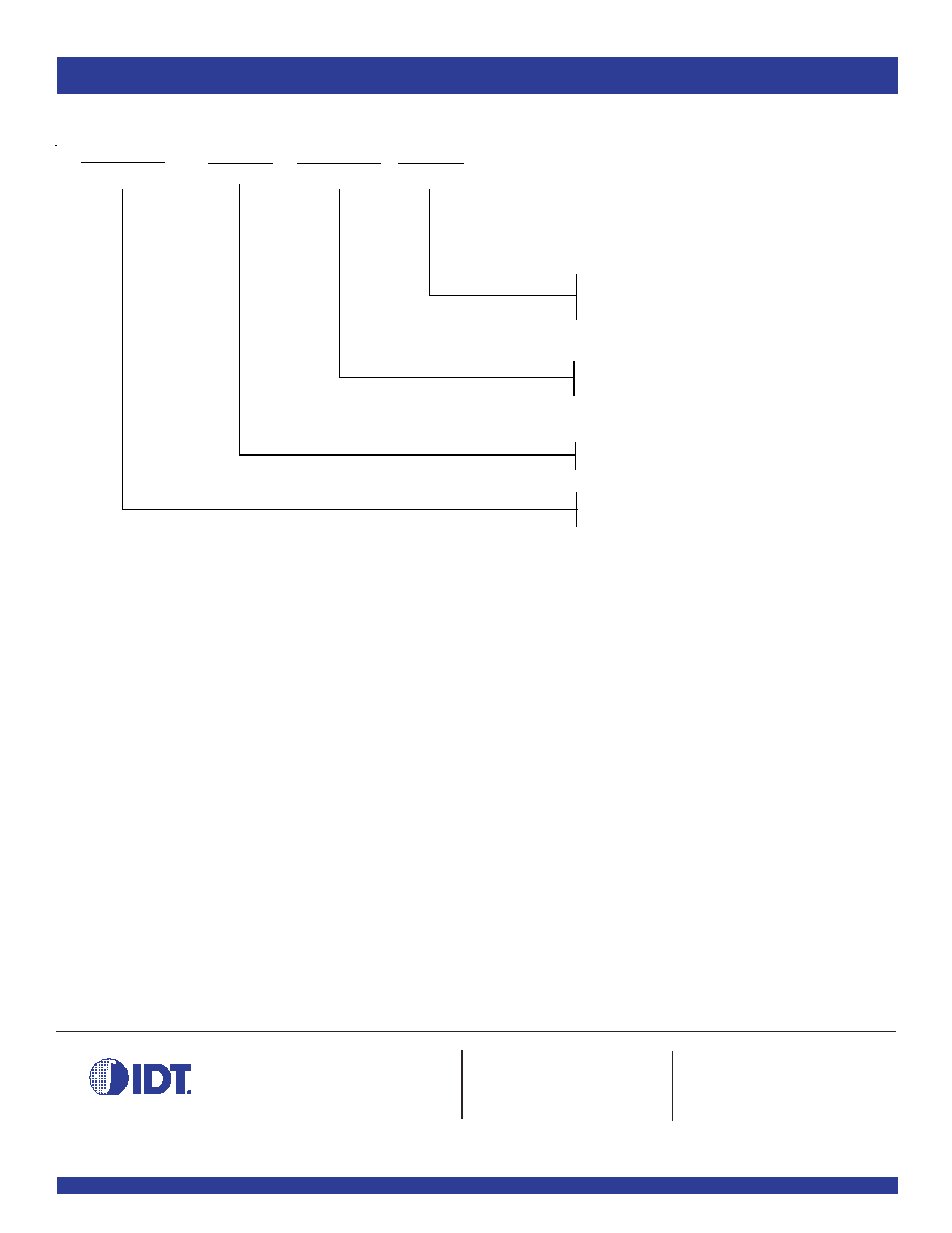
ORDERING INFORMATION
IDT XX
Tem p. Range
XXXX
Device Type
XX
Package
PV
PA
Shrink Sm all Outline Package
Thin Shrink Sm all Outline Package
18-Bit Read/W rite Buffer
74
≠
40
∞
C to +85
∞
C
162
Double-Density, 5 Volt, Balanced Drive
FC T
XXX
Fam ily
701T
701AT
DATA SHEET DOCUMENT HISTORY
1/21/2002
Removed Military temp grade
CORPORATE HEADQUARTERS
for SALES:
for Tech Support:
2975 Stender Way
800-345-7015 or 408-727-6116
logichelp@idt.com
Santa Clara, CA 95054
fax: 408-492-8674
(408) 654-6459
www.idt.com