1
IDT74FCT162952AT/CT/ET
FAST CMOS 16-BIT REGISTERED TRANSCEIVER
INDUSTRIAL TEMPERATURE RANGE
MAY 2002
IDT74FCT162952AT/CT/ET
INDUSTRIAL TEMPERATURE RANGE
FAST CMOS
16-BIT REGISTERED
TRANSCEIVER
DESCRIPTION:
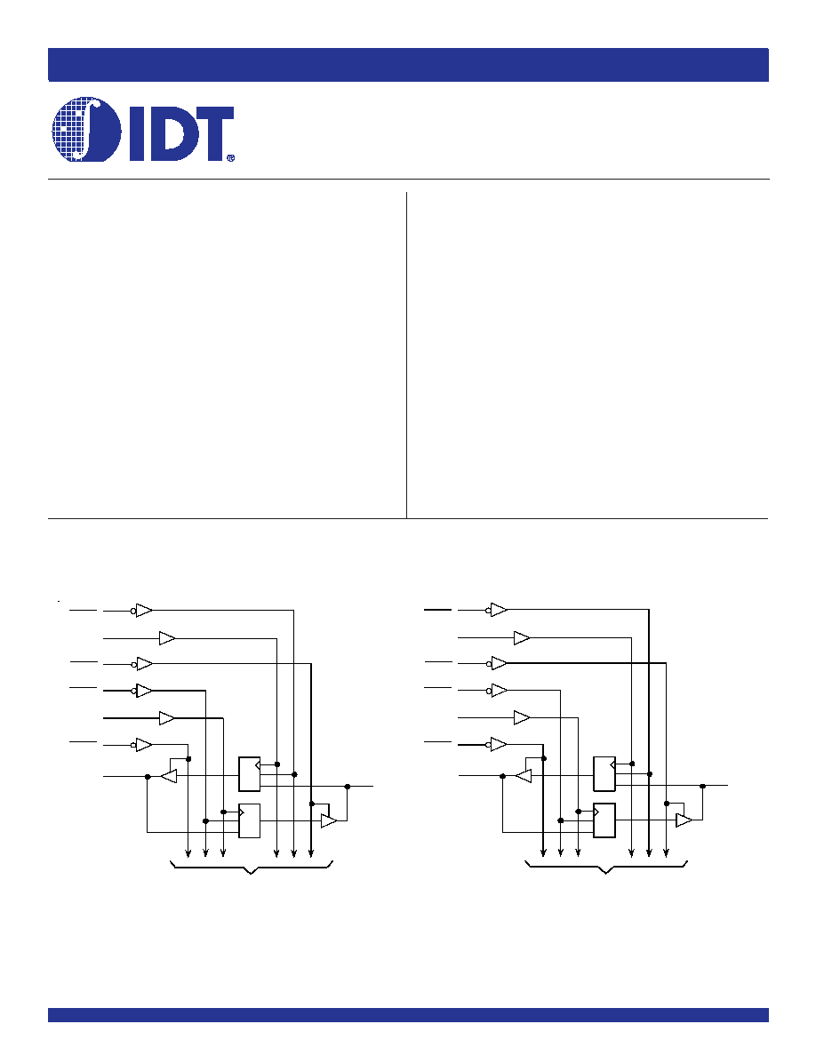
The FCT162952T 16-bit registered transceiver is built using advanced dual
metal CMOS technology. These high-speed, low-power devices are organized
as two independent 8-bit D-type registered transceivers with separate input and
output control for independent control of data flow in either direction. For example,
the A-to-B Enable (xCEAB) must be low to enter data from the A port. xCLKAB
controls the clocking function. When xCLKAB toggles from low-to-high the data
present on the A port will be clocked into the register. xOEAB performs the output
enable function on the B port. Data flow from the B port to A port is similar but
requires using xCEBA, xCLKBA, and xOEBA inputs. Full 16-bit operation is
achieved by tying the control pins of the independent transceivers together.
The FCT162952T have balanced output drive with current limiting resistors.
This offers low ground bounce, minimal undershoot, and controlled output fall
times≠reducing the need for external series terminating resistors. The
FCT162952T is a plug-in replacement for the FCT16952T and ABT16952 for
on-board bus interface applications.
2
O EAB
2
CEBA
2
CLKBA
2
O EBA
2
CEAB
2
CLKAB
2
A
1
2
B
1
TO SEVEN O THE R CH ANN ELS
D
C
D
C
CE
CE
1
O EAB
1
CEBA
1
CLKBA
1
O EBA
1
CEAB
1
CLKAB
1
A
1
1
B
1
TO SEVE N O THER CHANN ELS
D
C
D
C
CE
CE
54
55
1
3
2
56
5
52
31
30
28
26
27
29
15
42
The IDT logo is a registered trademark of Integrated Device Technology, Inc.
© 2002 Integrated Device Technology, Inc.
DSC-5443/3
FEATURES:
∑ 0.5 MICRON CMOS Technology
∑ High-speed, low-power CMOS replacement for ABT functions
∑ Typical t
SK(o)
(Output Skew) < 250ps
∑ Low input and output leakage
1µA (max.)
∑ ESD > 2000V per MIL-STD-883, Method 3015; > 200V using
machine model (C = 200pF, R = 0)
∑ Balanced Output Drivers (±24mA)
∑ Reduced system switching noise
∑ Typical V
OLP
(Output Ground Bounce) < 0.6V at V
CC
= 5V,
T
A
= 25∞C
∑ Power off disable outputs permit "live insertion"
∑ Available in SSOP and TSSOP packages
FUNCTIONAL BLOCK DIAGRAM
2
INDUSTRIAL TEMPERATURE RANGE
IDT74FCT162952AT/CT/ET
FAST CMOS 16-BIT REGISTERED TRANSCEIVER
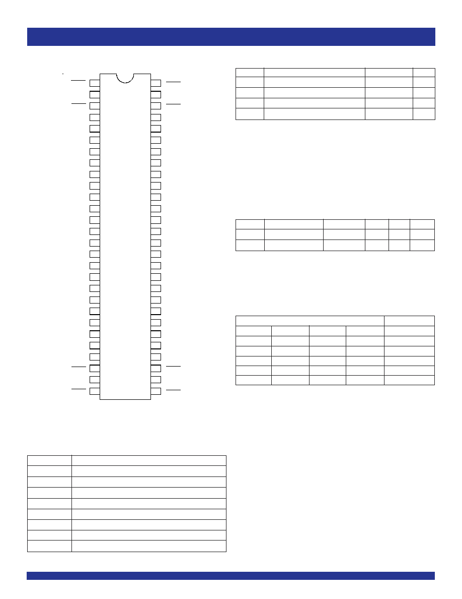
SSOP/ TSSOP
TOP VIEW
PIN CONFIGURATION
1
B
1
1
B
2
GND
1
B
3
1
B
4
V
CC
1
B
5
1
B
6
1
OEBA
1
B
7
1
B
8
2
B
1
2
B
2
GND
2
B
3
2
B
4
V
CC
2
B
5
GND
1
CLKBA
2
B
7
2
B
6
2
B
8
GND
2
CLKBA
2
OEBA
1
CLKAB
GND
1
A
1
1
A
2
V
CC
1
A
3
1
A
4
GND
1
A
5
1
A
6
1
A
7
1
A
8
GND
2
A
1
2
A
2
V
CC
2
A
3
2
A
5
2
A
4
2
A
7
GND
2
A
8
2
CLKAB
2
A
6
1
OEAB
1
CEAB
2
OEAB
2
CEAB
2
CEBA
1
CEBA
47
37
38
39
40
41
42
43
44
45
46
33
34
35
36
56
55
49
50
51
52
53
54
48
1
2
3
4
5
6
7
8
9
10
12
13
14
15
16
17
18
19
20
11
21
22
23
24
29
30
31
32
25
26
27
28
Pin Names
Description
xOEAB
A-to-B Output Enable Input (Active LOW)
xOEBA
B-to-A Output Enable Input (Active LOW)
xCEAB
A-to-B Clock Enable Input (Active LOW)
xCEBA
B-to-A Clock Enable Input (Active LOW)
xCLKAB
A-to-B Clock Input
xCLKBA
B-to-A Clock Input
xAx
A-to-B Data Inputs or B-to-A 3-State Outputs
(1)
xBx
B-to-A Data Inputs or A-to-B 3-State Outputs
(1)
PIN DESCRIPTION
Symbol
Description
Max
Unit
V
TERM
(2)
Terminal Voltage with Respect to GND
≠0.5 to 7
V
V
TERM
(3)
Terminal Voltage with Respect to GND
≠0.5 to V
CC
+0.5
V
T
STG
Storage Temperature
≠65 to +150
∞C
I
OUT
DC Output Current
≠60 to +120
mA
ABSOLUTE MAXIMUM RATINGS
(1)
NOTES:
1. Stresses greater than those listed under ABSOLUTE MAXIMUM RATINGS may cause
permanent damage to the device. This is a stress rating only and functional operation
of the device at these or any other conditions above those indicated in the operational
sections of this specification is not implied. Exposure to absolute maximum rating
conditions for extended periods may affect reliability.
2. All device terminals except FCT162XXX Output and I/O terminals.
3. Output and I/O terminals for FCT162XXX.
Symbol
Parameter
(1)
Conditions
Typ.
Max.
Unit
C
IN
Input Capacitance
V
IN
= 0V
3.5
6
pF
C
OUT
Output Capacitance
V
OUT
= 0V
3.5
8
pF
CAPACITANCE
(T
A
= +25∞C, f = 1.0MHz)
NOTE:
1. This parameter is measured at characterization but not tested.
NOTE:
1. A-to-B data flow is shown: B-to-A data flow is similar but uses xCEBA, xCLKBA,
and xOEBA.
2. Level of B before the indicated steady-state input conditions were established.
3. H = HIGH Voltage Level
L = LOW Voltage Level
X = Don't Care
= LOW-to-HIGH Transition
Z = High-Impedance
Inputs
Outputs
xCEAB
xCLKAB
xOEAB
xAx
xBx
H
X
L
X
B
(2)
X
L
L
X
B
(2)
L
L
L
L
L
L
H
H
X
X
H
X
Z
FUNCTION TABLE
(1, 3)
3
IDT74FCT162952AT/CT/ET
FAST CMOS 16-BIT REGISTERED TRANSCEIVER
INDUSTRIAL TEMPERATURE RANGE
Symbol
Parameter
Test Conditions
(1)
Min.
Typ.
(2)
Max.
Unit
V
IH
Input HIGH Level
Guaranteed Logic HIGH Level
2
--
--
V
V
IL
Input LOW Level
Guaranteed Logic LOW Level
--
--
0.8
V
I
IH
Input HIGH Current (Input pins)
(4)
V
CC
= Max.
V
I
= V
CC
--
--
±1
µA
Input HIGH Current (I/O pins)
(4)
--
--
±1
I
IL
Input LOW Current (Input pins)
(4)
V
I
= GND
--
--
±1
Input LOW Current (I/O pins)
(4)
--
--
±1
I
OZH
High Impedance Output Current
V
CC
= Max.
V
O
= 2.7V
--
--
±1
µA
I
OZL
(3-State Output pins)
(4)
V
O
= 0.5V
--
--
±1
V
IK
Clamp Diode Voltage
V
CC
= Min., I
IN
= ≠18mA
--
≠0.7
≠1.2
V
I
OS
Short Circuit Current
V
CC
= Max., V
O
= GND
(3)
≠80
≠140
≠250
mA
V
H
Input Hysteresis
--
--
100
--
mV
I
CCL
Quiescent Power Supply Current
V
CC
= Max.
--
5
500
µA
I
CCH
V
IN
= GND or V
CC
I
CCZ
DC ELECTRICAL CHARACTERISTICS OVER OPERATING RANGE
Following Conditions Apply Unless Otherwise Specified:
Industrial: T
A
= ≠40∞C to +85∞C, V
CC
= 5.0V ±10%
NOTES:
1. For conditions shown as Min. or Max., use appropriate value specified under Electrical Characteristics for the applicable device type.
2. Typical values are at V
CC
= 5.0V, +25∞C ambient.
3. Not more than one output should be shorted at one time. Duration of the test should not exceed one second.
4. This test limit for this parameter is ±5µA at T
A
= ≠55∞C.
OUTPUT DRIVE CHARACTERISTICS
Symbol
Parameter
Test Conditions
(1)
Min.
Typ.
(2)
Max.
Unit
I
ODL
Output LOW Current
V
CC
= 5V, V
IN
= V
IH
or V
IL
, V
O
= 1.5V
(3)
60
115
200
mA
I
ODH
Output HIGH Current
V
CC
= 5V, V
IN
= V
IH
or V
IL
, V
O
= 1.5V
(3)
≠60
≠115
≠200
mA
V
OH
Output HIGH Voltage
V
CC
= Min.
I
OH
= ≠24mA
2.4
3.3
--
V
V
IN
= V
IH
or V
IL
V
OL
Output LOW Voltage
V
CC
= Min.
I
OL
= 24mA
--
0.3
0.55
V
V
IN
= V
IH
or V
IL

4
INDUSTRIAL TEMPERATURE RANGE
IDT74FCT162952AT/CT/ET
FAST CMOS 16-BIT REGISTERED TRANSCEIVER
Symbol
Parameter
Test Conditions
(1)
Min.
Typ.
(2)
Max.
Unit
I
CC
Quiescent Power Supply
V
CC
= Max.
--
0.5
1.5
mA
Current TTL Inputs HIGH
V
IN
= 3.4V
(3)
I
CCD
Dynamic Power Supply Current
(4)
V
CC
= Max.
V
IN
= V
CC
--
75
120
µA/
Outputs Open
V
IN
= GND
MHz
xOEAB or xOEBA = GND
One Input Toggling
50% Duty Cycle
I
C
Total Power Supply Current
(6)
V
CC
= Max.
V
IN
= V
CC
--
0.8
1.7
mA
Outputs Open
V
IN
= GND
f
CP
= 10MHz (xCLKAB)
50% Duty Cycle
xOEAB = xCEAB = GND
xOEBA = V
CC
V
IN
= 3.4V
--
1.3
3.2
One Bit Toggling
V
IN
= GND
f
i
= 5MHz
50% Duty Cycle
V
CC
= Max.
V
IN
= V
CC
--
3.8
6.5
(5)
Outputs Open
V
IN
= GND
f
CP
= 10MHz (xCLKAB)
50% Duty Cycle
xOEAB = xCEAB = GND
xOEBA = V
CC
V
IN
= 3.4V
--
8.3
20
(5)
Sixteen Bits Toggling
V
IN
= GND
f
i
= 2.5MHz
50% Duty Cycle
NOTES:
1. For conditions shown as Min. or Max., use appropriate value specified under Electrical Characteristics for the applicable device type.
2. Typical values are at V
CC
= 5.0V, +25∞C ambient.
3. Per TTL driven input (V
IN
= 3.4V). All other inputs at V
CC
or GND.
4. This parameter is not directly testable, but is derived for use in Total Power Supply Calculations.
5. Values for these conditions are examples of the I
CC
formula. These limits are guaranteed but not tested.
6. I
C
= I
QUIESCENT
+ I
INPUTS
+ I
DYNAMIC
I
C
= I
CC
+
I
CC
D
H
N
T
+ I
CCD
(f
CP
N
CP
/2 + fiNi)
I
CC
= Quiescent Current (I
CCL
, I
CCH
and I
CCZ
)
I
CC
= Power Supply Current for a TTL High Input (V
IN
= 3.4V)
D
H
= Duty Cycle for TTL Inputs High
N
T
= Number of TTL Inputs at D
H
I
CCD
= Dynamic Current Caused by an Input Transition Pair (HLH or LHL)
f
CP
= Clock Frequency for Register Devices (Zero for Non-Register Devices)
N
CP
= Number of Clock Inputs at f
CP
f
i
= Input Frequency
N
i
= Number of Inputs at f
i
POWER SUPPLY CHARACTERISTICS

5
IDT74FCT162952AT/CT/ET
FAST CMOS 16-BIT REGISTERED TRANSCEIVER
INDUSTRIAL TEMPERATURE RANGE
FCT162952AT
FCT162952CT
FCT162952ET
Symbol
Parameter
Condition
(1)
Min.
(2)
Max.
Min.
(2)
Max.
Min.
(2)
Max.
Unit
t
PLH
Propagation Delay
C
L
= 50pF
2
10
2
6.3
1.5
3.7
ns
t
PHL
xCLKAB, xCLKBA to xBx, xAx
R
L
= 500
t
PZH
Output Enable Time
1.5
10.5
1.5
7
1.5
4.4
ns
t
PZL
xOEBA, xOEAB to xAx, xBx
t
PHZ
Output Disable Time
1.5
10
1.5
6.5
1.5
3.6
ns
t
PLZ
xOEBA, xOEAB to xAx, xBx
t
SU
Set-up Time, HIGH or LOW
2.5
--
2.5
--
1.5
--
ns
xAx, xBx to xCLKAB, xCLKBA
t
H
Hold Time HIGH or LOW
2
--
1.5
--
0
--
ns
xAx, xBx to xCLKAB, xCLKBA
t
SU
Set-up Time, HIGH or LOW
3
--
3
--
2
--
ns
xCEAB, xCEBA to xCLKAB, xCLKBA
t
H
Hold Time HIGH or LOW
2
--
2
--
0
--
ns
xCEAB, xCEBA to xCLKAB, xCLKBA
t
W
Pulse Width HIGH or LOW
3
--
3
--
3
--
ns
xCLKAB or xCLKBA
(3)
t
SK(o)
Output Skew
(4)
--
0.5
--
0.5
--
0.5
ns
SWITCHING CHARACTERISTICS OVER OPERATING RANGE
NOTES:
1. See test circuit and waveforms.
2. Minimum limits are guaranteed but not tested on Propagation Delays.
3. Guaranteed but not tested
4. Skew between any two outputs of the same package switching in the same direction. This parameter is guaranteed by design.
6
INDUSTRIAL TEMPERATURE RANGE
IDT74FCT162952AT/CT/ET
FAST CMOS 16-BIT REGISTERED TRANSCEIVER
Pulse
G enerator
R
T
D .U.T.
V
C C
V
IN
C
L
V
O UT
50pF
500
500
7.0V
3V
1.5V
0V
3V
1.5V
0V
3V
1.5V
0V
3V
1.5V
0V
DATA
INPUT
TIMING
INPUT
ASYNCH RO NO US C O NTRO L
PRESET
C LEAR
ETC.
SYN CHRO N OU S C ON TR OL
t
SU
t
H
t
R EM
t
SU
t
H
PRESET
C LEAR
CLO CK ENABL E
ETC.
HIG H-LO W -HIG H
PULS E
LO W -H IG H-LOW
PULS E
t
W
1.5V
1.5V
SAME PHASE
INPUT TRAN SITIO N
3V
1.5V
0V
1.5V
V
O H
t
PLH
OUTPUT
O PPO SITE P HASE
INPUT TRAN SITIO N
3V
1.5V
0V
t
PLH
t
PH L
t
PH L
V
O L
CON TRO L
INPUT
3V
1.5V
0V
3.5V
0V
O UTPUT
NO RMALLY
LO W
O UTPUT
NO RMALLY
H IG H
SW ITCH
CLO SE D
SW ITCH
O PEN
V
O L
0.3V
0.3V
t
PLZ
t
PZL
t
PZH
t
PH Z
3.5V
0V
1.5V
1.5V
ENABLE
DISABLE
V
OH
Test
Switch
Open Drain
Disable Low
Closed
Enable Low
All Other Tests
Open
SWITCH POSITION
DEFINITIONS:
C
L
= Load capacitance: includes jig and probe capacitance.
R
T
= Termination resistance: should be equal to Z
OUT
of the Pulse Generator.
Test Circuits for All Outputs
Set-up, Hold, and Release Times
Propagation Delay
Enable and Disable Times
NOTES:
1. Diagram shown for input Control Enable-LOW and input Control Disable-HIGH.
2. Pulse Generator for All Pulses: Rate
1.0MHz; t
F
2.5ns; t
R
2.5ns.
Pulse Width
TEST CIRCUITS AND WAVEFORMS
7
IDT74FCT162952AT/CT/ET
FAST CMOS 16-BIT REGISTERED TRANSCEIVER
INDUSTRIAL TEMPERATURE RANGE
ORDERING INFORMATION
CORPORATE HEADQUARTERS
for SALES:
for Tech Support:
2975 Stender Way
800-345-7015 or 408-727-6116
logichelp@idt.com
Santa Clara, CA 95054
fax: 408-492-8674
(408) 654-6459
www.idt.com
DATA SHEET DOCUMENT HISTORY
1/21/2002
Removed Military temp grade
4/10/2002
Removed B speed grade
5/21/2002
Removed TVSOP package
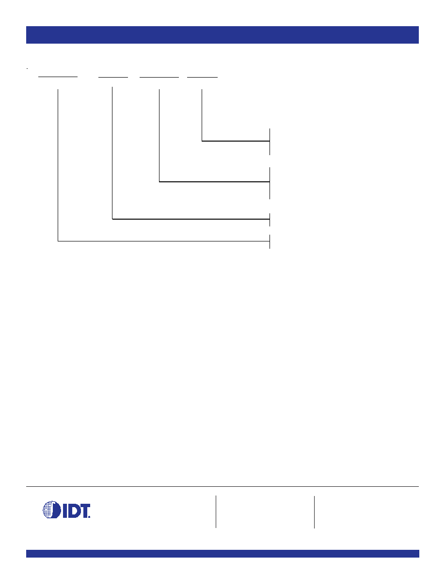
IDT XX
Temp. Range
XXXX
Device Type
XX
Package
PV
PA
Shrink Small Outline Package
Thin Shrink Small Outline Package
16-Bit Registered Transceiver
74
≠
40
∞
C to +85
∞
C
162
Double-Density, 5 Volt, Balanced Drive
FCT
XXX
Family
952AT
952CT
952ET