Integrated Device Technology, Inc.
MILITARY AND COMMERCIAL TEMPERATURE RANGES
AUGUST 1996
©
1996 Integrated Device Technology, Inc.
5.5
DSC-3071/3
IDT54/74FCT162H272AT/CT/ET
1
The IDT logo is a registered trademark of Integrated Device Technology, Inc.
FAST CMOS
12-BIT SYNCHRONOUS
BUS EXCHANGER
FEATURES:
∑ 0.5 MICRON CMOS Technology
∑ Typical t
SK
(o) (Output Skew) < 250ps
∑ Low input and output leakage
1
µ
A (max.)
∑ ESD > 2000V per MIL-STD-883, Method 3015;
> 200V using machine model (C = 200pF, R = 0)
∑ Packages include 25 mil pitch SSOP, 19.6 mil pitch TSSOP,
15.7 mil pitch TVSOP and 25 mil pitch Cerpack
∑ Extended commercial range of -40
∞
C to +85
∞
C
∑ Balanced Output Drivers:
±
24mA (commercial)
±
16mA (military)
∑ Reduced system switching noise
∑ Typical V
OLP
(Output Ground Bounce) < 0.6V at
V
CC
= 5V, T
A
= 25
∞
C
∑ Bus Hold retains last active bus state during 3-state
∑ Eliminates the need for external pull up resistors
multiplexers for use in synchronous memory interleaving
applications. All registers have a common clock and use a
clock enable (
CE
xxx) on each data register to control data
sequencing. The output enables and mux select (
OEA
,
OEB
and SEL) are also under synchronous control allowing direc-
tion changes to be edge triggered events.
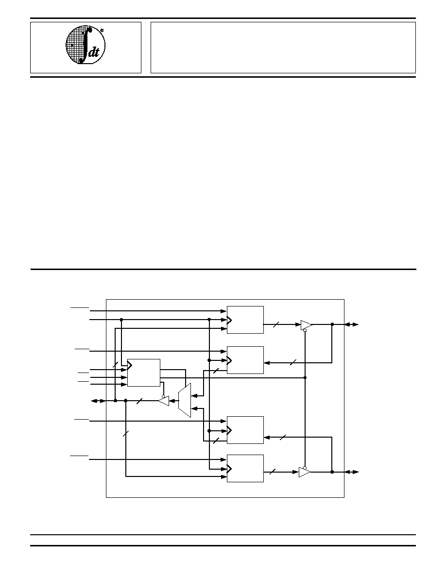
The tri-port bus exchanger has three 12-bit ports. Data may
be transferred between the A port and either/both of the B
ports. The clock enable (
CE1B
,
CE2B
,
CEA1B
and
CEA2B
)
inputs control the data storage. Both B ports have a common
output enable (
OEB
) to aid in synchronously loading the B
registers from the B port.
The FCT162H272AT/CT/ET have balanced output drive
with current limiting resistors. This offers low ground bounce,
minimal undershoot, and controlled output fall times-reducing
the need for external series terminating resistors.
The FCT162H272AT/CT/ET have "Bus Hold" which re-
tains the input's last state whenever the input goes to high
impedance. This prevents "floating" inputs and eliminates the
need for pull-up/down resistors.
DESCRIPTION:
The FCT162H272AT/CT/ET synchronous tri-port bus ex-
changers are high-speed, bidirectional,12-bit, registered, bus
FUNCTIONAL BLOCK DIAGRAM
A-1B
REGISTER
CLK
SEL
12
M
U
X
12
12
A
1:12
1B
1:12
12
12
12
12
12
2B
1:12
CE1B
CEA1B
1
0
OEB
OEA
CE2B
CEA2B
1B-A
REGISTER
12
2B-A
REGISTER
A-2B
REGISTER
CONTROL
REGISTER
CE
D
Q
CE
D
Q
CE
D
Q
CE
D
Q
3071 drw 01

5.5
2
IDT54/74FCT162H272AT/CT/ET
FAST CMOS 12-BIT SYNCHRONOUS TRI-PORT BUS EXCHANGER
MILITARY AND COMMERCIAL TEMPERATURES RANGES
PIN CONFIGURATIONS
3071 drw 03
3071 drw 02
CE1B
2B
5
2B
6
GND
2B
7
2B
8
V
CC
2B
9
2B
10
2B
4
2B
11
2B
12
1B
12
1B
11
GND
1B
10
1B
9
V
CC
1B
8
GND
CE2B
1B
6
1B
7
1B
5
GND
1B
4
CLK
OEB
CEA1B
CEA2B
2B
3
GND
2B
2
2B
1
V
CC
A
1
A
2
GND
A
3
A
4
A
5
A
6
GND
A
7
A
8
V
CC
A
9
1B
3
A
11
A
10
1B
1
GND
1B
2
SEL
A
12
OEA
47
37
38
39
40
41
42
43
44
45
46
33
34
35
36
56
55
49
50
51
52
53
54
48
1
2
3
4
5
6
7
8
9
10
12
13
14
15
16
17
18
19
20
11
21
22
23
24
29
30
31
32
25
26
27
28
CERPACK
TOP VIEW
E56-1
CEA1B
CEA2B
GND
2B
2
V
CC
A
3
A
6
A
7
GND
A
12
2B
3
2B
1
A
1
A
2
GND
A
4
A
5
A
8
A
9
A
10
V
CC
1B
1
A
11
1B
2
CE2B
2B
4
GND
2B
5
2B
6
V
CC
2B
7
2B
8
GND
2B
10
2B
11
2B
12
1B
11
1B
10
GND
1B
9
V
CC
1B
6
1B
8
2B
9
1B
12
1B
7
1B
5
CE1B
39
29
30
31
32
33
34
35
36
37
38
25
26
27
28
48
47
41
42
43
44
45
46
40
1
2
3
4
5
6
7
8
9
10
12
13
14
15
16
17
18
19
20
11
21
22
23
24
SSOP/
TSSOP/TVSOP
TOP VIEW
SO56-1
SO56-2
SO56-3
OEA
GND
SEL
1B
3
CLK
GND
1B
4
OEB
49
56
55
50
51
52
53
54
5.5
3
IDT54/74FCT162H272AT/CT/ET
FAST CMOS 12-BIT SYNCHRONOUS TRI-PORT BUS EXCHANGER
MILITARY AND COMMERCIAL TEMPERATURES RANGES
NOTES:
1. Output level before the indicated steady-state input conditions were
established.
2. H = HIGH Voltage Level
L = LOW Voltage Level
X = Don't Care
Z = High Impedance
= LOW-to-HIGH Transition
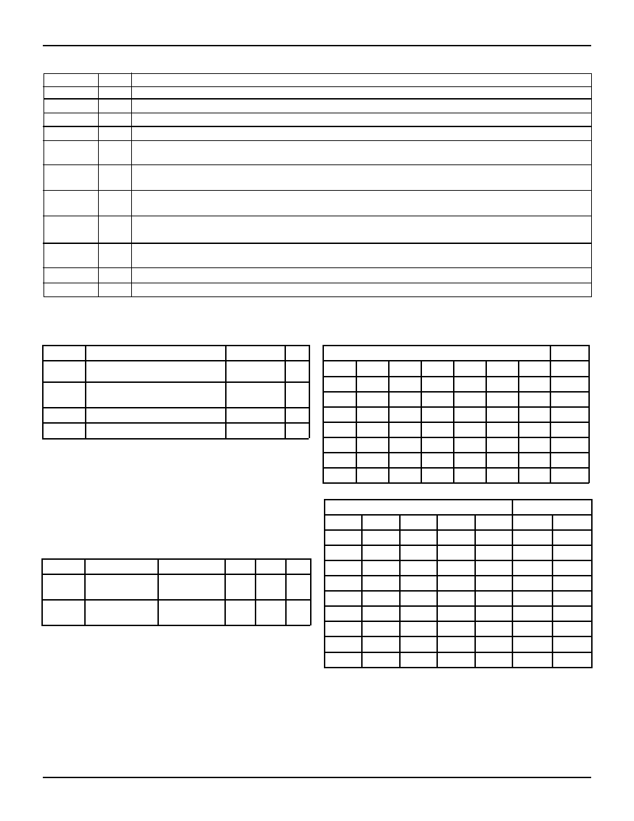
ABSOLUTE MAXIMUM RATINGS
(1)
FUNCTION TABLES
(2)
3071 tbl 04
3071 tbl 05
NOTES:
1. On FCT162H272T these pins have "Bus Hold". All other pins are standard inputs, outputs or I/Os.
PIN DESCRIPTION
Signal
I/O
Description
A
(1:12)
I/O
Bidirectional Data Port A. Usually connected to the CPU's Address/Data bus.
(1)
1B
(1:12)
I/O
Bidirectional Data Port 1B. Usually connected to the even path or even bank of memory.
(1)
2B
(1:12
)
I/O
Bidirectional Data Port 2B. Usually connected to the odd path or odd bank of memory.
(1)
CLK
I
Clock Input.
CEA1B
I
Clock Enable Input for the A-1B Register. If
CEA1B
is LOW during the rising edge of CLK, data will be clocked
into register A-1B (Active LOW).
CEA2B
I
Clock Enable Input for the A-2B Register. If
CEA2B
is LOW during the rising edge of CLK, data will be clocked
into register A-2B (Active LOW).
CE1B
I
Clock Enable Input for the 1B-A Register. If
CE1B
is LOW during the rising edge of CLK, data will be clocked into
register 1B-A (Active LOW).
CE2B
I
Clock Enable Input for the 2B-A Register. If
CE2B
is LOW during the rising edge of CLK, data will be clocked into
register 2B-A (Active LOW).
SEL
I
1B or 2B Path Selection. When HIGH during the rising edge of CLK, SEL enables data transfer from 1B Port to
A Port. When LOW during the rising edge of CLK, SEL enables data transfer from 2B Port to A Port.
OEA
I
Synchronous Output Enable for A Port (Active LOW).
OEB
I
Synchronous Output Enable for 1B Port and 2B Port (Active LOW).
3071 tbl 01
Inputs
Output
1B
2B
SEL
CE1B
CE1B CE2B
CE2B OEA
OEA
CLK
A
H
X
H
L
X
L
H
L
X
H
L
X
L
L
X
X
H
H
X
L
A
(1)
X
H
L
X
L
L
H
X
L
L
X
L
L
L
X
X
L
X
H
L
A
(1)
X
X
X
X
X
H
Z
Inputs
Outputs
A
CEA1B
CEA1B CEA2B
CEA2B
OEB
OEB
CLK
1B
2B
H
L
L
L
H
H
L
L
L
L
L
L
H
L
H
L
H
B
(1)
L
L
H
L
L
B
(1)
H
H
L
L
B
(1)
H
L
H
L
L
B
(1)
L
X
H
H
L
B
(1)
B
(1)
X
X
X
H
Z
Z
X
X
X
L
Active
Active
Symbol
Description
Max.
Unit
V
TERM(2)
Terminal Voltage with Respect to
GND
≠0.5 to +7.0
V
V
TERM(3)
Terminal Voltage with Respect to
GND
≠0.5 to
V
CC
+0.5
V
T
STG
Storage Temperature
≠65 to +150
∞
C
I
OUT
DC Output Current
≠60 to +120 mA
NOTES:
1. Stresses greater than those listed under ABSOLUTE MAXIMUM RAT-
INGS may cause permanent damage to the device. This is a stress rating
only and functional operation of the device at these or any other condi-
tions above those indicated in the operational sections of this specifica-
tion is not implied. Exposure to absolute maximum rating conditions for
extended periods may affect reliability.
2. All device terminals except FCT162XXXT Output and I/O terminals.
3. Output and I/O terminals for FCT162XXXT.
3071 tbl 02
NOTE:
1. This parameter is measured at characterization but not tested.
CAPACITANCE
(T
A
= +25
∞
C, F = 1.0MH
Z
)
3071 tbl 03
Symbol
Parameter
(1)
Conditions
Typ.
Max.
Unit
C
IN
Input
Capacitance
V
IN
= 0V
3.5
6.0
pF
C
I/O
I/O
Capacitance
V
OUT
= 0V
3.5
8.0
pF

5.5
4
IDT54/74FCT162H272AT/CT/ET
FAST CMOS 12-BIT SYNCHRONOUS TRI-PORT BUS EXCHANGER
MILITARY AND COMMERCIAL TEMPERATURES RANGES
DC ELECTRICAL CHARACTERISTICS OVER OPERATING RANGE (BUS HOLD)
Following Conditions Apply Unless Otherwise Specified:
Commercial: T
A
= ≠40
∞
C to +85
∞
C, V
CC
= 5.0V
±
10%; Military: T
A
= ≠55
∞
C to +125
∞
C, V
CC
= 5.0V
±
10%
NOTES:
1. For conditions shown as Max. or Min., use appropriate value specified under Electrical Characteristics for the applicable device type.
2. Typical values are at Vcc = 5.0V, +25
∞
C ambient.
3. Not more than one output should be tested at one time. Duration of the test should not exceed one second.
4. Pins with Bus Hold are identified in the pin description.
5. The test limit for this parameter is
±
5
µ
A at T
A
= ≠55
∞
C.
6. Does not include Bus Hold I/O pins.
OUTPUT DRIVE CHARACTERISTICS FOR FCT162H272T
3071 lnk 08
Symbol
Parameter
Test Conditions
(1)
Min.
Typ.
(2)
Max.
Unit
I
ODL
Output LOW Current
V
CC
= 5V, V
IN
= V
IH
or
V
IL,
V
OUT
= 1.5V
(3)
60
115
200
mA
I
ODH
Output HIGH Current
V
CC
= 5V, V
IN
= V
IH
or V
IL,
V
OUT
= 1.5V
(3)
≠60
≠115
≠200
mA
V
OH
Output HIGH Voltage
V
CC
= Min.
V
IN
= V
IH
or V
IL
I
OH
= ≠16mA MIL.
I
OH
= ≠24mA COM'L.
2.4
3.3
--
V
V
OL
Output LOW Voltage
V
CC
= Min.
V
IN
= V
IH
or V
IL
I
OL
= 16mA MIL.
I
OL
= 24mA COM'L.
--
0.3
0.55
V
Symbol
Parameter
Test Conditions
(1)
Min.
Typ.
(2)
Max.
Unit
V
IH
Input HIGH Level
Guaranteed Logic HIGH Level
2.0
--
--
V
V
IL
Input LOW Level
Guaranteed Logic LOW Level
--
--
0.8
V
I
I H
Input
Standard Input
(5)
V
CC
= Max.
V
I
= V
CC
--
--
±
1
µ
A
HIGH
Standard I/O
(5)
--
--
±
1
Current
(4)
Bus-Hold Input
--
--
±
100
Bus-Hold I/O
--
--
±
100
I
I L
Input
Standard Input
(5)
V
I
= GND
--
--
±
1
LOW
Standard I/O
(5)
--
--
±
1
Current
(4)
Bus-Hold Input
--
--
±
100
Bus-Hold I/O
--
--
±
100
I
BHH
Bus Hold
Bus-Hold Input
V
CC
= Min.
V
I
= 2.0V
≠50
--
--
µ
A
I
BHL
Sustain
Current
(4)
V
I
= 0.8V
+50
--
--
I
OZH
High Impedance Output Current
V
CC
= Max.
V
O
= 2.7V
--
--
±
1
µ
A
I
OZL
(3-State Output pins)
(5,6)
V
O
= 0.5V
--
--
±
1
V
IK
Clamp Diode Voltage
V
CC
= Min., I
IN
= ≠18mA
--
≠
0.7
≠
1.2
V
I
OS
Short Circuit Current
V
CC
= Max., V
O
= GND
(3)
≠80
≠
140
≠
225
mA
V
H
Input Hysteresis
--
--
100
--
mV
I
CCL
I
CCH
I
CCZ
Quiescent Power Supply Current
V
CC
= Max., V
IN
= GND or V
CC
--
5
500
µ
A
3071 tbl 06

5.5
5
IDT54/74FCT162H272AT/CT/ET
FAST CMOS 12-BIT SYNCHRONOUS TRI-PORT BUS EXCHANGER
MILITARY AND COMMERCIAL TEMPERATURES RANGES
NOTES:
1. For conditions shown as Max. or Min., use appropriate value specified under Electrical Characteristics for the applicable device type.
2. Typical values are at V
CC
= 5.0V, +25
∞
C ambient.
3. Per TTL driven input (V
IN
= 3.4V). All other inputs at V
CC
or GND.
4. This parameter is not directly testable, but is derived for use in Total Power Supply Calculations.
5. Values for these conditions are examples of the I
CC
formula. These limits are guaranteed but not tested.
6. I
C
= I
QUIESCENT
+ I
INPUTS
+ I
DYNAMIC
I
C
= I
CC
+
I
CC
D
H
N
T
+ I
CCD
(f
CP
N
CP
/2 + f
i
N
i
)
I
CC
= Quiescent Current (I
CCL
,
I
CCH
and I
CCZ
)
I
CC
= Power Supply Current for a TTL High Input (V
IN
= 3.4V)
D
H
= Duty Cycle for TTL Inputs High
N
T
= Number of TTL Inputs at D
H
I
CCD
= Dynamic Current Caused by an Input Transition Pair (HLH or LHL)
f
CP
= Clock Frequency for Register Devices (Zero for Non-Register Devices)
N
CP
= Number of Clock Inputs at f
CP
f
i
= Input Frequency
N
i
= Number of Inputs at f
i
POWER SUPPLY CHARACTERISTICS
3071 tbl 09
Symbol
Parameter
Test Conditions
(1)
Min.
Typ.
(2)
Max.
Unit
I
CC
Quiescent Power Supply Current
TTL Inputs HIGH
V
CC
= Max.
V
IN
= 3.4V
(3)
--
0.5
1.5
mA
I
CCD
Dynamic Power Supply Current
(4)
V
CC
= Max.
Outputs Open
One Output Port Enabled
CExx
= GND
One Input Bit Toggling
One Output Bit Toggling
50% Duty Cycle
V
IN
= V
CC
V
IN
= GND
--
60
100
µ
A/
MHz
I
C
Total Power Supply Current
(6)
V
CC
= Max.
Outputs Open
fi = 10MHz
V
IN
= V
CC
V
IN
= GND
--
0.6
1.5
mA
50% Duty Cycle
One Output Port Enabled
CExx
= GND
One Input Bit Toggling
One Output Bit Toggling
V
IN
= 3.4V
V
IN
= GND
--
0.9
2.3
V
CC
= Max.
Outputs Open
fi = 2.5MHz
V
IN
= V
CC
V
IN
= GND
--
1.8
3.5
(5)
50% Duty Cycle
One Output Port Enabled
CExx
= GND
Twelve Input Bits Toggling
Twelve Output Bits Toggling
V
IN
= 3.4V
V
IN
= GND
--
4.8
12.5
(5)