162h952
1
IDT54/74FCT162H952AT/BT/CT/ET
FAST CMOS 16-BIT REGISTERED TRANSCEIVER
MILITARY AND COMMERCIAL TEMPERATURE RANGES
AUGUST 1999
1999 Integrated Device Technology, Inc.
DSC-5441/-
c
IDT54/74FCT162H952AT/BT/CT/ET
MILITARY AND COMMERCIAL TEMPERATURE RANGES
FAST CMOS
16-BIT REGISTERED
TRANSCEIVER
DESCRIPTION:
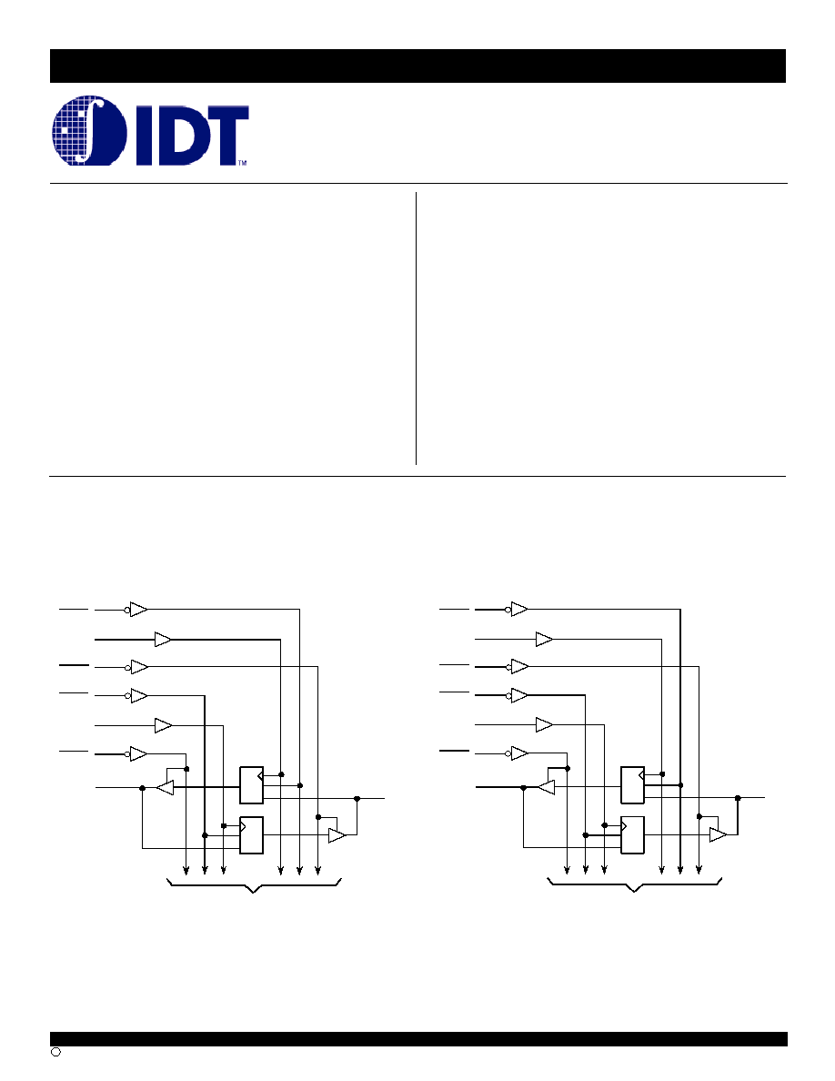
The FCT162H952AT/BT/CT/ET 16-bit registered transceiver is built
using advanced dual metal CMOS technology. These high-speed, low-
power devices are organized as two independent 8-bit D-type registered
transceivers with separate input and output control for independent control
of data flow in either direction. For example, the A-to-B Enable (x
CEAB)
must be LOW to enter data from the A port. xCLKAB controls the clocking
function. When xCLKAB toggles from LOW-to-HIGH, the data present on the
A port will be clocked into the register. x
OEAB performs the output enable
function on the B port. Data flow from the B port to A port is similar but requires
using x
CEBA, xCLKBA, and xOEBA inputs. Full 16-bit operation is
achieved by tying the control pins of the independent transceivers together.
The FCT162H952AT/BT/CT/ET has "Bus Hold" which retains the
input's last state whenever the input goes to high impedance. This prevents
"floating" inputs and eliminates the need for pull-up/down resistors.
FUNCTIONAL BLOCK DIAGRAM
2
OEAB
2
CE BA
2
CLKBA
2
OEBA
2
CE AB
2
CLKAB
2
A
1
2
B
1
TO SEVEN OTHER CHANNELS
D
C
D
C
C E
C E
1
OEAB
1
CE BA
1
CLKBA
1
OEBA
1
CE AB
1
CLKAB
1
A
1
1
B
1
TO SEVEN OTHER CHANN ELS
D
C
D
C
C E
C E
54
55
1
3
2
56
5
52
31
30
28
26
27
29
15
42
FEATURES:
-
0.5 MICRON CMOS Technology
-
High-speed, low-power CMOS replacement for ABT functions
-
Typical t
SK
(o) (Output Skew) < 250ps
-
Low input and output leakage
1� A (max.)
-
ESD > 2000V per MIL-STD-883, Method 3015; > 200V using
machine model (C = 200pF, R = 0)
-
25 mil pitch SSOP, 19.6 mil pitch TSSOP, 15.7 mil pitch TVSOP
and 25 mil pitch CERPACK packages
-
Extended commercial range of -40�C to +85�C
-
Bus Hold retains last active bus state during 3-state
-
Eliminates the need for external pull up resistors
2
MILITARY AND COMMERCIAL TEMPERATURE RANGES
IDT54/74FCT162H952AT/BT/CT/ET
FAST CMOS 16-BIT REGISTERED TRANSCEIVER
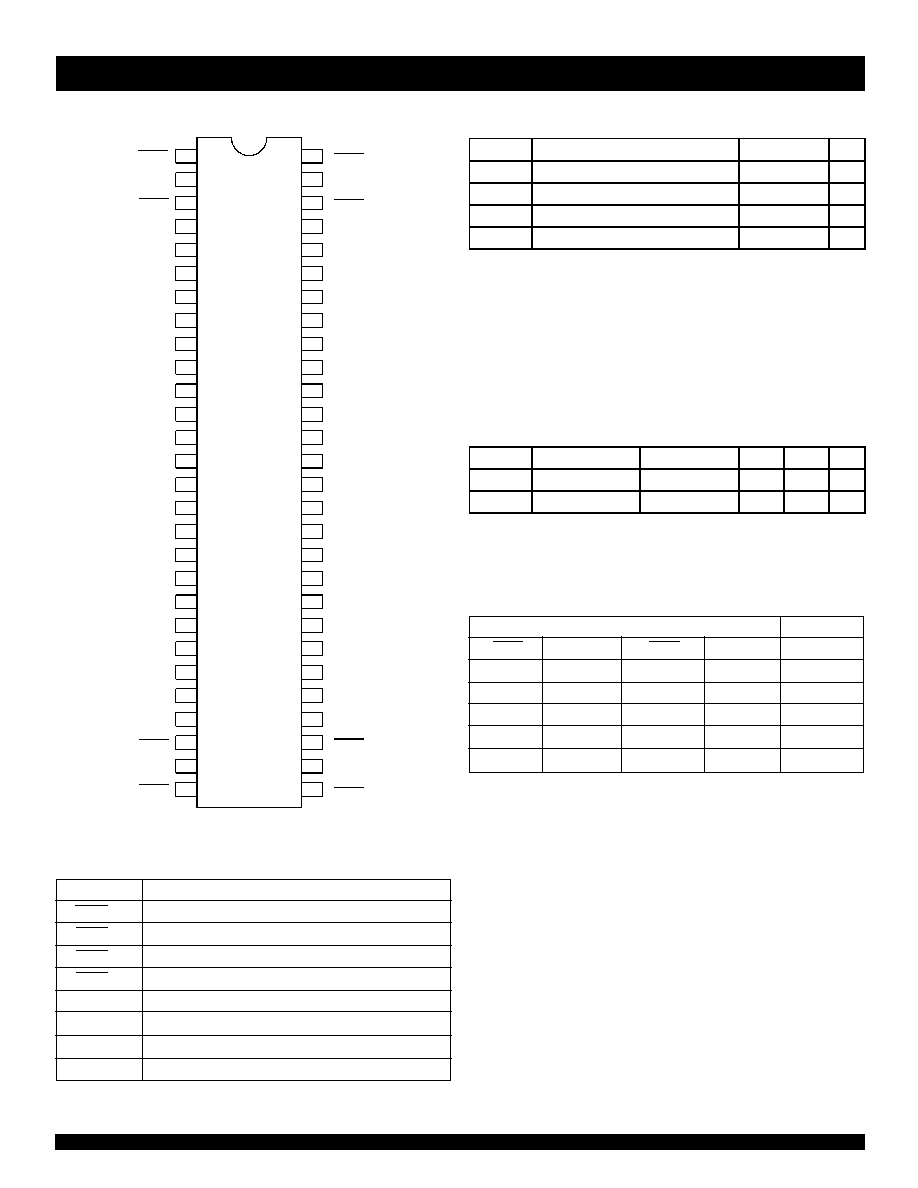
SSOP/ TSSOP/ TVSOP/ CERPACK
TOP VIEW
PIN CONFIGURATION
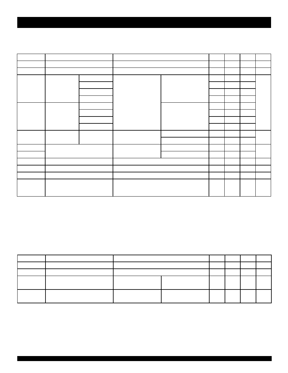
ABSOLUTE MAXIMUM RATINGS
(1)
Symbol
Description
Max
Unit
V
TERM(2)
Terminal Voltage with Respect to GND
�0.5 to +7
V
V
TERM(3)
Terminal Voltage with Respect to GND
�0.5 to V
CC
+0.5
V
T
STG
Storage Temperature
�65 to +150
�C
I
OUT
DC Output Current
�60 to +120
mA
5v16-link
NOTES:
1. Stresses greater than those listed under ABSOLUTE MAXIMUM
RATINGS may cause permanent damage to the device. This is a
stress rating only and functional operation of the device at these or
any other conditions above those indicated in the operational sections
of this specification is not implied. Exposure to absolute maximum
rating conditions for extended periods may affect reliability.
2. All device
terminals except FCT162XXXT Output and I/O terminals.
3. Output and I/O terminals for FCT162XXXT.
CAPACITANCE (T
A
= +25
O
C, f = 1.0MHz)
Symbol
Parameter
(1)
Conditions
Typ.
Max.
Unit
C
IN
Input Capacitance
V
IN
= 0V
3.5
6
pF
C
OUT
Output Capacitance
V
OUT
= 0V
3.5
8
pF
5v16-link
NOTE:
1. This parameter is measured at characterization but not tested.
1
B
1
1
B
2
G ND
1
B
3
1
B
4
V
CC
1
B
5
1
B
6
1
O EBA
1
B
7
1
B
8
2
B
1
2
B
2
G ND
2
B
3
2
B
4
V
CC
2
B
5
G ND
1
C LKBA
2
B
7
2
B
6
2
B
8
G ND
2
C LKBA
2
O EBA
1
C LK AB
G ND
1
A
1
1
A
2
V
CC
1
A
3
1
A
4
G ND
1
A
5
1
A
6
1
A
7
1
A
8
G ND
2
A
1
2
A
2
V
CC
2
A
3
2
A
5
2
A
4
2
A
7
G ND
2
A
8
2
C LK AB
2
A
6
1
O EAB
1
C EAB
2
O EAB
2
C EAB
2
C EBA
1
C EBA
47
37
38
39
40
41
42
43
44
45
46
33
34
35
36
56
55
49
50
51
52
53
54
48
1
2
3
4
5
6
7
8
9
10
12
13
14
15
16
17
18
19
20
11
21
22
23
24
SO 56-1
SO 56-2
SO 56-3
E56-1
29
30
31
32
25
26
27
28
FUNCTION TABLE
(1,3)
Inputs
Outputs
xCEAB
xCLKAB
xOEAB
xAx
xBx
H
X
L
X
B
(2)
X
L
L
X
B
(2)
L
L
L
L
L
L
H
H
X
X
H
X
Z
NOTES:
1. A-to-B data flow is shown: B-to-A data flow is similar but uses x
CEBA
,
xCLKBA, and x
OEBA
.
2. Level of B before the indicated steady-state input conditions were
established.
3. H = HIGH Voltage Level
L = LOW Voltage Level
X = Don't Care
= LOW-to-HIGH Transition
Z = High-impedance
PIN DESCRIPTION
Pin Names
Description
xOEAB
A-to-B Output Enable Input (Active LOW)
xOEBA
B-to-A Output Enable Input (Active LOW)
xCEAB
A-to-B Clock Enable Input (Active LOW)
xCEBA
B-to-A Clock Enable Input (Active LOW)
xCLKAB
A-to-B Clock Input
xCLKBA
B-to-A Clock Input
x A x
A-to-B Data Inputs or B-to-A 3-State Outputs
(1)
x B x
B-to-A Data Inputs or A-to-B 3-State Outputs
(1)
NOTE:
1. These pins have "Bus Hold". All other pins are standard inputs, outputs
or I/Os.
3
IDT54/74FCT162H952AT/BT/CT/ET
FAST CMOS 16-BIT REGISTERED TRANSCEIVER
MILITARY AND COMMERCIAL TEMPERATURE RANGES
NOTES:
1. For conditions shown as Max. or Min., use appropriate value specified under Electrical Characteristics for the applicable device type.
2. Typical values are at Vcc = 5.0V, +25�C ambient.
3. Not more than one output should be tested at one time. Duration of the test should not exceed one second.
4. Pins with Bus-hold are identified in the pin description.
5. The test limit for this parameter is � 5�A at T
A
= �55�C.
6. Does not include Bus-hold I/O pins.
DC ELECTRICAL CHARACTERISTICS OVER OPERATING RANGE (BUS-HOLD)
Following Conditions Apply Unless Otherwise Specified:
Commercial: T
A
= -40�C to +85�C, V
CC
= 5.0
V
�10%; Military: T
A
= -55�C to +125�C, V
CC
= 5.0
V
�10%
Symbol
Parameter
Test Conditions
(1)
Min.
Typ.
(2)
Max.
Unit
V
IH
Input HIGH Level
Guaranteed Logic HIGH Level
2
--
--
V
V
IL
Input LOW Level
Guaranteed Logic LOW Level
--
--
0.8
V
I
IH
Input
Standard Input
(5)
V
CC
= Max.
V
I
= V
CC
--
--
�
1
� A
HIGH
Standard I/O
(5)
--
--
�
1
Current
(4)
Bus-hold Input
--
--
�
100
Bus-hold I/O
--
--
�
100
I
IL
Input
Standard Input
(5)
V
I
= GND
--
--
�
1
LOW
Standard I/O
(5)
--
--
�
1
Current
(4)
Bus-hold Input
--
--
�
100
Bus-hold I/O
--
--
�
100
I
BHH
Bus-hold Sustain
Bus-hold Input
V
CC
= Min.
V
I
= 2V
�50
--
--
� A
I
BHL
Current
(4)
V
I
= 0.8V
50
--
--
I
OZH
High Impedance Output Current
V
CC
= Max.
V
O
= 2.7V
--
--
�
1
� A
I
OZL
(3-State Output pins)
(5, 6)
V
O
= 0.5V
--
--
�
1
V
IK
Clamp Diode Voltage
V
CC
= Min., I
IN
= �18mA
--
�0.7
�1.2
V
I
OS
Short Circuit Current
V
CC
= Max., V
O
= GND
(3)
�80
�140
�250
mA
V
H
Input Hysteresis
--
--
100
--
mV
I
CCL
I
CCH
I
CCZ
Quiescent Power Supply Current
V
CC
= Max.
V
IN
= GND or V
CC
--
5
500
� A
Symbol
Parameter
Test Conditions
(1)
Min.
Typ.
(2)
Max.
Unit
I
ODL
Output LOW Current
V
CC
= 5V, V
IN
= V
IH
or V
IL
, V
O
= 1.5V
(3)
60
115
200
mA
I
ODH
Output HIGH Current
V
CC
= 5V, V
IN
= V
IH
or V
IL
, V
O
= 1.5V
(3)
�60
�115
�200
mA
V
OH
Output HIGH Voltage
V
CC
= Min.
I
OH
= �16mA MIL.
2.4
3.3
--
V
V
IN
= V
IH
or V
IL
I
OH
= �24mA COM'L.
V
OL
Output LOW Voltage
V
CC
= Min.
I
OL
= 16mA MIL.
--
0.3
0.55
V
V
IN
= V
IH
or V
IL
I
OL
= 24mA COM'L
5v16-link
NOTES:
1. For conditions shown as Max. or Min., use appropriate value specified under Electrical Characteristics for the applicable device type.
2. Typical values are at V
CC
= 5.0V, +25�C ambient.
3. Not more than one output should be shorted at one time. Duration of the test should not exceed one second.
4. Duration of the condition can not exceed one second.
5. The test limit for this parameter is �5�A at T
A
= -55�C.
OUTPUT DRIVE CHARACTERISTICS

4
MILITARY AND COMMERCIAL TEMPERATURE RANGES
IDT54/74FCT162H952AT/BT/CT/ET
FAST CMOS 16-BIT REGISTERED TRANSCEIVER
POWER SUPPLY CHARACTERISTICS
Symbol
Parameter
Test Conditions
(1)
Min.
Typ.
(2)
Max.
Unit
I
CC
Quiescent Power Supply
V
CC
= Max.
--
0.5
1.5
mA
Current TTL Inputs HIGH
V
IN
= 3.4V
(3)
I
CCD
Dynamic Power Supply Current
(4)
V
CC
= Max., Outputs Open
V
IN
= V
CC
--
75
120
�A/
x
OEAB or xOEBA = GND
V
IN
= GND
MHz
One Input Toggling
50% Duty Cycle
I
C
Total Power Supply Current
(6)
V
CC
= Max., Outputs Open
V
IN
= V
CC
--
0.8
1.7
mA
f
CP
= 10MHz (xCLKAB)
V
IN
= GND
50% Duty Cycle
x
OEAB = xCEAB = GND
x
OEBA = V
CC
V
IN
= 3.4V
--
1.3
3.2
One Bit Toggling
V
IN
= GND
f
i
= 5MHz
50% Duty Cycle
V
CC
= Max., Outputs Open
V
IN
= V
CC
--
3.8
6.5
(5)
f
CP
= 10MHz (xCLKAB)
V
IN
= GND
50% Duty Cycle
x
OEAB = xCEAB = GND
x
OEBA = V
CC
V
IN
= 3.4V
--
8.3
20
(5)
Sixteen Bits Toggling
V
IN
= GND
f
i
= 2.5MHz
50% Duty Cycle
NOTES:
1. For conditions shown as Max. or Min., use appropriate value specified under Electrical Characteristics for the applicable device type.
2. Typical values are at V
CC
= 5.0V, +25�C ambient.
3. Per TTL driven input (V
IN
= 3.4V). All other inputs at V
CC
or GND.
4. This parameter is not directly testable, but is derived for use in Total Power Supply Calculations.
5. Values for these conditions are examples of the I
CC
formula. These limits are guaranteed but not tested.
6. I
C
= I
QUIESCENT
+ I
INPUTS
+ I
DYNAMIC
I
C
= I
CC
+
I
CC
D
H
N
T
+ I
CCD
(f
CP
N
CP
/2 + f
i
N
i
)
I
CC
= Quiescent Current (I
CCL
,
I
CCH
and I
CCZ
)
I
CC
= Power Supply Current for a TTL High Input (V
IN
= 3.4V)
D
H
= Duty Cycle for TTL Inputs High
N
T
= Number of TTL Inputs at D
H
I
CCD
= Dynamic Current Caused by an Input Transition Pair (HLH or LHL)
f
CP
= Clock Frequency for Register Devices (Zero for Non-Register Devices)
N
CP
= Number of Clock Inputs at f
CP
f
i
= Input Frequency
N
i
= Number of Inputs at f
i
5
IDT54/74FCT162H952AT/BT/CT/ET
FAST CMOS 16-BIT REGISTERED TRANSCEIVER
MILITARY AND COMMERCIAL TEMPERATURE RANGES
NOTES:
1. See test circuit and waveforms.
2. Minimum limits are guaranteed but not tested on Propagation Delays.
3. Skew between any two outputs of the same package switching in the same direction. This parameter is guaranteed by design.
4. Guaranteed but not tested.
SWITCHING CHARACTERISTICS OVER OPERATING RANGE - COMMERCIAL
FCT162H952AT FCT162H952BT FCT162H952CT FCT162H952ET
Symbol
Parameter
Condition
(1)
Min
.
(2)
Max
.
Min
.
(2)
Max
.
Min
.
(2)
Max
.
Min
.
(2)
Max
.
Unit
t
PLH
t
PHL
Propagation Delay
xCLKAB, xCLKBA to xBx, xAx
C
L
= 50pF
R
L
= 500
2
10
2
7.5
2
6.3
1.5
3.7
ns
t
PZH
t
PZL
Output Enable Time
x
OEBA, xOEAB to xAx, xBx
1.5
10.5
1.5
8
1.5
7
1.5
4.4
ns
t
PHZ
t
PLZ
Output Disable Time
x
OEBA, xOEAB to xAx, xBx
1.5
10
1.5
7.5
1.5
6.5
1.5
3.6
ns
t
SU
Set-up Time, HIGH or LOW
xAx, xBx to xCLKAB, xCLKBA
2.5
--
2.5
--
2.5
--
1.5
--
ns
t
H
Hold Time HIGH or LOW
xAx, xBx to xCLKAB, xCLKBA
2
--
1.5
--
1.5
--
0
--
ns
t
SU
Set-up Time, HIGH or LOW
x
CEAB, xCEBA to xCLKAB, xCLKBA
3
--
3
--
3
--
2
--
ns
t
H
Hold Time HIGH or LOW
x
CEAB, xCEBA to xCLKAB, xCLKBA
2
--
2
--
2
--
0
--
ns
t
W
Pulse Width HIGH or LOW
xCLKAB or xCLKBA
(4)
3
--
3
--
3
--
3
--
ns
t
SK
(o)
Output Skew
(3)
--
0.5
--
0.5
--
0.5
--
0.5
ns
SWITCHING CHARACTERISTICS OVER OPERATING RANGE - MILITARY
FCT162H952AT FCT162H952BT FCT162H952CT FCT162H952ET
Symbol
Parameter
Condition
(1)
Min
.
(2)
Max
.
Min
.
(2)
Max
.
Min
.
(2)
Max
.
Min
.
(2)
Max
.
Unit
t
PLH
t
PHL
Propagation Delay
xCLKAB, xCLKBA to xBx, xAx
C
L
= 50pF
R
L
= 500
2
11
2
8
2
7.3
--
--
ns
t
PZH
t
PZL
Output Enable Time
x
OEBA, xOEAB to xAx, xBx
1.5
13
1.5
8.5
1.5
8
--
--
ns
t
PHZ
t
PLZ
Output Disable Time
x
OEBA, xOEAB to xAx, xBx
1.5
10
1.5
8
1.5
7.5
--
--
ns
t
SU
Set-up Time, HIGH or LOW
xAx, xBx to xCLKAB, xCLKBA
2.5
--
2.5
--
2.5
--
--
--
ns
t
H
Hold Time HIGH or LOW
xAx, xBx to xCLKAB, xCLKBA
2
--
1.5
--
1.5
--
--
--
ns
t
SU
Set-up Time, HIGH or LOW
x
CEAB, xCEBA to xCLKAB, xCLKBA
3
--
3
--
3
--
--
--
ns
t
H
Hold Time HIGH or LOW
x
CEAB, xCEBA to xCLKAB, xCLKBA
2
--
2
--
2
--
--
--
ns
t
W
Pulse Width HIGH or LOW
xCLKAB or xCLKBA
(4)
3
--
3
--
3
--
--
--
ns
t
SK
(o)
Output Skew
(3)
--
0.5
--
0.5
--
0.5
--
--
ns