
Integrated Device Technology, Inc.
Æ
The IDT logo is a registered trademark of Integrated Device Technology, Inc.
3.3V CMOS 16-BIT BUS
TRANSCEIVER/
REGISTERS
IDT54/74FCT163652/A/C
PRODUCT PREVIEW
FEATURES:
∑ 0.5 MICRON CMOS Technology
∑ Typical t
SK
(o) (Output Skew) < 250ps
∑ ESD > 2000V per MIL-STD-883, Method 3015;
> 200V using machine model (C = 200pF, R = 0)
∑ Packages include 25 mil pitch SSOP, 19.6 mil pitch
TSSOP, 15.7 mil pitch TVSOP and 25 mil pitch Cerpack
∑ Extended commercial range of -40
∞
C to +85
∞
C
∑ V
CC
= 3.3V
±
0.3V, Normal Range or
V
CC
= 2.7 to 3.6V, Extended Range
∑ CMOS power levels (0.4
µ
W typ. static)
∑ Rail-to-Rail output swing for increased noise margin
∑ Military product compliant to MIL-STD-883, Class B
∑ Low Ground Bounce (0.3V typ.)
∑ Inputs (except I/O) can be driven by 3.3V or 5V
components
These high-speed, low-power devices are organized as two
independent 8-bit bus transceivers with 3-state D-type regis-
ters. For example, the xOEAB and x
OEBA
signals control the
transceiver functions.
The xSAB and xSBA control pins are provided to select
either real time or stored data transfer. The circuitry used for
select control will eliminate the typical decoding glitch that
occurs in a multiplexer during the transition between stored
and real time data. A LOW input level selects real-time data
and a HIGH level selects stored data.
Data on the A or B data bus, or both, can be stored in the
internal D-flip-flops by LOW-to-HIGH transitions at the appro-
priate clock pins (xCLKAB or xCLKBA), regardless of the
select or enable control pins. Flow-through organization of
signal pins simplifies layout. All inputs are designed with
hysteresis for improved noise margin.
The IDT54/74FCT163652/A/C have series current limiting
resistors. This offers low ground bounce, minimal under-
shoot, and controlled output fall times≠reducing the need for
external series terminating resistors.
DESCRIPTION:
The IDT54/74FCT163652/A/C 16-bit registered transceiv-
ers are built using advanced dual metal CMOS technology.
1
A
1
1
OEBA
1
CLKBA
1
SBA
1
CLKAB
1
SAB
1
OEAB
3084 drw 01
1
B
1
B REG
A REG
D
C
C
D
TO 7 OTHER CHANNELS
2
B
1
2
CLKAB
2
OEBA
2
CLKBA
2
SBA
2
A
1
2
OEAB
2
SAB
3084 drw 02
TO 7 OTHER CHANNELS
B REG
A REG
D
C
C
D
FUNCTIONAL BLOCK DIAGRAM
MILITARY AND COMMERCIAL TEMPERATURE RANGES
AUGUST 1996
©
1996 Integrated Device Technology, Inc.
8.7
DSC-3084/2
1
8.7
2
IDT54/74FCT163652/A/C
3.3V CMOS 16-BIT BUS TRANSCEIVER/REGISTER
MILITARY AND COMMERCIAL TEMPERATURE RANGES
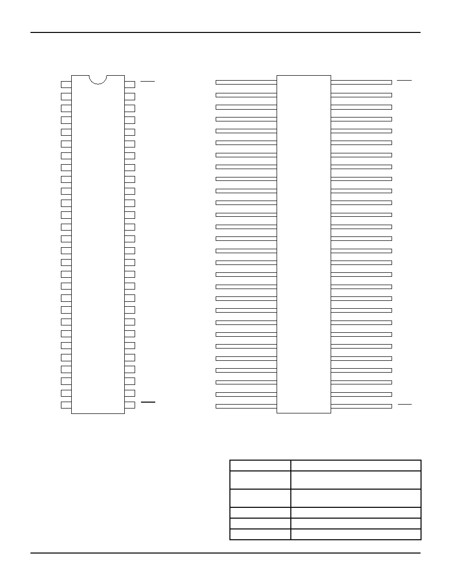
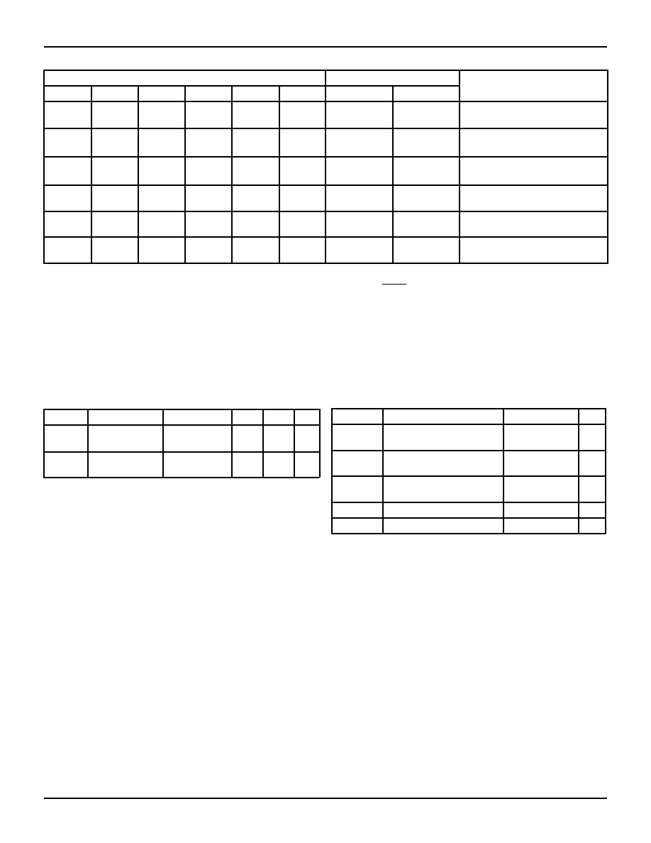
PIN CONFIGURATIONS
1
OEAB
1
CLKAB
1
SAB
GND
1
A
1
1
A
2
V
CC
1
A
3
1
A
4
GND
1
A
5
1
A
6
1
A
7
1
A
8
GND
2
A
1
2
A
2
V
CC
2
A
3
2
SAB
2
A
5
2
A
4
2
A
7
GND
2
A
8
2
CLKAB
2OEAB
2
A
6
1
B
1
1
B
2
GND
1
B
3
1
B
4
V
CC
1
B
5
1
B
6
1
OEBA
1
SBA
1
B
7
1
B
8
2
B
1
2
B
2
GND
2
B
3
2
B
4
V
CC
2
B
5
GND
1
CLKBA
2
B
7
2
B
6
2
B
8
GND
2
SBA
2
CLKBA
2
OEBA
47
37
38
39
40
41
42
43
44
45
46
33
34
35
36
56
55
49
50
51
52
53
54
48
1
2
3
4
5
6
7
8
9
10
12
13
14
15
16
17
18
19
20
11
21
22
23
24
29
30
31
32
25
26
27
28
3084 drw 04
CERPACK
TOP VIEW
E56-1
PIN DESCRIPTION
3084 tbl 01
Pin Names
Description
xAx
Data Register A Inputs
Data Register B Outputs
xBx
Data Register B Inputs
Data Register A Outputs
xCLKAB, xCLKBA Clock Pulse Inputs
xSAB, xSBA
Output Data Source Select Inputs
xOEAB, x
OEBA
Output Enable Inputs
1
B
1
1
B
2
GND
1
B
3
1
B
4
V
CC
1
B
5
1
B
6
1
OEBA
1
SBA
1
B
7
1
B
8
2
B
1
2
B
2
GND
2
B
3
2
B
4
V
CC
2
B
5
GND
1
CLKBA
2
B
7
2
B
6
2
B
8
GND
2
SBA
2
CLKBA
2
OEBA
1
OEAB
1
CLKAB
1
SAB
GND
1
A
1
1
A
2
V
CC
1
A
3
1
A
4
GND
1
A
5
1
A
6
1
A
7
1
A
8
GND
2
A
1
2
A
2
V
CC
2
A
3
2
SAB
2
A
5
2
A
4
2
A
7
GND
2
A
8
2
CLKAB
2OEAB
2
A
6
3084 drw 03
47
37
38
39
40
41
42
43
44
45
46
33
34
35
36
56
55
49
50
51
52
53
54
48
1
2
3
4
5
6
7
8
9
10
12
13
14
15
16
17
18
19
20
11
21
22
23
24
SSOP/
TSSOP/TVSOP
TOP VIEW
SO56-1
SO56-2
SO56-3
29
30
31
32
25
26
27
28
IDT54/74FCT163652/A/C
3.3V CMOS 16-BIT BUS TRANSCEIVER/REGISTER
MILITARY AND COMMERCIAL TEMPERATURE RANGES
8.7
3
FUNCTION TABLE
(2)
NOTES:
3084 tbl 03
1. The data output functions may be enabled or disabled by various signals at the xOEAB or xOEBA inputs.
Data input functions are always enabled, i.e. data at the bus pins will be stored on every LOW-to-HIGH
transition on the clock inputs.
2. Select control = L: clocks can occur simultaneously.
Select control = H: clocks must be staggered to load both registers.
3. H = HIGH Voltage Level
L = LOW Voltage Level
X = Don't Care
= LOW-to-HIGH Transition
CAPACITANCE
(T
A
= +25
∞
C, f = 1.0MHz)
ABSOLUTE MAXIMUM RATINGS
(1)
Inputs
Data I/O
(1)
Operation or Function
xOEAB
x
OEBA
OEBA
xCLKAB
xCLKBA
xSAB
xSBA
xAx
xBx
L
L
H
H
H or L
H or L
X
X
X
X
Input
Input
Isolation
Store A and B Data
X
H
H
H
H or L
X
X
(2)
X
X
Input
Input
Unspecified
(1)
Output
Store A, Hold B
Store A in Both Registers
L
L
X
L
H or L
X
X
X
X
(2)
Unspecified
(1)
Output
Input
Input
Hold A, Store B
Store B in both Registers
L
L
L
L
X
X
X
H or L
X
X
L
H
Output
Input
Real Time B Data to A Bus
Stored B Data to A Bus
H
H
H
H
X
H or L
X
X
L
H
X
X
Input
Output
Real Time A Data to B Bus
Stored A Data to B Bus
H
L
H or L
H or L
H
H
Output
Output
Stored A Data to B Bus and
Stored B Data to A Bus
Symbol
Parameter
(1)
Conditions
Typ.
Max.
Unit
C
IN
Input
Capacitance
V
IN
= 0V
3.5
6.0
pF
C
I/O
I/O
Capacitance
V
OUT
= 0V
3.5
8.0
pF
NOTE:
1. This parameter is measured at characterization but not tested.
3084 lnk 02
Symbol
Description
Max.
Unit
V
TERM(2)
Terminal Voltage with
Respect to GND
≠0.5 to +4.6
V
V
TERM(3)
Terminal Voltage with
Respect to GND
≠0.5 to +7.0
V
V
TERM(4)
Terminal Voltage with
Respect to GND
≠0.5 to
V
CC
+ 0.5
V
T
STG
Storage Temperature
≠65 to +150
∞
C
I
OUT
DC Output Current
≠60 to +60
mA
NOTES:
1. Stresses greater than those listed under ABSOLUTE MAXIMUM RAT-
INGS may cause permanent damage to the device. This is a stress rating
only and functional operation of the device at these or any other conditions
above those indicated in the operational sections of this specification is not
implied. Exposure to absolute maximum rating conditions for extended
periods may affect reliability.
2. Vcc terminals.
3. Input terminals.
4. Output and I/O terminals.
3084 lnk 04
8.7
4
IDT54/74FCT163652/A/C
3.3V CMOS 16-BIT BUS TRANSCEIVER/REGISTER
MILITARY AND COMMERCIAL TEMPERATURE RANGES
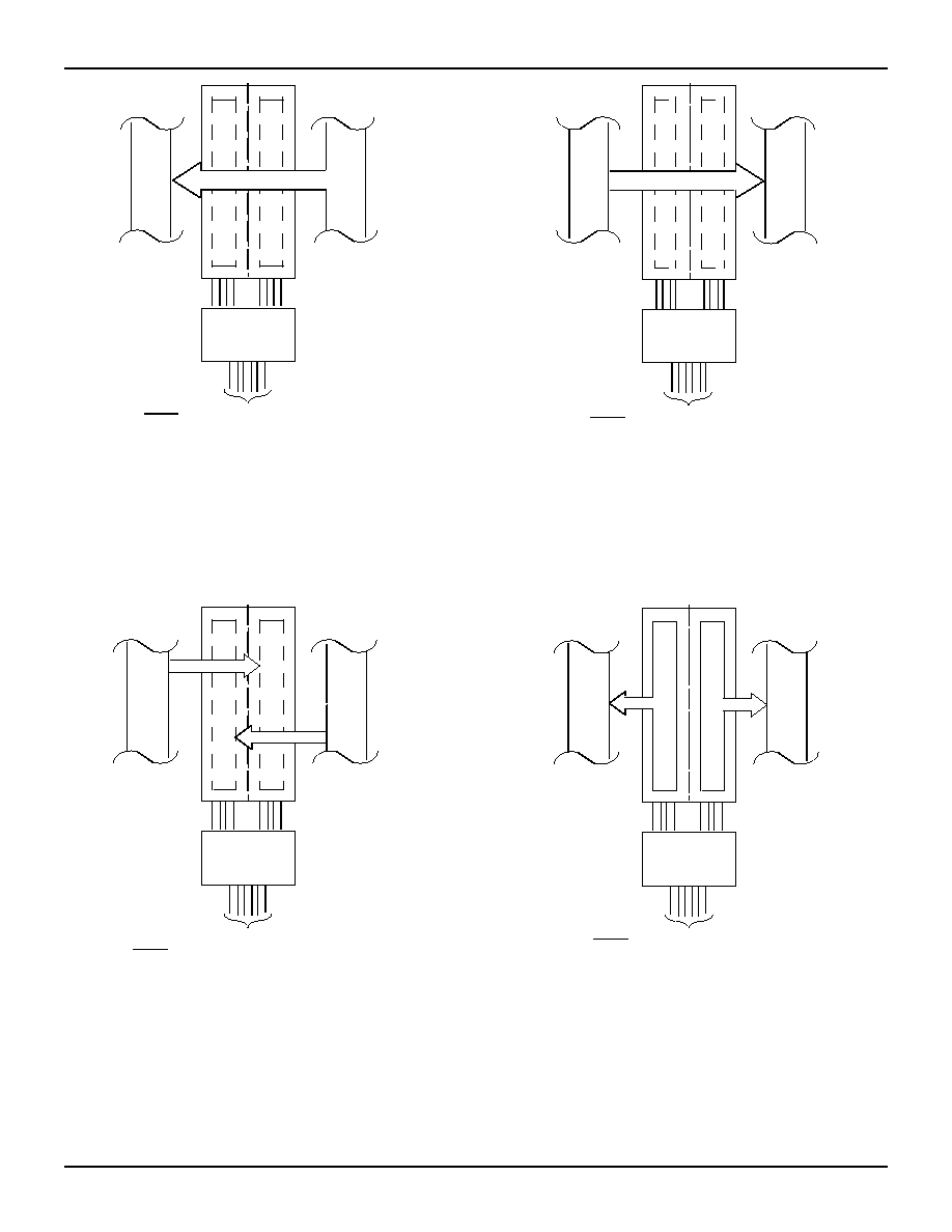
REAL-TIME TRANSFER
BUS B TO A
REAL-TIME TRANSFER
BUS A TO B
BUS
A
BUS
B
x
OEAB
x
OEBA
x
CLKAB
x
CLKBA
x
SAB
x
SBA
L
L
X
X
X
L
3084 drw 05
BUS
A
BUS
B
x
OEAB
x
OEBA
x
CLKAB
x
CLKBA
x
SAB
x
SBA
H
H
X
X
L
X
3084 drw 06
BUS
A
BUS
B
x
OEAB
x
OEBA
x
CLKAB
x
CLKBA
x
SAB
x
SBA
L
X
X
X
L
H
X
X
X
X
X
H
X
X
X
3084 drw 07
TRANSFER STORED
DATA TO A AND/OR B
STORAGE FROM
A AND/OR B
BUS
A
BUS
B
x
OEAB
x
OEBA
x
CLKAB
x
CLKBA
x
SAB
x
SBA
H
L
H or L
H
H or L
H
3084 drw 08
IDT54/74FCT163652/A/C
3.3V CMOS 16-BIT BUS TRANSCEIVER/REGISTER
MILITARY AND COMMERCIAL TEMPERATURE RANGES
8.7
5
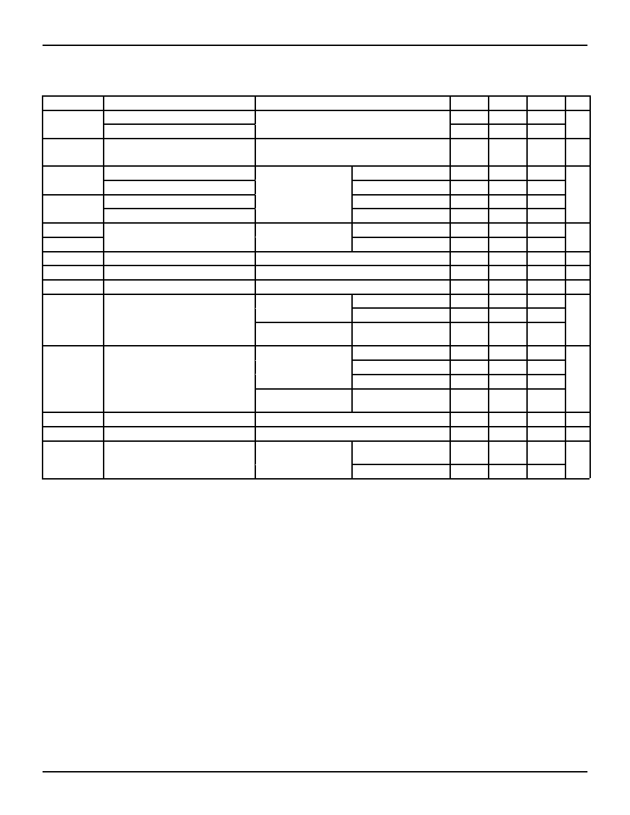
DC ELECTRICAL CHARACTERISTICS OVER OPERATING RANGE
Following Conditions Apply Unless Otherwise Specified:
Commercial: T
A
= ≠40
∞
C to +85
∞
C, V
CC
= 2.7V to 3.6V; Military: T
A
= ≠55
∞
C to +125
∞
C, V
CC
= 2.7V to 3.6V
3084 lnk 05
NOTES:
1. For conditions shown as Max. or Min., use appropriate value specified under Electrical Characteristics for the applicable device type.
2. Typical values are at Vcc = 3.3V, +25
∞
C ambient.
3. Not more than one output should be tested at one time. Duration of the test should not exceed one second.
4. This parameter is guaranteed but not tested.
5. V
OH
= V
CC
≠0.6V at rated current.
6. The test limit for this parameter is
±
5
µ
A at T
A
= ≠55
∞
C.
Symbol
Parameter
Test Conditions
(1)
Min.
Typ.
(2)
Max.
Unit
V
IH
Input HIGH Level (Input pins)
Guaranteed Logic HIGH Level
2.0
--
5.5
V
Input HIGH Level (I/O pins)
2.0
--
V
CC
+0.5
V
IL
Input LOW Level
Guaranteed Logic LOW Level
≠0.5
--
0.8
V
(Input and I/O pins)
I
I H
Input HIGH Current (Input pins)
(6)
V
CC
= Max.
V
I
= 5.5V
--
--
±
1
µ
A
Input HIGH Current (I/O pins)
(6)
V
I
= V
CC
--
--
±
1
I
I L
Input LOW Current (Input pins)
(6)
V
I
= GND
--
--
±
1
Input LOW Current (I/O pins)
(6)
V
I
= GND
--
--
±
1
I
OZH
High Impedance Output Current
V
CC
= Max.
V
O
= V
CC
--
--
±
1
µ
A
I
OZL
(3-State Output pins)
(6)
V
O
= GND
--
--
±
1
V
IK
Clamp Diode Voltage
V
CC
= Min., I
IN
= ≠18mA
--
≠
0.7
≠
1.2
V
I
ODH
Output HIGH Current
V
CC
= 3.3V, V
IN
= V
IH
or V
IL,
V
O
= 1.5V
(3)
≠36
≠60
≠110
mA
I
ODL
Output LOW Current
V
CC
= 3.3V, V
IN
= V
IH
or V
IL,
V
O
= 1.5V
(3)
50
90
200
mA
V
OH
Output HIGH Voltage
V
CC
= Min.
I
OH
= ≠0.1mA
V
CC
≠
0.2
--
--
V
V
IN
= V
IH
or V
IL
I
OH
= ≠3mA
2.4
3.0
--
V
CC
= 3.0V
V
IN
= V
IH
or V
IL
I
OH
= ≠6mA MIL.
I
OH
= ≠8mA COM'L.
2.4
(5)
3.0
--
V
OL
Output LOW Voltage
V
CC
= Min.
I
OL
= 0.1mA
--
--
0.2
V
V
IN
= V
IH
or V
IL
I
OL
= 16mA
--
0.2
0.4
I
OL
= 24mA
--
0.3
0.55
V
CC
= 3.0V
V
IN
= V
IH
or V
IL
I
OL
= 24mA
--
0.3
0.50
I
OS
Short Circuit Current
(4)
V
CC
= Max., V
O
= GND
(3)
≠60
≠
135
≠240
mA
V
H
Input Hysteresis
--
--
150
--
mV
I
CCL
I
CCH
Quiescent Power Supply Current
V
CC
= Max.,
V
IN
= GND or V
CC
COM'L.
--
0.1
10
µ
A
I
CCZ
MIL.
--
0.1
100