
1
IDT54/74FCT16373T/AT/CT/ET
FAST CMOS 16-BIT TRANSPARENT LATCH
MILITARY AND COMMERCIAL TEMPERATURE RANGES
AUGUST 1999
1999 Integrated Device Technology, Inc.
DSC-5454/-
c
IDT54/74FCT16373T/AT/CT/ET
MILITARY AND COMMERCIAL TEMPERATURE RANGES
FAST CMOS 16-BIT
TRANSPARENT
LATCH
DESCRIPTION:
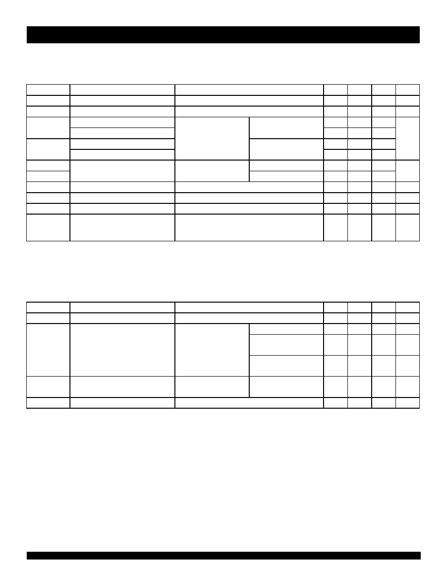
The FCT16373T/AT/CT/ET 16-bit transparent D-type latches are built
using advanced dual metal CMOS technology. These high-speed, low-
power latches are ideal for temporary storage of data. They can be used
for implementing memory address latches, I/O ports, and bus drivers. The
Output Enable and Latch Enable controls are organized to operate each
device as two 8-bit latches, or one 16-bit latch. Flow-through organization
of signal pins simplifies layout. All inputs are designed with hysteresis for
improved noise margin.
The FCT16373T/AT/CT/ET is ideally suited for driving high-capaci-
tance loads and low-impedance backplanes. The output buffers are
designed with power off disable capability to allow "live insertion" of boards
when used as backplane drivers.
FUNCTIONAL BLOCK DIAGRAM
2
O
1
2
OE
2
LE
2
D
1
TO SEVEN OTHER CHANN ELS
C
D
1
OE
1
LE
1
O
1
1
D
1
TO SEVEN OTHER CHANN ELS
C
D
FEATURES:
-
0.5 MICRON CMOS Technology
-
High-speed, low-power CMOS replacement for ABT functions
-
Typical t
SK
(o) (Output Skew) < 250ps
-
Low input and output leakage
1� A (max.)
-
ESD > 2000V per MIL-STD-883, Method 3015; > 200V using
machine model (C = 200pF, R = 0)
-
25 mil pitch SSOP, 19.6 mil pitch TSSOP,15.7 mil pitch TVSOP and
25 mil pitch CERPACK packages
-
Extended commercial range of -40�C to +85�C
-
V
CC
= 5V �10%
-
High drive outputs (-32mA I
OH
, 64mA I
OL
)
-
Power off disable outputs permit "live insertion"
-
Typical V
OLP
(Output Ground Bounce) < 1.0V at V
CC
= 5V, T
A
=
25�C

2
MILITARY AND COMMERCIAL TEMPERATURE RANGES
IDT54/74FCT16373T/AT/CT/ET
FAST CMOS 16-BIT TRANSPARENT LATCH
SSOP/ TSSOP/ TVSOP/ CERPACK
TOP VIEW
PIN CONFIGURATION
1
O
1
GND
1
O
3
V
CC
1
OE
GND
2
O
2
GND
V
CC
GND
1
O
2
1
O
4
1
O
5
1
O
6
1
O
7
1
O
8
2
O
1
2
O
3
2
O
4
2
O
5
2
O
7
2
O
8
2
O
6
2
OE
1
LE
1
D
1
1
D
2
GND
1
D
3
1
D
4
V
CC
1
D
5
1
D
6
1
D
7
1
D
8
2
D
1
2
D
2
2
D
3
2
D
4
V
CC
2
D
5
2
D
7
2
D
8
2
D
6
2
LE
GND
GND
GND
39
29
30
31
32
33
34
35
36
37
38
25
26
27
28
48
47
41
42
43
44
45
46
40
1
2
3
4
5
6
7
8
9
10
12
13
14
15
16
17
18
19
20
11
21
22
23
24
SO48-1
SO48-2
SO48-3
E48-1
ABSOLUTE MAXIMUM RATINGS
(1)
Symbol
Description
Max
Unit
V
TERM(2)
Terminal Voltage with Respect to GND
�0.5 to +7
V
V
TERM(3)
Terminal Voltage with Respect to GND
�0.5 to V
CC
+0.5
V
T
STG
Storage Temperature
�65 to +150
�C
I
OUT
DC Output Current
�60 to +120
mA
5v16-link
NOTES:
1. Stresses greater than those listed under ABSOLUTE MAXIMUM
RATINGS may cause permanent damage to the device. This is a
stress rating only and functional operation of the device at these or
any other conditions above those indicated in the operational sections
of this specification is not implied. Exposure to absolute maximum
rating conditions for extended periods may affect reliability.
2. All device
terminals except FCT162XXXT Output and I/O terminals.
3. Output and I/O terminals for FCT162XXXT.
CAPACITANCE (T
A
= +25
O
C, f = 1.0MHz)
Symbol
Parameter
(1)
Conditions
Typ.
Max.
Unit
C
IN
Input Capacitance
V
IN
= 0V
3.5
6
pF
C
OUT
Output Capacitance
V
OUT
= 0V
3.5
8
pF
5v16-link
NOTE:
1. This parameter is measured at characterization but not tested.
NOTE:
1. H = HIGH voltage level
L = LOW voltage level
X = Don't care
Z = High-impedance
PIN DESCRIPTION
Pin Names
Description
xDx
Data Inputs
xLE
Latch Enable Input (Active HIGH)
x
OE
Output Enable Input (Active LOW)
xOx
3-State Outputs
FUNCTION TABLE
(1)
Inputs
Outputs
xDx
xLE
xOE
xOx
H
H
L
H
L
H
L
L
X
X
H
Z
3
IDT54/74FCT16373T/AT/CT/ET
FAST CMOS 16-BIT TRANSPARENT LATCH
MILITARY AND COMMERCIAL TEMPERATURE RANGES
DC ELECTRICAL CHARACTERISTICS OVER OPERATING RANGE
Following Conditions Apply Unless Otherwise Specified:
Commercial: T
A
= -40�C to +85�C, V
CC
= 5.0V �10%; Military: T
A
= -55�C to +125�C, V
CC
= 5.0V �10%
Symbol
Parameter
Test Conditions
(1)
Min.
Typ.
(2)
Max.
Unit
V
IH
Input HIGH Level
Guaranteed Logic HIGH Level
2
--
--
V
V
IL
Input LOW Level
Guaranteed Logic LOW Level
--
--
0.8
V
I
IH
Input HIGH Current (Input pins)
(5)
V
CC
= Max.
V
I
= V
CC
--
--
�
1
� A
Input HIGH Current (I/O pins)
(5)
--
--
�
1
I
IL
Input LOW Current (Input pins)
(5)
V
I
= GND
--
--
�
1
Input LOW Current (I/O pins)
(5)
--
--
�
1
I
OZH
High Impedance Output Current
V
CC
= Max.
V
O
= 2.7V
--
--
�
1
� A
I
OZL
(3-State Output pins)
(5)
V
O
= 0.5V
--
--
�
1
V
IK
Clamp Diode Voltage
V
CC
= Min., I
IN
= �18mA
--
�0.7
�1.2
V
I
OS
Short Circuit Current
V
CC
= Max., V
O
= GND
(3)
�80
�140
�250
mA
V
H
Input Hysteresis
--
--
100
--
mV
I
CCL
I
CCH
I
CCZ
Quiescent Power Supply Current
V
CC
= Max.
V
IN
= GND or V
CC
--
5
500
� A
5v16-link
OUTPUT DRIVE CHARACTERISTICS
Symbol
Parameter
Test Conditions
(1)
Min.
Typ.
(2)
Max.
Unit
I
O
Output Drive Current
V
CC
= Max., V
O
= 2.5V
(3)
�50
--
�180
mA
V
OH
Output HIGH Voltage
V
CC
= Min.
I
OH
= �3mA
2.5
3.5
--
V
V
IN
= V
IH
or V
IL
I
OH
= �12mA MIL
2.4
3.5
--
V
I
OH
= �15mA COM'L
I
OH
= �24mA MIL.
2
3
--
V
I
OH
= �32mA COM'L
(4)
V
OL
Output LOW Voltage
V
CC
= Min.
I
OL
= 48mA MIL
--
0.2
0.55
V
V
IN
= V
IH
or V
IL
I
OL
= 64mA COM'L
I
OFF
Input/Output Power Off Leakage
(5)
V
CC
= 0V, V
IN
or V
O
4.5V
--
--
�1
� A
NOTES:
1. For conditions shown as Max. or Min., use appropriate value specified under Electrical Characteristics for the applicable device type.
2. Typical values are at V
CC
= 5.0V, +25�C ambient.
3. Not more than one output should be shorted at one time. Duration of the test should not exceed one second.
4. Duration of the condition can not exceed one second.
5. The test limit for this parameter is �5�A at T
A
= -55�C.
4
MILITARY AND COMMERCIAL TEMPERATURE RANGES
IDT54/74FCT16373T/AT/CT/ET
FAST CMOS 16-BIT TRANSPARENT LATCH
NOTES:
1. For conditions shown as Max. or Min., use appropriate value specified under Electrical Characteristics for the applicable device type.
2. Typical values are at V
CC
= 5.0V, +25�C ambient.
3. Per TTL driven input (V
IN
= 3.4V). All other inputs at V
CC
or GND.
4. This parameter is not directly testable, but is derived for use in Total Power Supply Calculations.
5. Values for these conditions are examples of the I
CC
formula. These limits are guaranteed but not tested.
6. I
C
= I
QUIESCENT
+ I
INPUTS
+ I
DYNAMIC
I
C
= I
CC
+
I
CC
D
H
N
T
+ I
CCD
(f
CP
N
CP
/2 + f
i
N
i
)
I
CC
= Quiescent Current (I
CCL
,
I
CCH
and I
CCZ
)
I
CC
= Power Supply Current for a TTL High Input (V
IN
= 3.4V)
D
H
= Duty Cycle for TTL Inputs High
N
T
= Number of TTL Inputs at D
H
I
CCD
= Dynamic Current Caused by an Input Transition Pair (HLH or LHL)
f
CP
= Clock Frequency for Register Devices (Zero for Non-Register Devices)
N
CP
= Number of Clock Inputs at f
CP
f
i
= Input Frequency
N
i
= Number of Inputs at f
i
POWER SUPPLY CHARACTERISTICS
Symbol
Parameter
Test Conditions
(1)
Min.
Typ.
(2)
Max.
Unit
I
CC
Quiescent Power Supply Current
TTL Inputs HIGH
V
CC
= Max.
V
IN
= 3.4V
(3)
--
0.5
1.5
mA
I
CCD
Dynamic Power Supply Current
(4)
V
CC
= Max.
Outputs Open
x
OE = GND
One Input Toggling
50% Duty Cycle
V
IN
= V
CC
V
IN
= GND
--
60
100
� A/
MHz
I
C
Total Power Supply Current
(6)
V
CC
= Max.
Outputs Open
fi =10MHz
V
IN
= V
CC
V
IN
= GND
--
0.6
1.5
mA
50% Duty Cycle
x
OE = GND
xLE
=
V
CC
One Bit Toggling
V
IN
= 3.4V
V
IN
= GND
--
0.9
2.3
V
CC
= Max.
Outputs Open
fi = 2.5MHz
V
IN
= V
CC
V
IN
= GND
--
2.4
4.5
(5)
50% Duty Cycle
x
OE = GND
xLE = V
CC
Sixteen Bits Toggling
V
IN
= 3.4V
V
IN
= GND
--
6.4
16.5
(5)
5
IDT54/74FCT16373T/AT/CT/ET
FAST CMOS 16-BIT TRANSPARENT LATCH
MILITARY AND COMMERCIAL TEMPERATURE RANGES
NOTES:
1. See test circuit and waveforms.
2. Minimum limits are guaranteed but not tested on Propagation Delays.
3. Skew between any two outputs of the same package switching in the same direction. This parameter is guaranteed by design.
4. This limit is guaranteed but not tested.
SWITCHING CHARACTERISTICS OVER OPERATING RANGE
FCT16373T
FCT16373AT
Com'l.
Mil.
Com'l.
Mil.
Symbol
Parameter
Condition
(1)
Min
.
(2)
Max
.
Min
.
(2)
Max
.
Min
.
(2)
Max
.
Min
.
(2)
Max
.
Unit
t
PLH
t
PHL
Propagation Delay
xDx to xOx
C
L
= 50pF
R
L
= 500
1.5
8
1.5
8.5
1.5
5.2
1.5
5.6
ns
t
PLH
t
PHL
Propagation Delay
xLE to xOx
2
13
2
15
2
8.5
2
9.8
ns
t
PZH
t
PZL
Output Enable Time
1.5
12
1.5
13.5
1.5
6.5
1.5
7.5
ns
t
PHZ
t
PLZ
Output Disable Time
1.5
7.5
1.5
10
1.5
5.5
1.5
6.5
ns
t
SU
Set-up Time HIGH or LOW, xDx to xLE
2
--
2
--
2
--
2
--
ns
t
H
Hold Time HIGH or LOW, xDx to xLE
1.5
--
1.5
--
1.5
--
1.5
--
ns
t
W
xLE Pulse Width HIGH
6
--
6
--
5
--
6
--
ns
t
SK
(o)
Output Skew
(3)
--
0.5
--
0.5
--
0.5
--
0.5
ns
FCT16373CT
FCT16373ET
Com'l.
Mil.
Com'l.
Mil.
Symbol
Parameter
Condition
(1)
Min
.
(2)
Max
.
Min
.
(2)
Max
.
Min
.
(2)
Max
.
Min
.
(2)
Max
.
Unit
t
PLH
t
PHL
Propagation Delay
xDx to xOx
C
L
= 50pF
R
L
= 500
1.5
4.2
1.5
5.1
1.5
3.4
--
--
ns
t
PLH
t
PHL
Propagation Delay
xLE to xOx
2
5.5
2
8
1.5
3.7
--
--
ns
t
PZH
t
PZL
Output Enable Time
1.5
5.5
1.5
6.3
1.5
4.4
--
--
ns
t
PHZ
t
PLZ
Output Disable Time
1.5
5
1.5
5.9
1.5
3.6
--
--
ns
t
SU
Set-up Time HIGH or LOW, xDx to xLE
2
--
2
--
1
--
--
--
ns
t
H
Hold Time HIGH or LOW, xDx to xLE
1.5
--
1.5
--
1
--
--
--
ns
t
W
xLE Pulse Width HIGH
5
--
6
--
3
(4)
--
--
--
ns
t
SK
(o)
Output Skew
(3)
--
0.5
--
0.5
--
0.5
--
--
ns