Integrated Device Technology, Inc.
MILITARY AND COMMERCIAL TEMPERATURE RANGES
OCTOBER 1994
©
1995 Integrated Device Technology, Inc.
6.7
DSC-4219/4
DESCRIPTION:
The IDT54/74FCT161T/163T, IDT54/74FCT161AT/ 163AT
and IDT54/74FCT161CT/163CT are high-speed synchro-
nous modulo-16 binary counters built using an advanced dual
metal CMOS technology. They are synchronously preset-
table for application in programmable dividers and have two
types of count enable inputs plus a terminal count output for
versatility in forming synchronous multi-stage counters. The
IDT54/74FCT161T/AT/CT have asynchronous Master Reset
inputs that override all other inputs and force the outputs LOW.
The IDT54/74FCT163T/AT/CT have Synchronous Reset in-
puts that override counting and parallel loading and allow the
outputs to be simultaneously reset on the rising edge of the
clock.
FAST CMOS
SYNCHRONOUS
PRESETTABLE
BINARY COUNTERS
IDT54/74FCT161T/AT/CT
IDT54/74FCT163T/AT/CT
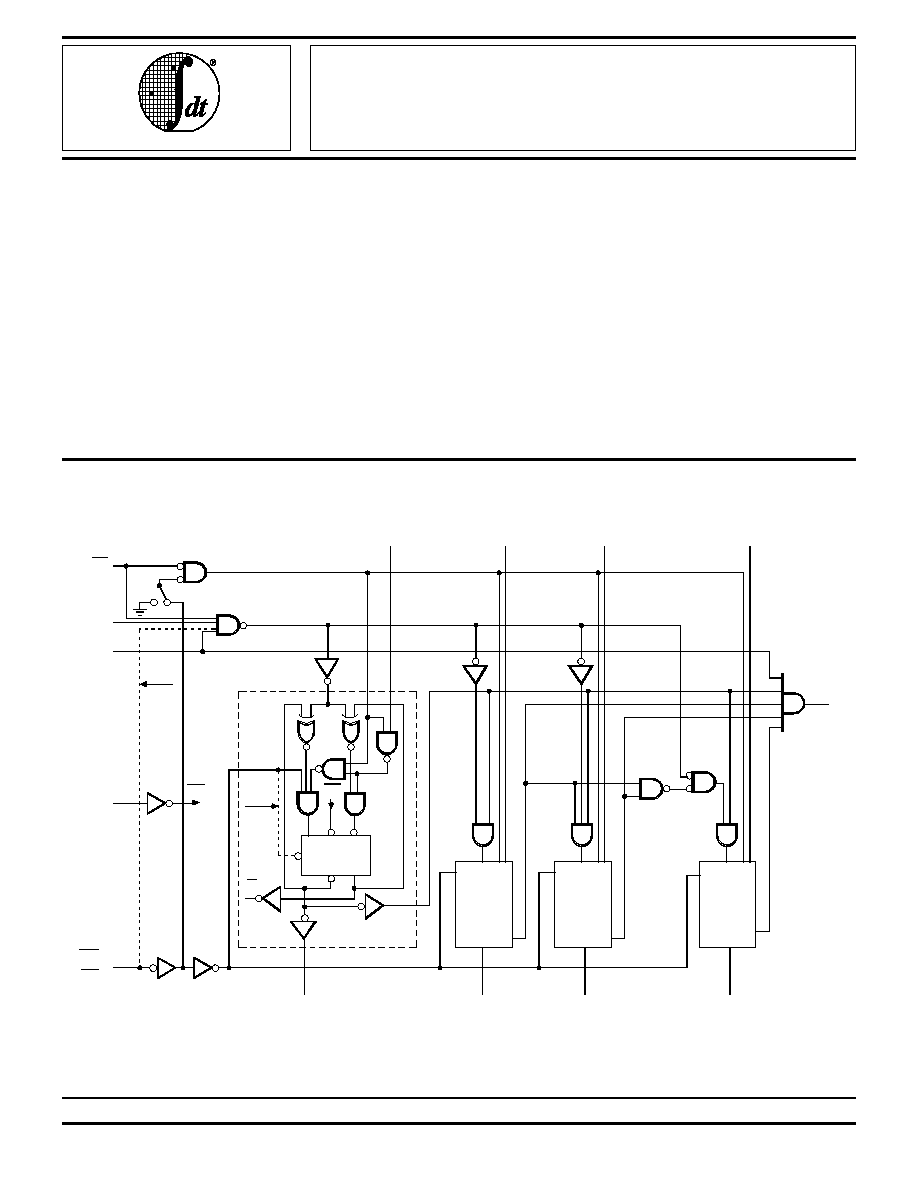
FUNCTIONAL BLOCK DIAGRAMS
2611 drw 01
Q
0
D CP D
Q
Q
C
D
CP
161
ONLY
DETAIL
A
DETAIL
A
DETAIL
A
'161
'163
PE
CEP
CET
CP
MR ('161)
SR ('163)
Q
0
Q
1
Q
2
Q
3
Q
0
DETAIL A
P
0
P
1
P
2
P
3
TC
163
ONLY
CP
1
FEATURES:
∑ Std., A and C speed grades
∑ Low input and output leakage
1
µ
A (max.)
∑ CMOS power levels
∑ True TTL input and output compatibility
≠ V
OH
= 3.3V (typ.)
≠ V
OL
= 0.3V (typ.)
∑ High drive outputs (-15mA I
OH
, 48mA I
OL
)
∑ Meets or exceeds JEDEC standard 18 specifications
∑ Product available in Radiation Tolerant and Radiation
Enhanced versions
∑ Military product compliant to MIL-STD-883, Class B
and DESC listed (dual marked)
∑ Available in DIP, SOIC, QSOP, CERPACK and LCC
packages
The IDT logo is a registered trademark of Integrated Device Technology, Inc.

IDT54/74FCT161T/AT/CT, IDT54/74FCT163T/AT/CT
FAST CMOS SYNCHRONOUS PRESETTABLE BINARY COUNTERS
MILITARY AND COMMERCIAL TEMPERATURE RANGES
6.7
2
PIN CONFIGURATIONS
IDT54/74FCT861 10-BIT TRANSCEIVERS
PIN DESCRIPTION
Pin Names
Description
CEP
Count Enable Parallel Input
CET
Count Enable Trickle Input
CP
Clock Pulse Input (Active Rising Edge)
MR
(`161)
Asynchronous Master Reset Input (Active LOW)
SR
(`163)
Synchronous Reset Input (Active LOW)
P
0-3
Parallel Data Inputs
PE
Parallel Enable Input (Active LOW)
Q
0-3
Flip-Flop Outputs
TC
Terminal Count Output
FUNCTION TABLE
(2)
Action on the Rising
SR
SR
(1)
PE
PE
CET
CEP
Clock Edge(s)
L
X
X
X
Reset (Clear)
H
L
X
X
Load (P
n
Q
n
)
H
H
H
H
Count (Increment)
H
H
L
X
No Change (Hold)
H
H
X
L
No Change (Hold)
2611 tbl 01
ABSOLUTE MAXIMUM RATINGS
(1)
Symbol
Rating
Commercial
Military
Unit
V
TERM(2)
Terminal Voltage
with Respect to
GND
≠0.5 to +7.0
≠0.5 to +7.0
V
V
TERM(3)
Terminal Voltage
with Respect to
GND
≠0.5 to
V
CC
+0.5
≠0.5 to
V
CC
+0.5
V
T
A
Operating
Temperature
0 to +70
≠55 to +125
∞
C
T
BIAS
Temperature
Under Bias
≠55 to +125
≠65 to +135
∞
C
T
STG
Storage
Temperature
≠55 to +125
≠65 to +150
∞
C
P
T
Power Dissipation
0.5
0.5
W
I
OUT
DC Output
Current
≠60 to +120 ≠60 to +120 mA
CAPACITANCE
(T
A
= +25
∞
C, f = 1.0MHz)
Symbol
Parameter
(1)
Conditions
Typ.
Max. Unit
C
IN
Input
Capacitance
V
IN
= 0V
6
10
pF
C
OUT
Output
Capacitance
V
OUT
= 0V
8
12
pF
NOTE:
1. This parameter is measured at characterization but not tested.
NOTES:
2611 tbl 02
1. 163 only.
2. H = HIGH Voltage Level, L = LOW Voltage Level, X = Don't Care.
2611 lnk 04
NOTES:
1. Stresses greater than those listed under ABSOLUTE MAXIMUM RAT-
INGS may cause permanent damage to the device. This is a stress rating
only and functional operation of the device at these or any other condi-
tions above those indicated in the operational sections of this specifica-
tion is not implied. Exposure to absolute maximum rating conditions for
extended periods may affect reliability. No terminal voltage may exceed
V
CC
by +0.5V unless otherwise noted.
2. Input and V
CC
terminals only.
3. Outputs and I/O terminals only.
2611 lnk 03
GND
CEP
5
6
7
8
1
2
3
4
16
15
14
13
12
11
10
9
Vcc
P16-1,
D16-1,
S016-1,
S016-7
&
E16-1
P
0
*R
P
1
P
2
P
3
CP
TC
Q
0
Q
1
Q
2
Q
3
CET
PE
2611 drw 02
2611 drw 03
4
5
6
7
8
L20-2
18
17
16
15
14
INDEX
GND
NC
NC
NC
NC
*R
CP
Vcc
TC
CEP
CET
PE
P
0
P
1
P
2
P
3
Q
0
Q
1
Q
2
Q
3
9 10 11 12 13
3
2
1
20 19
LCC
TOP VIEW
DIP/SOIC/QSOP/CERPACK
TOP VIEW
*
MR
for '161
*
SR
for `163

IDT54/74FCT161T/AT/CT, IDT54/74FCT163T/AT/CT
FAST CMOS SYNCHRONOUS PRESETTABLE BINARY COUNTERS
MILITARY AND COMMERCIAL TEMPERATURE RANGES
6.7
3
DC ELECTRICAL CHARACTERISTICS OVER OPERATING RANGE
Following Conditions Apply Unless Otherwise Specified:
Commercial: T
A
= 0
∞
C to +70
∞
C, V
CC
= 5.0V
±
5%; Military: T
A
= ≠55
∞
C to +125
∞
C, V
CC
= 5.0V
±
10%
Symbol
Parameter
Test Conditions
(1)
Min.
Typ.
(2)
Max.
Unit
V
IH
Input HIGH Level
Guaranteed Logic HIGH Level
COM'L
(5)
2.0V
--
--
V
MIL
2.7V
--
--
V
V
IL
Input LOW Level
Guaranteed Logic LOW Level
--
--
0.8
V
I
IH
Input HIGH Current
(4)
V
CC
= Max.
V
I
= 2.7V
--
--
±
1
µ
A
I
IL
Input LOW Current
(4)
V
CC
= Max.
V
I
= 0.5V
--
--
±
1
µ
A
I
I
Input HIGH Current
(4)
V
CC
= Max., V
I
= V
CC
(Max.)
--
--
±
1
µ
A
V
IK
Clamp Diode Voltage
V
CC
= Min., I
N
= ≠18mA
--
≠0.7
≠1.2
V
I
OS
Short Circuit Current
V
CC
= Max.
(3)
, V
O
= GND
≠60
≠120
≠225
mA
V
OH
Output HIGH Voltage
V
CC
= Min.
I
OH
= ≠6mA MIL.
2.4
3.3
--
V
V
IN
= V
IH
or V
IL
I
OH
= ≠8mA COM'L.
I
OH
= ≠12mA MIL.
2.0
3.0
--
V
I
OH
= ≠15mA COM'L.
V
OL
Output LOW Voltage
V
CC
= Min.
I
OL
= 32mA MIL.
--
0.3
0.5
V
V
IN
= V
IH
or V
IL
I
OL
= 48mA COM'L.
V
H
Input Hysteresis
--
--
200
--
mV
I
CC
Quiescent Power
V
CC
= Max.
--
0.01
1
mA
Supply Current
V
IN
= GND or V
CC
NOTES:
2611 tbl 05
1. For conditions shown as Max. or Min., use appropriate value specified under Electrical Characteristics for the applicable device type.
2. Typical values are at V
CC
= 5.0V, +25
∞
C ambient.
3. Not more than one output should be shorted at one time. Duration of the short circuit test should not exceed one second.
4. The test limit for this parameter is
±
5
µ
A at T
A
= -55
∞
C.
5. Clock pin requires a minimum V
IH
of 2.5V.
IDT54/74FCT161T/AT/CT, IDT54/74FCT163T/AT/CT
FAST CMOS SYNCHRONOUS PRESETTABLE BINARY COUNTERS
MILITARY AND COMMERCIAL TEMPERATURE RANGES
6.7
4
POWER SUPPLY CHARACTERISTICS
Symbol
Parameter
Test Conditions
(1)
Min.
Typ.
(2)
Max.
Unit
I
CC
Quiescent Power Supply Current
V
CC
= Max.
--
0.5
2.0
mA
TTL Inputs HIGH
V
IN
= 3.4V
(3)
I
CCD
Dynamic Power Supply Current
(4)
V
CC
= Max., Outputs Open
V
IN
= V
CC
--
0.15
0.25
mA/
Load Mode
V
IN
= GND
MHz
CEP = CET =
PE
= GND
MR
or
SR
= V
CC
One Input Toggling
50% Duty Cycle
I
C
Total Power Supply Current
(6)
V
CC
= Max., Outputs Open
V
IN
= V
CC
--
1.5
3.5
mA
Load Mode
V
IN
= GND
f
CP
= 10MHz
50% Duty Cycle
CEP = CET =
PE
= GND
V
IN
= 3.4V
--
2.0
5.5
MR
or
SR
= V
CC
V
IN
= GND
One Bit Toggling
at f
i
= 5MHz
50% Duty Cycle
V
CC
= Max., Outputs Open
V
IN
= V
CC
--
3.8
7.3
(5)
Load Mode
V
IN
= GND
f
CP
= 10MHz
50% Duty Cycle
CEP = CET =
PE
= GND
V
IN
= 3.4V
--
5.0
12.3
(5)
MR
or
SR
= V
CC
V
IN
= GND
Four Bits Toggling
at f
i
= 5MHz
50% Duty Cycle
2611 tbl 06
NOTES:
1. For conditions shown as Max. or Min., use appropriate value specified under Electrical Characteristics for the applicable device type.
2. Typical values are at V
CC
= 5.0V, +25
∞
C ambient.
3. Per TTL driven input (V
IN
= 3.4V). All other inputs at V
CC
or GND.
4. This parameter is not directly testable, but is derived for use in Total Power Supply Calculations.
5. Values for these conditions are examples of the I
CC
formula. These limits are guaranteed but not tested.
6. I
C
= I
QUIESCENT
+ I
INPUTS
+ I
DYNAMIC
I
C
= I
CC
+
I
CC
D
H
N
T
+ I
CCD
(f
CP/
2 + f
i
N
i
)
I
CC
= Quiescent Current
I
CC
= Power Supply Current for a TTL High Input (V
IN
= 3.4V)
D
H
= Duty Cycle for TTL Inputs High
N
T
= Number of TTL Inputs at D
H
I
CCD
= Dynamic Current Caused by an Input Transition Pair (HLH or LHL)
f
CP
= Clock Frequency for Register Devices (Zero for Non-Register Devices)
f
i
= Input Frequency
N
i
= Number of Inputs at f
i
All currents are in milliamps and all frequencies are in megahertz.

IDT54/74FCT161T/AT/CT, IDT54/74FCT163T/AT/CT
FAST CMOS SYNCHRONOUS PRESETTABLE BINARY COUNTERS
MILITARY AND COMMERCIAL TEMPERATURE RANGES
6.7
5
SWITCHING CHARACTERISTICS OVER OPERATING RANGE
IDT54/74FCT161T
IDT54/74FCT161AT
IDT54/74FCT161CT
IDT54/74FCT163T
IDT54/74FCT163AT
IDT54/74FCT163CT
Com'l.
Mil.
Com'l.
Mil.
Com'l
Mil.
Symbol
Parameter
Condition
(1)
Min.
(2)
Max. Min.
(2)
Max. Min.
(2)
Max. Min.
(2)
Max. Min.
(2)
Max. Min.
(2)
Max.
Unit
t
PLH
Propagation Delay
C
L
= 50pF
2.0
11.0
2.0
11.5
2.0
7.2
2.0
7.5
2.0
5.8
2.0
6.3
ns
t
PHL
CP to Q
n
R
L
= 500
(
PE
Input HIGH)
t
PLH
Propagation Delay
2.0
9.5
2.0
10.0
2.0
6.2
2.0
6.5
2.0
5.8
2.0
6.3
ns
t
PHL
CP to Q
n
(
PE
Input LOW)
t
PLH
Propagation Delay
2.0
15.0
2.0
16.5
2.0
9.8
2.0
10.8
2.0
7.4
2.0
8.3
ns
t
PHL
CP to TC
t
PLH
Propagation Delay
1.5
8.5
1.5
9.0
1.5
5.5
1.5
5.9
1.5
5.2
1.5
5.6
ns
t
PHL
CET to TC
t
PHL
Propagation Delay
2.0
13.0
2.0
14.0
2.0
8.5
2.0
9.1
2.0
6.0
2.0
6.6
ns
MR
to Q
n
('161)
t
PHL
Propagation Delay
2.0
11.5
2.0
12.5
2.0
7.5
2.0
8.2
2.0
7.0
2.0
7.7
ns
MR
to TC ('161)
t
SU
Set-up Time,
5.0
--
5.5
--
4.0
--
4.5
--
4.0
--
4.5
--
ns
HIGH or LOW
P
n
to CP
t
H
Hold Time,
1.5
--
2.0
--
1.5
--
2.0
--
1.5
--
2.0
--
ns
HIGH or LOW
P
n
to CP
t
SU
Set-up Time,
11.5
--
13.5
--
9.5
--
11.5
--
9.5
--
11.5
--
ns
HIGH or LOW
PE
or
SR
to CP
t
H
Hold Time,
1.5
--
1.5
--
1.5
--
1.5
--
1.5
--
1.5
--
ns
HIGH or LOW
PE
or
SR
to CP
t
SU
Set-up Time,
11.5
--
13.0
--
9.5
--
11.0
--
9.5
--
11.0
--
ns
HIGH or LOW
CEP or CET to CP
t
H
Hold Time,
0
--
0
--
0
--
0
--
0
--
0
--
ns
HIGH or LOW
CEP or CET to CP
t
W
Clock Pulse
5.0
--
5.0
--
4.0
(3)
--
4.0
(3)
--
4.0
(3)
--
4.0
(3)
--
ns
Width (Load)
HIGH or LOW
t
W
Clock Pulse
7.0
--
8.0
--
6.0
--
7.0
--
6.0
--
7.0
--
ns
Width (Count)
HIGH or LOW
t
W
MR
Pulse Width,
5.0
--
5.0
--
4.0
(3)
--
4.0
(3)
--
4.0
(3)
--
4.0
(3)
--
ns
LOW ('161)
t
REM
Recovery Time
6.0
--
6.0
--
5.0
--
5.0
--
5.0
--
5.0
--
ns
MR
to CP ('161)
NOTES:
2611 tbl 07
1. See test circuits and waveforms.
2. Minimum limits are guaranteed but not tested on Propagation Delays.
3. This limit is guaranteed but not tested.
IDT54/74FCT161T/AT/CT, IDT54/74FCT163T/AT/CT
FAST CMOS SYNCHRONOUS PRESETTABLE BINARY COUNTERS
MILITARY AND COMMERCIAL TEMPERATURE RANGES
6.7
6
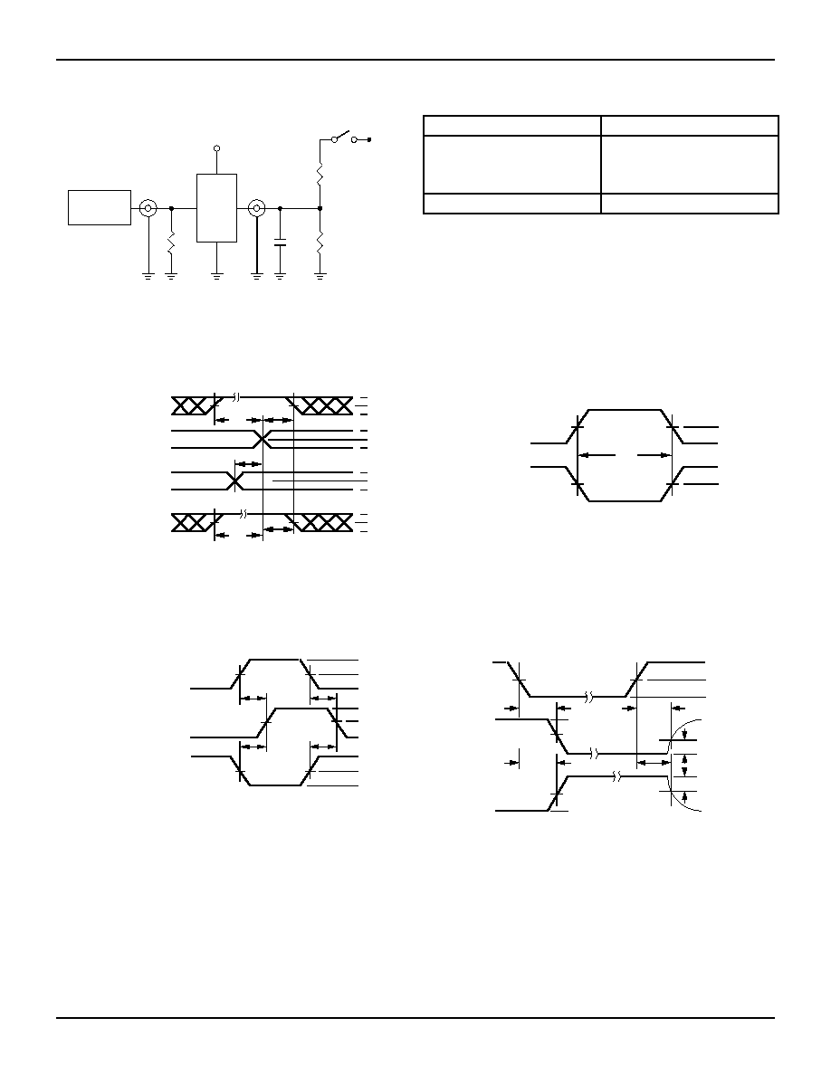
TEST CIRCUITS AND WAVEFORMS
TEST CIRCUITS FOR ALL OUTPUTS
ENABLE AND DISABLE TIMES
PROPAGATION DELAY
SET-UP, HOLD AND RELEASE TIMES
PULSE WIDTH
SWITCH POSITION
Pulse
Generator
R
T
D.U.T.
V
CC
V
IN
C
L
V
OUT
50pF
500
500
7.0V
3V
1.5V
0V
3V
1.5V
0V
3V
1.5V
0V
3V
1.5V
0V
DATA
INPUT
TIMING
INPUT
ASYNCHRONOUS CONTROL
PRESET
CLEAR
ETC.
SYNCHRONOUS CONTROL
t
SU
t
H
t
REM
t
SU
t
H
HIGH-LOW-HIGH
PULSE
LOW-HIGH-LOW
PULSE
t
W
1.5V
1.5V
SAME PHASE
INPUT TRANSITION
3V
1.5V
0V
1.5V
V
OH
t
PLH
OUTPUT
OPPOSITE PHASE
INPUT TRANSITION
3V
1.5V
0V
t
PLH
t
PHL
t
PHL
V
OL
CONTROL
INPUT
3V
1.5V
0V
3.5V
0V
OUTPUT
NORMALLY
LOW
OUTPUT
NORMALLY
HIGH
SWITCH
CLOSED
SWITCH
OPEN
V
OL
0.3V
0.3V
t
PLZ
t
PZL
t
PZH
t
PHZ
3.5V
0V
1.5V
1.5V
ENABLE
DISABLE
V
OH
PRESET
CLEAR
CLOCK ENABLE
ETC.
Test
Switch
Disable Low
Enable Low
Closed
All Other Tests
Open
Open Drain
DEFINITIONS:
C
L
=
Load capacitance: includes jig and probe capacitance.
R
T
=
Termination resistance: should be equal to Z
OUT
of the Pulse
Generator.
2611 lnk 08
2611 drw 04
2611 drw 05
2611 drw 06
2611 drw 07
2611 drw 08
NOTES:
1. Diagram shown for input Control Enable-LOW and input Control Disable-
HIGH
2. Pulse Generator for All Pulses: Rate
1.0MHz; t
F
2.5ns; t
R
2.5ns

IDT54/74FCT161T/AT/CT, IDT54/74FCT163T/AT/CT
FAST CMOS SYNCHRONOUS PRESETTABLE BINARY COUNTERS
MILITARY AND COMMERCIAL TEMPERATURE RANGES
6.7
7
ORDERING INFORMATION
2611 drw 09
Synchronous Binary Counter
with Asynchronous Master Reset
X
Temperature
Range
XXXX
Device
Type
X
Package
X
Process
Blank
Commercial
B
MIL-STD-883, Class B
P
D
L
SO
E
Q
Plastic DIP
CERDIP
Leadless Chip Carrier
Small Outline IC
CERPACK
Quarter-size Small Outline Package
-55
∞
C to +125
∞
C
0
∞
to +70
∞
C
54
74
FCT
IDT
161T
163T
161AT
163AT
X
Family
High Drive
Blank