Integrated Device Technology, Inc.
MILITARY AND COMMERCIAL TEMPERATURE RANGES
SEPTEMBER 1996
©
1996 Integrated Device Technology, Inc.
5.12
DSC-2618/7
1
The IDT logo is a registered trademark of Integrated Device Technology, Inc.
FAST CMOS
16-BIT LATCHED
TRANSCEIVER
FEATURES:
∑ Common features:
≠
0.5 MICRON CMOS Technology
≠
High-speed, low-power CMOS replacement for
ABT functions
≠
Typical t
SK
(o) (Output Skew) < 250ps
≠
Low input and output leakage
1
µ
A (max.)
≠
ESD > 2000V per MIL-STD-883, Method 3015;
> 200V using machine model (C = 200pF, R = 0)
≠
Packages include 25 mil pitch SSOP, 19.6 mil pitch
TSSOP, 15.7 mil pitch TVSOP and 25 mil pitch Cerpack
≠
Extended commercial range of -40
∞
C to +85
∞
C
≠
V
CC
= 5V
±
10%
∑ Features for FCT16543T/AT/CT/ET:
≠
High drive outputs (-32mA I
OH
, 64mA I
OL
)
≠
Power off disable outputs permit "live insertion"
≠
Typical V
OLP
(Output Ground Bounce) < 1.0V at
V
CC
= 5V, T
A
= 25
∞
C
∑ Features for FCT162543T/AT/CT/ET:
≠
Balanced Output Drivers:
±
24mA (commercial),
±
16mA (military)
≠
Reduced system switching noise
≠
Typical V
OLP
(Output Ground Bounce) < 0.6V at
V
CC
= 5V,T
A
= 25
∞
C
IDT54/74FCT16543T/AT/CT/ET
IDT54/74FCT162543T/AT/CT/ET
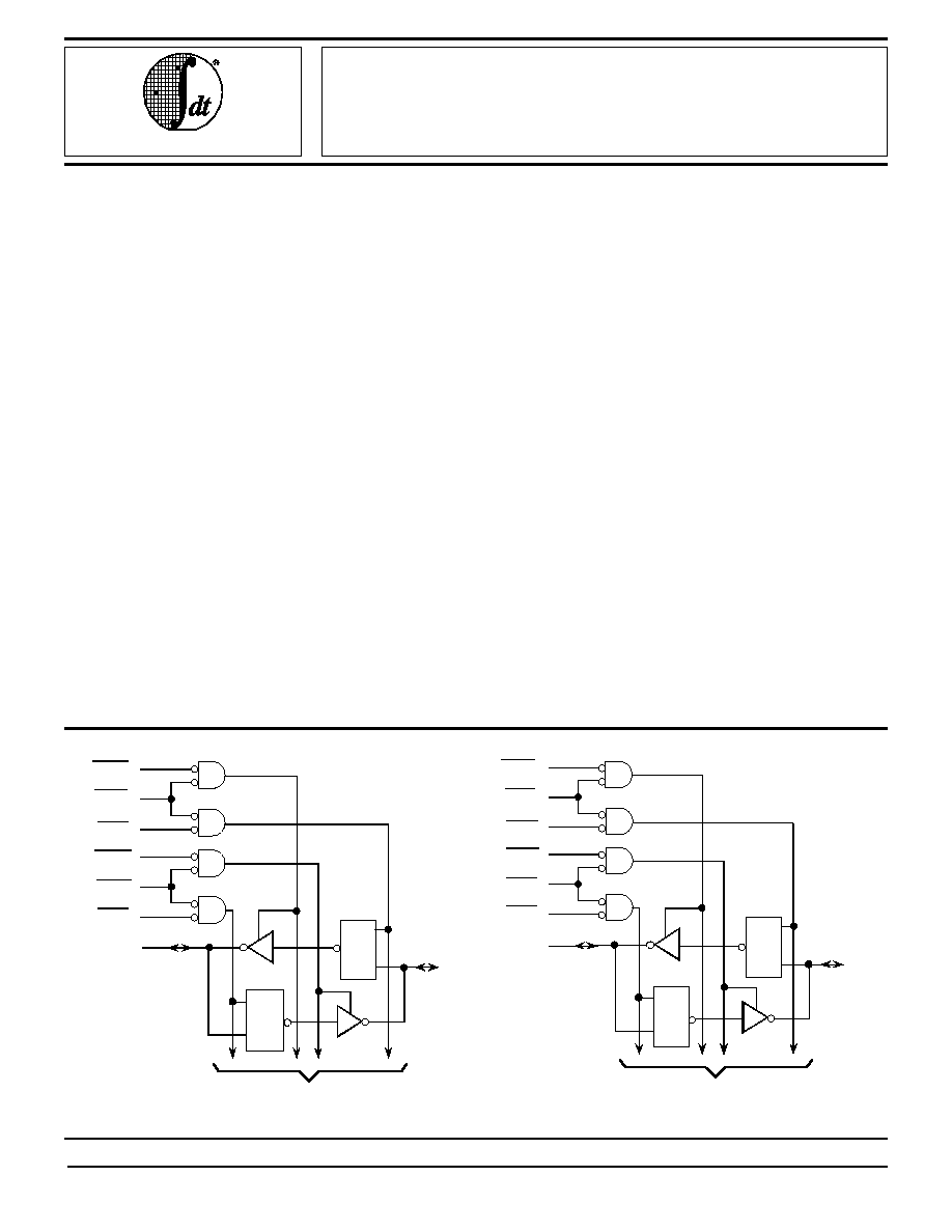
FUNCTIONAL BLOCK DIAGRAM
D
C
D
C
1
B
1
1
OEBA
1
CEBA
1
LEBA
1
OEAB
1
CEAB
1
A
1
1
LEAB
TO 7 OTHER CHANNELS
2618 drw 01
2
OEBA
2
CEBA
2
LEBA
D
C
2
OEAB
2
CEAB
2
A
1
2
B
1
2
LEAB
TO 7 OTHER CHANNELS
2618 drw 02
D
C
DESCRIPTION:
The FCT16543T/AT/CT/ET and FCT162543T/AT/CT/ET
16-bit latched transceivers are built using advanced dual metal
CMOS technology. These high-speed, low-power devices are
organized as two independent 8-bit D-type latched transceiv-
ers with separate input and output control to permit indepen-
dent control of data flow in either direction. For example, the A-
to-B Enable (x
CEAB
) must be LOW in order to enter data from
the A port or to output data from the B port. x
LEAB
controls the
latch function. When x
LEAB
is LOW, the latches are transpar-
ent. A subsequent LOW-to-HIGH transition of x
LEAB
signal
puts the A latches in the storage mode. x
OEAB
performs output
enable function on the B port. Data flow from the B port to the
A port is similar but requires using x
CEBA
, x
LEBA
, and x
OEBA
inputs. Flow-through organization of signal pins simplifies
layout. All inputs are designed with hysteresis for improved
noise margin.
The FCT16543T/AT/CT/ET are ideally suited for driving
high-capacitance loads and low-impedance backplanes. The
output buffers are designed with power off disable capability to
allow "live insertion" of boards when used as backplane drivers.
The FCT162543T/AT/CT/ET have balanced output drive
with current limiting resistors. This offers low ground bounce,
minimal undershoot, and controlled output fall times≠reducing
the need for external series terminating resistors. The
FCT162543T/AT/CT/ET are plug-in replacements for the
FCT16543T/AT/CT/ET and 54/74ABT16543 for on-board bus
interface applications.
5.12
2
IDT54/74FCT16543T/AT/CT/ET, 162543T/AT/CT/ET
FAST CMOS 16-BIT LATCHED TRANSCEIVER
MILITARY AND COMMERCIAL TEMPERATURE RANGES
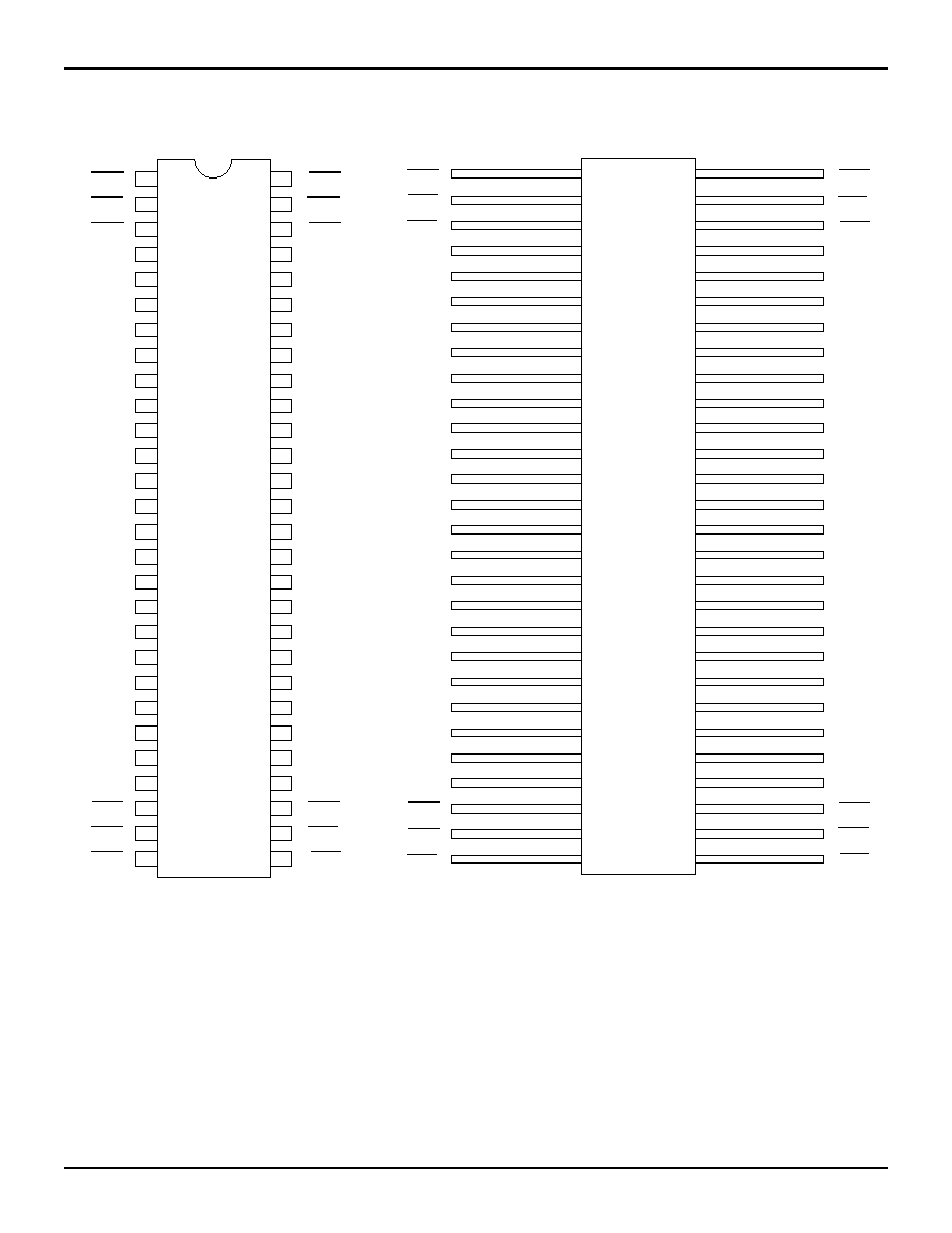
PIN CONFIGURATIONS
GND
1
A
1
1
A
2
V
CC
1
A
3
1
A
4
GND
1
A
5
1
A
6
1
A
7
1
A
8
GND
2
A
1
2
A
2
V
CC
2
A
3
2
A
5
2
A
4
2
A
7
GND
2
A
8
2
A
6
1
B
1
1
B
2
GND
1
B
3
1
B
4
V
CC
1
B
5
1
B
6
1
OEBA
1
B
7
1
B
8
2
B
1
2
B
2
GND
2
B
3
2
B
4
V
CC
2
B
5
GND
2
B
7
2
B
6
2
B
8
GND
2
OEBA
2
OEAB
2
LEAB
2
CEAB
1
OEAB
1
LEAB
1
CEAB
1
LEBA
1
CEBA
2
LEBA
2
CEBA
47
37
38
39
40
41
42
43
44
45
46
33
34
35
36
56
55
49
50
51
52
53
54
48
1
2
3
4
5
6
7
8
9
10
12
13
14
15
16
17
18
19
20
11
21
22
23
24
29
30
31
32
25
26
27
28
2618 drw 04
CERPACK
TOP VIEW
E56-1
1
B
1
1
B
2
GND
1
B
3
1
B
4
V
CC
1
B
5
1
B
6
1
OEBA
1
B
7
1
B
8
2
B
1
2
B
2
GND
2
B
3
2
B
4
V
CC
2
B
5
GND
2
B
7
2
B
6
2
B
8
GND
2
OEBA
GND
1
A
1
1
A
2
V
CC
1
A
3
1
A
4
GND
1
A
5
1
A
6
1
A
7
1
A
8
GND
2
A
1
2
A
2
V
CC
2
A
3
2
A
5
2
A
4
2
A
7
GND
2
A
8
2
A
6
2
OEAB
2
LEAB
2
CEAB
1
CEAB
1
LEAB
1
OEAB
1
LEBA
1
CEBA
2
LEBA
2
CEBA
2618 drw 03
47
37
38
39
40
41
42
43
44
45
46
33
34
35
36
56
55
49
50
51
52
53
54
48
1
2
3
4
5
6
7
8
9
10
12
13
14
15
16
17
18
19
20
11
21
22
23
24
SSOP/
TSSOP/TVSOP
TOP VIEW
SO56-1
SO56-2
SO56-3
29
30
31
32
25
26
27
28
IDT54/74FCT16543T/AT/CT/ET, 162543T/AT/CT/ET
FAST CMOS 16-BIT LATCHED TRANSCEIVER
MILITARY AND COMMERCIAL TEMPERATURE RANGES
5.12
3
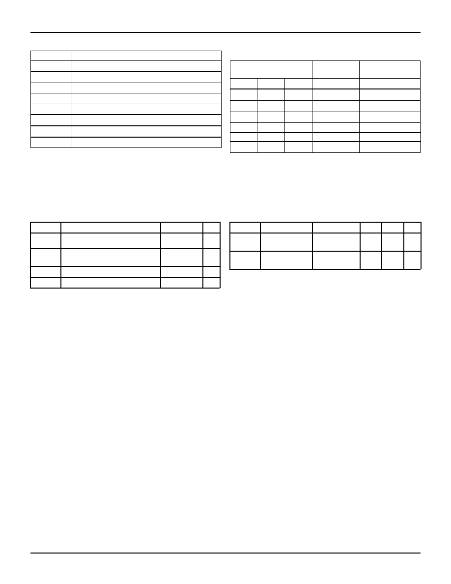
FUNCTION TABLE
(1, 2)
For A-to-B (Symmetric with B-to-A)
Latch
Output
Inputs
Status
Buffers
x
CEAB
CEAB
x
LEAB
LEAB
x
OEAB
OEAB
xAx to xBx
xBx
H
X
X
Storing
High Z
X
H
X
Storing
X
L
L
L
Transparent
Current A Inputs
L
H
L
Storing
Previous* A Inputs
L
L
H
Transparent
High Z
L
H
H
Storing
High Z
PIN DESCRIPTION
Pin Names
Description
x
OEAB
A-to-B Output Enable Input (Active LOW)
x
OEBA
B-to-A Output Enable Input (Active LOW)
x
CEAB
A-to-B Enable Input (Active LOW)
x
CEBA
B-to-A Enable Input (Active LOW)
x
LEAB
A-to-B Latch Enable Input (Active LOW)
x
LEBA
B-to-A Latch Enable Input (Active LOW)
xAx
A-to-B Data Inputs or B-to-A 3-State Outputs
xBx
B-to-A Data Inputs or A-to-B 3-State Outputs
2618 tbl 01
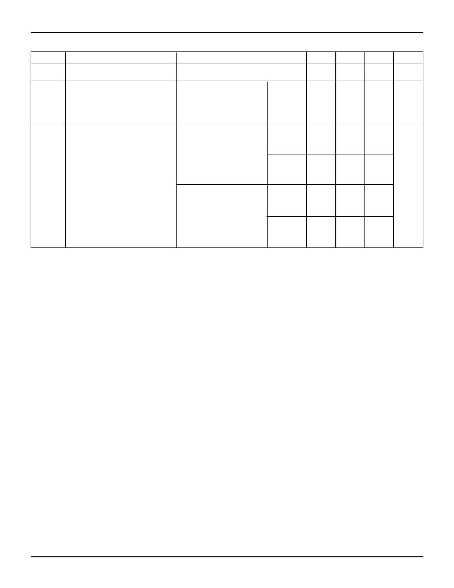
ABSOLUTE MAXIMUM RATINGS
(1)
Symbol
Description
Max.
Unit
V
TERM(2)
Terminal Voltage with Respect to
GND
≠0.5 to +7.0
V
V
TERM(3)
Terminal Voltage with Respect to
GND
≠0.5 to
V
CC
+0.5
V
T
STG
Storage Temperature
≠65 to +150
∞
C
I
OUT
DC Output Current
≠60 to +120 mA
2618 lnk 03
NOTES:
1. Stresses greater than those listed under ABSOLUTE MAXIMUM RAT-
INGS may cause permanent damage to the device. This is a stress rating
only and functional operation of the device at these or any other condi-
tions above those indicated in the operational sections of this specifica-
tion is not implied. Exposure to absolute maximum rating conditions for
extended periods may affect reliability.
2. All device terminals except FCT162XXXT Output and I/O terminals.
3. Output and I/O terminals for FCT162XXXT.
NOTES:
2618 tbl 02
1. * Before x
LEAB
LOW-to-HIGH Transition
H = HIGH Voltage Level
L = LOW Voltage Level
X = Don't Care
2. A-to-B data flow shown; B-to-A flow control is the same, except using
x
CEBA
, x
LEBA
and x
OEBA
.
NOTE:
1. This parameter is measured at characterization but not tested.
CAPACITANCE
(T
A
= +25
∞
C, f = 1.0MHz)
Symbol
Parameter
(1)
Conditions
Typ.
Max.
Unit
C
IN
Input
Capacitance
V
IN
= 0V
3.5
6.0
pF
C
I/O
I/O
Capacitance
V
OUT
= 0V
3.5
8.0
pF
2618 lnk 04
5.12
4
IDT54/74FCT16543T/AT/CT/ET, 162543T/AT/CT/ET
FAST CMOS 16-BIT LATCHED TRANSCEIVER
MILITARY AND COMMERCIAL TEMPERATURE RANGES
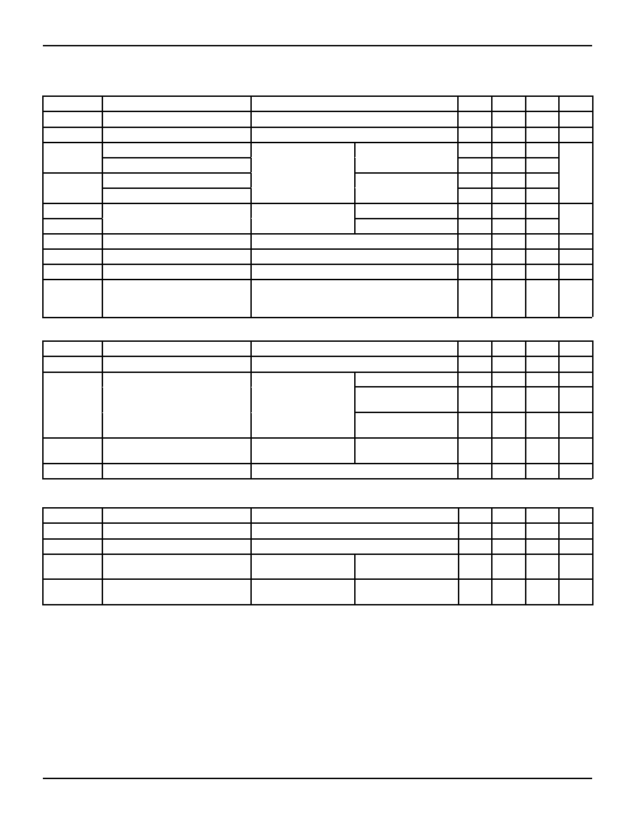
DC ELECTRICAL CHARACTERISTICS OVER OPERATING RANGE
Following Conditions Apply Unless Otherwise Specified:
Commercial: T
A
= ≠40
∞
C to +85
∞
C, V
CC
= 5.0V
±
10%; Military: T
A
= ≠55
∞
C to +125
∞
C, V
CC
= 5.0V
±
10%
OUTPUT DRIVE CHARACTERISTICS FOR FCT162543T
2618 lnk 06
NOTES:
1. For conditions shown as Max. or Min., use appropriate value specified under Electrical Characteristics for the applicable device type.
2. Typical values are at Vcc = 5.0V, +25
∞
C ambient.
3. Not more than one output should be tested at one time. Duration of the test should not exceed one second.
4. Duration of the condition can not exceed one second.
5. The test limit for this parameter is
±
5
µ
A at T
A
= ≠55
∞
C.
2618 lnk 07
Symbol
Parameter
Test Conditions
(1)
Min.
Typ.
(2)
Max.
Unit
I
ODL
Output LOW Current
V
CC
= 5V, V
IN
= V
IH
or
V
IL,
V
OUT
= 1.5V
(3)
60
115
200
mA
I
ODH
Output HIGH Current
V
CC
= 5V, V
IN
= V
IH
or V
IL,
V
OUT
= 1.5V
(3)
≠60
≠115
≠200
mA
V
OH
Output HIGH Voltage
V
CC
= Min.
V
IN
= V
IH
or V
IL
I
OH
= ≠16mA MIL.
I
OH
= ≠24mA COM'L.
2.4
3.3
--
V
V
OL
Output LOW Voltage
V
CC
= Min.
V
IN
= V
IH
or V
IL
I
OL
= 16mA MIL.
I
OL
= 24mA COM'L.
--
0.3
0.55
V
Symbol
Parameter
Test Conditions
(1)
Min.
Typ.
(2)
Max.
Unit
V
IH
Input HIGH Level
Guaranteed Logic HIGH Level
2.0
--
--
V
V
IL
Input LOW Level
Guaranteed Logic LOW Level
--
--
0.8
V
I
I H
Input HIGH Current (Input pins)
(5)
V
CC
= Max.
V
I
= V
CC
--
--
±
1
µ
A
Input HIGH Current (I/O pins)
(5)
--
--
±
1
I
I L
Input LOW Current (Input pins)
(5)
V
I
= GND
--
--
±
1
Input LOW Current (I/O pins)
(5)
--
--
±
1
I
OZH
High Impedance Output Current
V
CC
= Max.
V
O
= 2.7V
--
--
±
1
µ
A
I
OZL
(3-State Output pins)
(5)
V
O
= 0.5V
--
--
±
1
V
IK
Clamp Diode Voltage
V
CC
= Min., I
IN
= ≠18mA
--
≠
0.7
≠
1.2
V
I
OS
Short Circuit Current
V
CC
= Max., V
O
= GND
(3)
≠80
≠
140
≠
225
mA
V
H
Input Hysteresis
--
--
100
--
mV
I
CCL
I
CCH
I
CCZ
Quiescent Power Supply Current
V
CC
= Max., V
IN
= GND or V
CC
--
5
500
µ
A
2618 lnk 05
OUTPUT DRIVE CHARACTERISTICS FOR FCT16543T
Symbol
Parameter
Test Conditions
(1)
Min.
Typ.
(2)
Max.
Unit
I
O
Output Drive Current
V
CC
= Max., V
O
= 2.5V
(3)
≠50
--
≠
180
mA
V
OH
Output HIGH Voltage
V
CC
= Min.
I
OH
= ≠3mA
2.5
3.5
--
V
V
IN
= V
IH
or V
IL
I
OH
= ≠12mA MIL.
I
OH
= ≠15mA COM'L.
2.4
3.5
--
V
I
OH
= ≠24mA MIL.
I
OH
= ≠32mA COM'L.
(4)
2.0
3.0
--
V
V
OL
Output LOW Voltage
V
CC
= Min.
V
IN
= V
IH
or V
IL
I
OL
= 48mA MIL.
I
OL
= 64mA COM'L.
--
0.2
0.55
V
I
OFF
Input/Output Power Off Leakage
(5)
V
CC
= 0V, V
IN
or V
O
4.5V
--
--
±
1
µ
A
IDT54/74FCT16543T/AT/CT/ET, 162543T/AT/CT/ET
FAST CMOS 16-BIT LATCHED TRANSCEIVER
MILITARY AND COMMERCIAL TEMPERATURE RANGES
5.12
5
NOTES:
1. For conditions shown as Max. or Min., use appropriate value specified under Electrical Characteristics for the applicable device type.
2. Typical values are at V
CC
= 5.0V, +25
∞
C ambient.
3. Per TTL driven input (V
IN
= 3.4V). All other inputs at V
CC
or GND.
4. This parameter is not directly testable, but is derived for use in Total Power Supply Calculations.
5. Values for these conditions are examples of the I
CC
formula. These limits are guaranteed but not tested.
6. I
C
= I
QUIESCENT
+ I
INPUTS
+ I
DYNAMIC
I
C
= I
CC
+
I
CC
D
H
N
T
+ I
CCD
(f
CP
N
CP
/2 + f
i
N
i
)
I
CC
= Quiescent Current (I
CCL
,
I
CCH
and I
CCZ
)
I
CC
= Power Supply Current for a TTL High Input (V
IN
= 3.4V)
D
H
= Duty Cycle for TTL Inputs High
N
T
= Number of TTL Inputs at D
H
I
CCD
= Dynamic Current Caused by an Input Transition Pair (HLH or LHL)
f
CP
= Clock Frequency for Register Devices (Zero for Non-Register Devices)
N
CP
= Number of Clock Inputs at f
CP
f
i
= Input Frequency
N
i
= Number of Inputs at f
i
2618 tbl 08
POWER SUPPLY CHARACTERISTICS
Symbol
Parameter
Test Conditions
(1)
Min.
Typ.
(2)
Max.
Unit
I
CC
Quiescent Power Supply
V
CC
= Max.
--
0.5
1.5
mA
Current TTL Inputs HIGH
V
IN
= 3.4V
(3)
I
CCD
Dynamic Power Supply Current
(4)
V
CC
= Max., Outputs Open
V
IN
= V
CC
--
60
100
µ
A/
x
CEAB
and x
OEAB
= GND
V
IN
= GND
MHz
x
CEBA
= V
CC
One Input Toggling
50% Duty Cycle
I
C
Total Power Supply Current
(6)
V
CC
= Max., Outputs Open
V
IN
= V
CC
--
0.6
1.5
mA
f
i
= 10MHz
V
IN
= GND
50% Duty Cycle
x
LEAB
, x
CEAB
and
x
OEAB
= GND
V
IN
= 3.4V
--
0.9
2.3
x
CEBA
= V
CC
V
IN
= GND
One Bit Toggling
V
CC
= Max., Outputs Open
V
IN
= V
CC
--
2.4
4.5
(5)
f
i
= 2.5MHz
V
IN
= GND
50% Duty Cycle
x
LEAB
, x
CEAB
and
x
OEAB
= GND
V
IN
= 3.4V
--
6.4
16.5
(5)
x
CEBA
= V
CC
V
IN
= GND
Sixteen Bits Toggling