166244T
1
IDT54/74FCT166244T/AT/CT
FAST CMOS 16-BIT BUFFER/LINE DRIVER
MILITARY AND COMMERCIAL TEMPERATURE RANGES
AUGUST 1999
1999 Integrated Device Technology, Inc.
DSC-5462/-
c
IDT54/74FCT166244T/AT/CT
MILITARY AND COMMERCIAL TEMPERATURE RANGES
FAST CMOS 16-BIT
BUFFER/LINE DRIVER
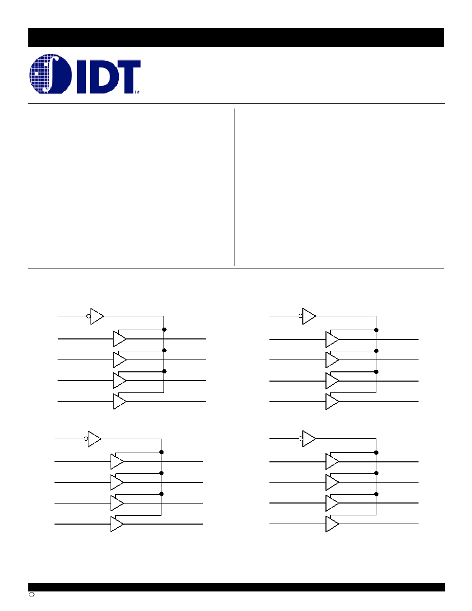
DESCRIPTION:
The 16-Bit Buffer/Line Driver is for bus interface or signal buffering
applications requiring high speed and low power dissipation. These devices
have a flow through pin organization, and shrink packaging to simplify board
layout. All inputs are designed with hysteresis for improved noise margin. The
three-state controls allow independent 4-bit, 8-bit or combined 16-bit operation.
These parts are plug in replacements for 54/74ABT16244 where higher
speed, lower noise or lower power dissipation levels are desired.
The FCT166244T/AT/CT are suited for very low noise, point-to-point
driving where there is a single receiver, or a very light lumped load
(<100pF). The buffers are designed to limit the output current to levels which
will avoid noise and ringing on the signal lines without using external series
terminating resistors.
FUNCTIONAL BLOCK DIAGRAM
3
OE
3
A
1
3
A
2
3
A
3
3
A
4
3
Y
1
3
Y
2
3
Y
3
3
Y
4
1
Y
1
1
Y
2
1
Y
3
1
Y
4
1
A
1
1
A
2
1
A
3
1
A
4
1
OE
4
OE
4
A
1
4
A
2
4
A
3
4
A
4
4
Y
1
4
Y
2
4
Y
3
4
Y
4
2
OE
2
A
1
2
A
2
2
A
3
2
A
4
2
Y
1
2
Y
2
2
Y
3
2
Y
4
FEATURES:
-
0.5 MICRON CMOS Technology
-
High-speed, low-power CMOS replacement for ABT functions
-
Typical t
SK
(o) (Output Skew) < 250ps
-
Low input and output leakage
1� A (max.)
-
ESD > 2000V per MIL-STD-883, Method 3015; > 200V using
machine model (C = 200pF, R = 0)
-
25 mil pitch SSOP, 19.6 mil pitch TSSOP, 15.7 mil pitch TVSOP
and 25 mil pitch CERPACK packages
-
Extended commercial range of -40�C to +85�C
-
Light Drive Balanced Output:
�
�8mA (commercial)
�
�6mA (military)
-
Minimal system switching noise
-
Typical V
OLP
(Output Ground Bounce) < 0.25V at V
CC
= 5V,T
A
=
25�C
2
MILITARY AND COMMERCIAL TEMPERATURE RANGES
IDT54/74FCT166244T/AT/CT
FAST CMOS 16-BIT BUFFER/LINE DRIVER
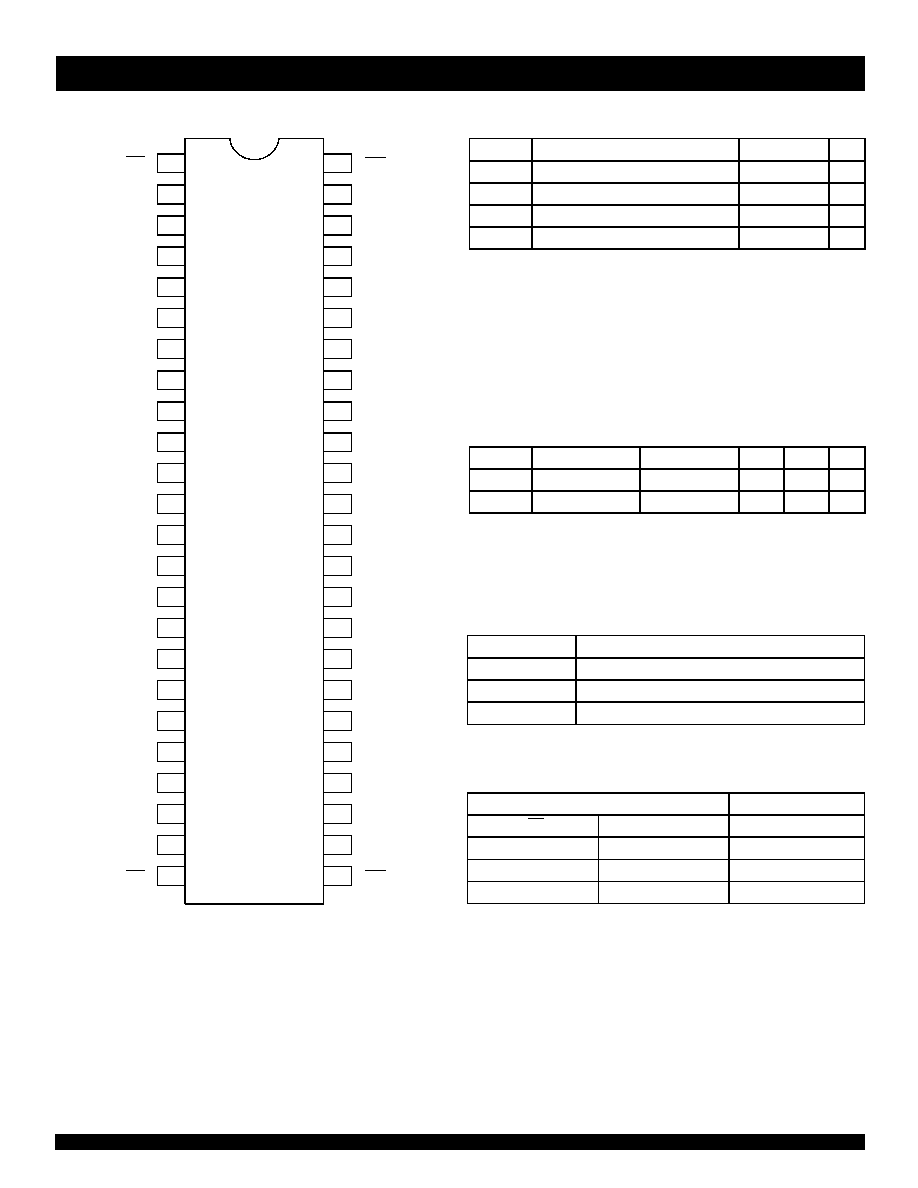
SSOP/ TSSOP/ TVSOP/ CERPACK
TOP VIEW
PIN CONFIGURATION
ABSOLUTE MAXIMUM RATINGS
(1)
Symbol
Description
Max
Unit
V
TERM(2)
Terminal Voltage with Respect to GND
�0.5 to +7
V
V
TERM(3)
Terminal Voltage with Respect to GND
�0.5 to V
CC
+0.5
V
T
STG
Storage Temperature
�65 to +150
�C
I
OUT
DC Output Current
�60 to +120
mA
5v16-link
NOTES:
1. Stresses greater than those listed under ABSOLUTE MAXIMUM
RATINGS may cause permanent damage to the device. This is a
stress rating only and functional operation of the device at these or
any other conditions above those indicated in the operational sections
of this specification is not implied. Exposure to absolute maximum
rating conditions for extended periods may affect reliability.
2. All device
terminals except FCT162XXXT Output and I/O terminals.
3. Output and I/O terminals for FCT162XXXT.
CAPACITANCE (T
A
= +25
O
C, f = 1.0MHz)
Symbol
Parameter
(1)
Conditions
Typ.
Max.
Unit
C
IN
Input Capacitance
V
IN
= 0V
3.5
6
pF
C
OUT
Output Capacitance
V
OUT
= 0V
3.5
8
pF
5v16-link
NOTE:
1. This parameter is measured at characterization but not tested.
1
Y
1
G ND
1
Y
3
V
C C
G ND
3
Y
2
G ND
V
C C
G ND
1
Y
2
1
Y
4
2
Y
1
2
Y
2
2
Y
3
2
Y
4
3
Y
1
3
Y
3
3
Y
4
4
Y
1
4
Y
3
4
Y
4
4
Y
2
4
O E
1
A
1
1
A
2
G ND
1
A
3
1
A
4
V
C C
2
A
1
2
A
2
2
A
3
2
A
4
3
A
1
3
A
2
3
A
3
3
A
4
V
C C
4
A
1
4
A
3
4
A
4
4
A
2
G ND
G ND
G ND
2
O E
3
O E
39
29
30
31
32
33
34
35
36
37
38
25
26
27
28
48
47
41
42
43
44
45
46
40
1
2
3
4
5
6
7
8
9
10
12
13
14
15
16
17
18
19
20
11
21
22
23
24
SO48-1
SO48-2
SO48-3
E48-1
1
O E
NOTE:
1. H = HIGH Voltage Level
X = Don't Care
L = LOW Voltage Level
Z = High-Impedance
3. Output and I/O terminals for FCT162XXXT and FCT166XXXT.
PIN DESCRIPTION
Pin Names
Description
x
OE
3�State Output Enable Inputs (Active LOW)
xAx
Data Inputs
xYx
3-State Outputs
FUNCTION TABLE
(1)
Inputs
Outputs
xOE
xAx
xYx
L
L
L
L
H
H
H
X
Z
3
IDT54/74FCT166244T/AT/CT
FAST CMOS 16-BIT BUFFER/LINE DRIVER
MILITARY AND COMMERCIAL TEMPERATURE RANGES
DC ELECTRICAL CHARACTERISTICS OVER OPERATING RANGE
Following Conditions Apply Unless Otherwise Specified:
Commercial: T
A
= -40�C to +85�C, V
CC
= 5.0V �10%; Military: T
A
= -55�C to +125�C, V
CC
= 5.0V �10%
Symbol
Parameter
Test Conditions
(1)
Min.
Typ.
(2)
Max.
Unit
V
IH
Input HIGH Level
Guaranteed Logic HIGH Level
2
--
--
V
V
IL
Input LOW Level
Guaranteed Logic LOW Level
--
--
0.8
V
I
IH
Input HIGH Current (Input pins)
(5)
V
CC
= Max.
V
I
= V
CC
--
--
�
1
� A
Input HIGH Current (I/O pins)
(5)
--
--
�
1
I
IL
Input LOW Current (Input pins)
(5)
V
I
= GND
--
--
�
1
Input LOW Current (I/O pins)
(5)
--
--
�
1
I
OZH
High Impedance Output Current
V
CC
= Max.
V
O
= 2.7V
--
--
�
1
� A
I
OZL
(3-State Output pins)
(5)
V
O
= 0.5V
--
--
�
1
V
IK
Clamp Diode Voltage
V
CC
= Min., I
IN
= �18mA
--
�0.7
�1.2
V
I
OS
Short Circuit Current
V
CC
= Max., V
O
= GND
(3)
�80
�140
�250
mA
V
H
Input Hysteresis
--
--
100
--
mV
I
CCL
I
CCH
I
CCZ
Quiescent Power Supply Current
V
CC
= Max.
V
IN
= GND or V
CC
--
5
500
� A
5v16-link
OUTPUT DRIVE CHARACTERISTICS
Symbol
Parameter
Test Conditions
(1)
Min.
Typ.
(2)
Max.
Unit
I
ODL
Output LOW Current
V
CC
= 5V, V
IN
= V
IH
or V
IL
, V
O
= 1.5V
(3)
16
48
96
mA
I
ODH
Output HIGH Current
V
CC
= 5V, V
IN
= V
IH
or V
IL
, V
O
= 1.5V
(3)
�16
�48
�96
mA
V
OH
Output HIGH Voltage
V
CC
= Min.
I
OH
= �6mA MIL
2.4
3.3
--
V
V
IN
= V
IH
or V
IL
I
OH
= �8mA COM'L
V
OL
Output LOW Voltage
V
CC
= Min.
I
OL
= 6mA MIL
--
0.3
0.55
V
V
IN
= V
IH
or V
IL
I
OL
= 8mA COM'L
NOTES:
1. For conditions shown as Max. or Min., use appropriate value specified under Electrical Characteristics for the applicable device type.
2. Typical values are at V
CC
= 5.0V, +25�C ambient.
3. Not more than one output should be shorted at one time. Duration of the test should not exceed one second.
4. Duration of the condition can not exceed one second.
5. The test limit for this parameter is �5�A at T
A
= -55�C.
4
MILITARY AND COMMERCIAL TEMPERATURE RANGES
IDT54/74FCT166244T/AT/CT
FAST CMOS 16-BIT BUFFER/LINE DRIVER
NOTES:
1. For conditions shown as Max. or Min., use appropriate value specified under Electrical Characteristics for the applicable device type.
2. Typical values are at V
CC
= 5.0V, +25�C ambient.
3. Per TTL driven input (V
IN
= 3.4V). All other inputs at V
CC
or GND.
4. This parameter is not directly testable, but is derived for use in Total Power Supply Calculations.
5. Values for these conditions are examples of the I
CC
formula. These limits are guaranteed but not tested.
6. I
C
= I
QUIESCENT
+ I
INPUTS
+ I
DYNAMIC
I
C
= I
CC
+
I
CC
D
H
N
T
+ I
CCD
(f
CP
N
CP
/2 + fiNi)
I
CC
= Quiescent Current (I
CCL
, I
CCH
and I
CCZ
)
I
CC
= Power Supply Current for a TTL High Input (V
IN
= 3.4V)
D
H
= Duty Cycle for TTL Inputs High
N
T
= Number of TTL Inputs at D
H
I
CCD
= Dynamic Current Caused by an Input Transition Pair (HLH or LHL)
f
CP
= Clock Frequency for Register Devices (Zero for Non-Register Devices)
N
CP
= Number of Clock Inputs at f
CP
fi = Input Frequency
Ni = Number of Inputs at fi
POWER SUPPLY CHARACTERISTICS
Symbol
Parameter
Test Conditions
(1)
Min.
Typ.
(2)
Max.
Unit
I
CC
Quiescent Power Supply Current
TTL Inputs HIGH
V
CC
= Max.
V
IN
= 3.4V
(3)
--
0.5
1.5
mA
I
CCD
Dynamic Power Supply Current
(4)
V
CC
= Max.
Outputs Open
x
OE = GND
One Input Toggling
50% Duty Cycle
V
IN
= V
CC
V
IN
= GND
--
60
100
� A/
MHz
I
C
Total Power Supply Current
(6)
V
CC
= Max.
Outputs Open
fi = 10MHz
V
IN
= V
CC
V
IN
= GND
--
0.6
1.5
mA
50% Duty Cycle
x
OE = GND
One Bit Toggling
V
IN
= 3.4V
V
IN
= GND
--
0.9
2.3
V
CC
= Max.
Outputs Open
fi = 2.5MHz
V
IN
= V
CC
V
IN
= GND
--
2.4
4.5
(5)
50% Duty Cycle
x
OE = GND
Sixteen Bits Toggling
V
IN
= 3.4V
V
IN
= GND
--
6.4
16.5
(5)
5
IDT54/74FCT166244T/AT/CT
FAST CMOS 16-BIT BUFFER/LINE DRIVER
MILITARY AND COMMERCIAL TEMPERATURE RANGES
NOTES:
1. See test circuit and waveforms.
2. Minimum limits are guaranteed but not tested on Propagation Delays.
3. Skew between any two outputs of the same package switching in the same direction. This parameter is guaranteed by design.
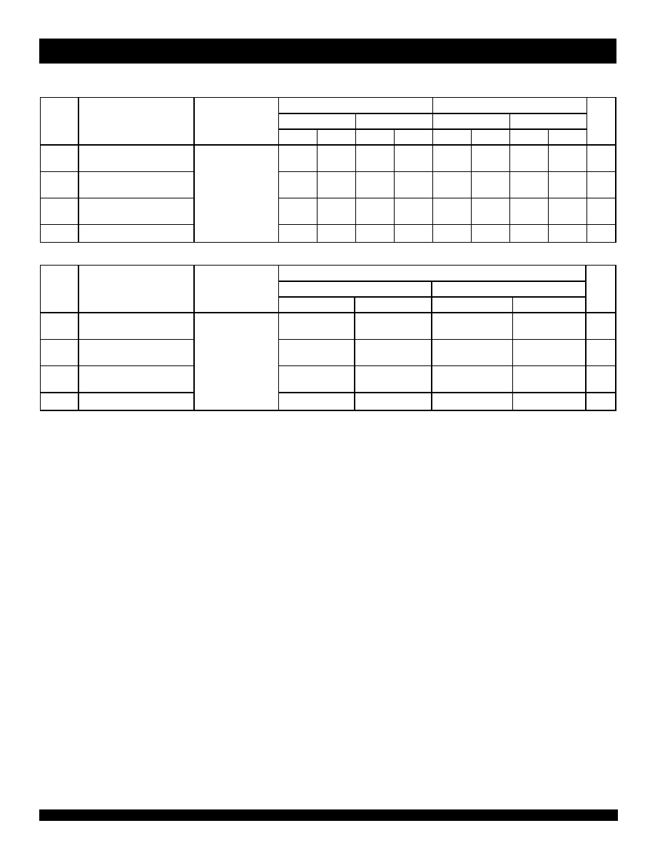
SWITCHING CHARACTERISTICS OVER OPERATING RANGE
FCT166244T
FCT166244AT
Com'l.
Mil.
Com'l.
Mil.
Symbol
Parameter
Condition
(1)
Min
.
(2)
Max
.
Min
.
(2)
Max
.
Min
.
(2)
Max
.
Min
.
(2)
Max
.
Unit
t
PLH
t
PHL
Propagation Delay
xAx to xYx
C
L
= 50pF
R
L
= 500
1.5
6.5
1.5
7
1.5
4.8
1.5
5.1
ns
t
PZH
t
PZL
Output Enable Time
1.5
8
1.5
8.5
1.5
6.2
1.5
6.5
ns
t
PHZ
t
PLZ
Output Disable Time
1.5
7
1.5
7.5
1.5
5.6
1.5
5.9
ns
t
SK
(o)
Output Skew
(3)
--
0.5
--
0.5
--
0.5
--
0.5
ns
FCT166244CT
Com'l.
Mil.
Symbol
Parameter
Condition
(1)
Min
.
(2)
Max
.
Min
.
(2)
Max
.
Unit
t
PLH
t
PHL
Propagation Delay
xAx to xYx
C
L
= 50pF
R
L
= 500
1.5
4.1
1.5
4.6
ns
t
PZH
t
PZL
Output Enable Time
1.5
5.8
1.5
6.5
ns
t
PHZ
t
PLZ
Output Disable Time
1.5
5.2
1.5
5.7
ns
t
SK
(o)
Output Skew
(3)
--
0.5
--
0.5
ns