Integrated Device Technology, Inc.
MILITARY AND COMMERCIAL TEMPERATURE RANGES
MAY 1992
©
1992 Integrated Device Technology, Inc.
7.9
DSC-4201/3
Æ
The IDT logo is a registered trademark of Integrated Device Technology, Inc.
FAST is a registered trademark of National Semiconductor Co.
DIP/SOIC/CERPACK
TOP VIEW
FAST CMOS OCTAL
BIDIRECTIONAL
TRANSCEIVERS
IDT54/74FCT245/A/C
IDT54/74FCT640/A/C
IDT54/74FCT645/A/C
FEATURES:
∑ IDT54/74FCT245/640/645 equivalent to FAST
TM
speed
and drive
∑ IDT54/74FCT245A/640A/645A 25% faster than FAST
∑ IDT54/74FCT245C/640C/645C 40% faster than FAST
∑ TTL input and output level compatible
∑ CMOS output level compatible
∑ I
OL
= 64mA (commercial) and 48mA (military)
∑ Input current levels only 5
µ
A max.
∑ CMOS power levels (2.5mW typical static)
∑ Direction control and over-riding 3-state control
∑ Product available in Radiation Tolerant and Radiation
Enhanced versions
∑ Military product compliant to MIL-STD-883, Class B and
DESC listed
∑ Meets or exceeds JEDEC Standard 18 specifications
DESCRIPTION:
The IDT octal bidirectional transceivers are built using an
advanced dual metal CMOS technology. The IDT54/
74FCT245/A/C, IDT54/74FCT640/A/C and IDT54/74FCT645/
A/C are designed for asynchronous two-way communication
between data buses. The transmit/receive (T/
R
) input deter-
mines the direction of data flow through the bidirectional
transceiver. Transmit (active HIGH) enables data from A
ports to B ports, and receive (active LOW) from B ports to A
ports. The output enable (
OE
) input, when HIGH, disables
both A and B ports by placing them in High-Z condition.
The IDT54/74FCT245/A/C and IDT54/74FCT645/A/C
transceivers have non-inverting outputs. The IDT54/
74FCT640/A/C has inverting outputs.
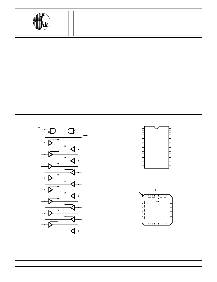
FUNCTIONAL BLOCK DIAGRAM
PIN CONFIGURATIONS
2534 drw 02
A
B
0
0
T/R
OE
A
B
1
1
A
B
2
2
A
B
3
3
A
B
4
4
A
B
5
5
A
B
6
6
A
B
7
7
5
6
7
8
9
10
A
1
A
2
A
3
1
2
3
4
20
19
18
17
16
15
14
13
Vcc
12
11
T/R
B
1
A
4
A
5
A
6
A
7
OE
B
2
B
3
B
4
B
5
B
6
GND
B
7
A
0
B
0
P20-1
D20-1
SO20-2
&
E20-1
2534 drw 01
INDEX
B
0
B
1
B
2
B
3
B
4
A
2
A
3
A
4
A
5
A
6
B
7
B
6
B
GND
A
7
A
0
A
1
Vcc
T/R
OE
15
14
5
18
17
16
5
6
7
8
9
10 11 12
1
4
3
2
20
13
19
L20-2
LCC
TOP VIEW
NOTES:
1. FCT245, 645 are noninverting options.
2. FCT640 is the inverting option.
1
7.9
2
IDT54/74FCT245/A/C, IDT54/74FCT640/A/C, IDT54/74FCT645/A/C
FAST CMOS OCTAL BIDIRECTIONAL TRANSCEIVERS
MILITARY AND COMMERCIAL TEMPERATURE RANGES
PIN DESCRIPTION
Pin Names
Description
OE
Output Enable Input (Active LOW)
T/
R
Transmit/Receive Input
A
0
≠A
7
Side A Inputs or 3-State Outputs
B
0
≠B
7
Side B Inputs or 3-State Outputs
2534 tbl 05
FUNCTION TABLE
(2)
Inputs
OE
OE
T/
R
R
Outputs
L
L
Bus B Data to Bus A
(1)
L
H
Bus A Data to Bus B
(1)
H
X
High Z State
NOTES:
2534 tbl 06
1. 640 is inverting from input to output.
2. H = HIGH Voltage Level
L = LOW Voltage Level
X = Don't Care
ABSOLUTE MAXIMUM RATINGS
(1)
Symbol
Rating
Commercial
Military
Unit
V
TERM
(2)
Terminal Voltage
≠0.5 to +7.0
≠0.5 to +7.0
V
with Respect
to GND
V
TERM
(3)
Terminal Voltage
≠0.5 to V
CC
≠0.5 to V
CC
V
with Respect
to GND
T
A
Operating
0 to +70
≠55 to +125
∞
C
Temperature
T
BIAS
Temperature
≠55 to +125
≠65 to +135
∞
C
Under Bias
T
STG
Storage
≠55 to +125
≠65 to +150
∞
C
Temperature
P
T
Power Dissipation
0.5
0.5
W
I
OUT
DC Output Current
120
120
mA
NOTES:
2534 tbl 01
1. Stresses greater than those listed under ABSOLUTE MAXIMUM
RATINGS may cause permanent damage to the device. This is a stress
rating only and functional operation of the device at these or any other
conditions above those indicated in the operational sections of this
specification is not implied. Exposure to absolute maximum rating
conditions for extended periods may affect reliability. No terminal voltage
may exceed V
CC
by +0.5V unless otherwise noted.
2. Inputs and V
CC
terminals.
3. Outputs and I/O terminals.
CAPACITANCE
(T
A
= +25
∞
C, f = 1.0MHz)
Symbol
Parameter
(1)
Conditions
Typ. Max. Unit
C
IN
Input Capacitance
V
IN
= 0V
6
10
pF
C
I/O
I/O Capacitance
V
OUT
= 0V
8
12
pF
NOTE:
2534 tbl 02
1. This parameter is measured at characterization but not tested.
7.9
3
IDT54/74FCT245/A/C, IDT54/74FCT640/A/C, IDT54/74FCT645/A/C
FAST CMOS OCTAL BIDIRECTIONAL TRANSCEIVERS
MILITARY AND COMMERCIAL TEMPERATURE RANGES
DC ELECTRICAL CHARACTERISTICS OVER OPERATING RANGE
Following Conditions Apply Unless Otherwise Specified: V
LC
= 0.2V; V
HC
= V
CC
≠ 0.2V
Commercial: T
A
= 0
∞
C to +70
∞
C, V
CC
= 5.0V
±
5%; Military: T
A
= ≠55
∞
C to +125
∞
C, V
CC
= 5.0V
±
10%
Symbol
Parameter
Test Conditions
(1)
Min.
Typ.
(2)
Max.
Unit
V
IH
Input HIGH Level
Guaranteed Logic HIGH Level
2.0
--
--
V
V
IL
Input LOW Level
Guaranteed Logic LOW Level
--
--
0.8
V
I
IH
Input HIGH Current
V
CC
= Max
V
I
= V
CC
--
--
5
µ
A
(Except I/O pins)
V
I
= 2.7V
--
--
5
(4)
I
IL
Input LOW Current
V
I
= 0.5V
--
--
≠5
(4)
(Except I/O pins)
V
I
= GND
--
--
≠5
I
IH
Input HIGH Current
V
CC
= Max
V
I
= V
CC
--
--
15
µ
A
(I/O pins only)
V
I
= 2.7V
--
--
15
(4)
I
IL
Input LOW Current
V
I
= 0.5V
--
--
≠15
(4)
(I/O pins only)
V
I
= GND
--
--
≠15
V
IK
Clamp Diode Voltage
V
CC
= Min., I
N
= ≠18mA
--
≠0.7
≠1.2
V
I
OS
Short Circuit Current
V
CC
= Max.
(3)
, V
O
= GND
≠60
≠120
--
mA
V
OH
Output HIGH Voltage
V
CC
= 3V, V
IN
= V
LC
or V
HC
, I
OH
= ≠32
µ
A
V
HC
V
CC
--
V
V
CC
= Min.
I
OH
= ≠300
µ
A
V
HC
V
CC
--
V
IN
= V
IH
or V
IL
I
OH
= ≠12mA MIL.
2.4
4.3
--
I
OH
= ≠15mA COM'L.
2.4
4.3
--
V
OL
Output LOW Voltage
V
CC
= 3V, V
IN
= V
LC
or V
HC
, I
OL
= 300
µ
A
--
GND
V
LC
V
(Port A and Port B)
V
CC
= Min.
I
OL
= 300
µ
A
--
GND
V
LC
(4)
V
IN
= V
IH
or V
IL
I
OL
= 48mA MIL.
--
0.3
0.55
I
OL
= 64mA COM'L.
--
0.3
0.55
NOTES:
2534 tbl 03
1. For conditions shown as Max. or Min., use appropriate value specified under Electrical Characteristics for the applicable device type.
2. Typical values are at V
CC
= 5.0V, +25
∞
C ambient and maximum loading.
3. Not more than one output should be shorted at one time. Duration of the short circuit test should not exceed one second.
4. This parameter is guaranteed but not tested.

7.9
4
IDT54/74FCT245/A/C, IDT54/74FCT640/A/C, IDT54/74FCT645/A/C
FAST CMOS OCTAL BIDIRECTIONAL TRANSCEIVERS
MILITARY AND COMMERCIAL TEMPERATURE RANGES
POWER SUPPLY CHARACTERISTICS
V
LC
= 0.2V; V
HC
= V
CC
≠ 0.2V
Symbol
Parameter
Test Conditions
(1)
Min.
Typ.
(2)
Max.
Unit
I
CC
Quiescent Power Supply Current
Vcc = Max.
--
0.5
1.5
mA
V
IN
V
HC
; V
IN
V
LC
I
CC
Quiescent Power Supply Current
Vcc = Max.
--
0.5
2.0
mA
TTL Inputs HIGH
V
IN
= 3.4V
(3)
I
CCD
Dynamic Power Supply Current
(4)
Vcc = Max.
V
IN
V
HC
--
0.15
0.25
mA/MHz
Outputs Open
V
IN
V
LC
OE
= GND
T/
R
= GND or V
CC
One Input Toggling
50% Duty Cycle
I
C
Total Power Supply Current
(6)
Vcc = Max.
V
IN
V
HC
--
2.0
4.0
mA
Outputs Open
V
IN
V
LC
f
i
= 10MHz
(FCT)
50% Duty Cycle
V
IN
= 3.4V
--
2.3
5.0
T/
R
=
OE
= GND
V
IN
= GND
One Bit Toggling
Vcc = Max.
V
IN
V
HC
--
3.5
6.5
(5)
Outputs Open
V
IN
V
LC
f
i
= 2.5MHz
(FCT)
50% Duty Cycle
V
IN
= 3.4V
--
5.5
14.5
(5)
T/
R
=
OE
= GND
V
IN
= GND
Eight Bits Toggling
NOTES:
2534 tbl 04
1. For conditions shown as Max. or Min., use appropriate value specified under Electrical Characteristics for the applicable device type.
2. Typical values are at V
CC
= 5.0V, +25
∞
C ambient.
3. Per TTL driven input (V
IN
= 3.4V); all other inputs at V
CC
or GND.
4. This parameter is not directly testable, but is derived for use in Total Power Supply calculations.
5. Values for these conditions are examples of the I
CC
formula. These limits are guaranteed but not tested.
6. I
C
= I
QUIESCENT
+ I
INPUTS
+ I
DYNAMIC
I
C
= I
CC
+
I
CC
D
H
N
T
+ I
CCD
(f
CP
/2 + f
i
N
i
)
I
CC
= Quiescent Current
I
CC
= Power Supply Current for a TTL High Input (V
IN
= 3.4V)
D
H
= Duty Cycle for TTL Inputs High
N
T
= Number of TTL Inputs at D
H
I
CCD
= Dynamic Current Caused by an Output Transition Pair (HLH or LHL)
f
CP
= Clock Frequency for Register Devices (Zero for Non-Register Devices)
f
i
= Input Frequency
N
i
= Number of Inputs at f
i
All currents are in milliamps and all frequencies are in megahertz.
7.9
5
IDT54/74FCT245/A/C, IDT54/74FCT640/A/C, IDT54/74FCT645/A/C
FAST CMOS OCTAL BIDIRECTIONAL TRANSCEIVERS
MILITARY AND COMMERCIAL TEMPERATURE RANGES
t
PLH
Propagation Delay
C
L
= 50 pF
1.5
7.0
1.5
7.5
1.5
4.6
1.5
4.9
1.5
4.1
1.5
4.5
ns
t
PHL
A to B, B to A
R
L
= 500
t
PZH
Output Enable Time
1.5
9.5
1.5
10.0
1.5
6.2
1.5
6.5
1.5
5.8
1.5
6.2
ns
t
PZL
OE
to A or B
t
PHZ
Output Disable Time
1.5
7.5
1.5
10.0
1.5
5.0
1.5
6.0
1.5
4.8
1.5
5.2
ns
t
PLZ
OE
to A or B
t
PZH
Output EnableTime
1.5
9.5
1.5
10.0
1.5
6.2
1.5
6.5
1.5
5.8
1.5
6.2
ns
t
PZL
T/
R
to A or B
(3)
t
PHZ
Output Disable Time
1.5
7.5
1.5
10.0
1.5
5.0
1.5
6.0
1.5
4.8
1.5
5.2
ns
t
PLZ
T/
R
to A or B
(3)
2534 tbl 07
SWITCHING CHARACTERISTICS OVER OPERATING RANGE FOR FCT245/A/C
54/74FCT245
54/74FCT245A
54/74FCT245C
Com'l.
Mil.
Com'l.
Mil.
Com'l.
Mil.
Symbol
Parameter
Condition
(1)
Min.
(2)
Max. Min.
(2)
Max. Min.
(2)
Max. Min.
(2)
Max.
Min.
(2)
Max. Min
.
(2)
Max.
Unit
t
PLH
Propagation Delay
C
L
= 50 pF
2.0
7.0
2.0
8.0
1.5
5.0
1.5
5.3
1.5
4.4
1.5
4.7
ns
t
PHL
A to B, B to A
R
L
= 500
t
PZH
Output Enable Time
2.0
13.0
2.0
16.0
1.5
6.2
1.5
6.5
1.5
5.8
1.5
6.2
ns
t
PZL
OE
to A or B
t
PHZ
Output Disable Time
2.0
10.0
2.0
12.0
1.5
5.0
1.5
6.0
1.5
4.8
1.5
5.2
ns
t
PLZ
OE
to A or B
t
PZH
Output Enable Time
2.0
13.0
2.0
16.0
1.5
6.2
1.5
6.5
1.5
5.8
1.5
6.2
ns
t
PZL
T/
R
to A or B
(3)
t
PHZ
Output Disable Time
2.0
10.0
2.0
12.0
1.5
5.0
1.5
6.0
1.5
4.8
1.5
5.2
ns
t
PLZ
T/
R
to A or B
(3)
2534 tbl 08
SWITCHING CHARACTERISTICS OVER OPERATING RANGE FOR FCT640/A/C
54/74FCT640
54/74FCT640A
54/74FCT640C
Com'l.
Mil.
Com'l.
Mil.
Com'l.
Mil.
Symbol
Parameter
Condition
(1)
Min.
(2)
Max. Min.
(2)
Max. Min.
(2)
Max. Min.
(2)
Max.
Min.
(2)
Max. Min
.
(2)
Max.
Unit
SWITCHING CHARACTERISTICS OVER OPERATING RANGE FOR FCT645/A/C
54/74FCT645
54/74FCT645A
54/74FCT645C
Com'l.
Mil.
Com'l.
Mil.
Com'l.
Mil.
Symbol
Parameter
Condition
(1)
Min.
(2)
Max. Min.
(2)
Max. Min.
(2)
Max. Min.
(2)
Max.
Min.
(2)
Max. Min
.
(2)
Max.
Unit
t
PLH
Propagation Delay
C
L
= 50 pF
1.5
9.5
1.5
11.0
1.5
4.6
1.5
4.9
1.5
4.1
1.5
4.5
ns
t
PHL
A to B, B to A
R
L
= 500
t
PZH
Output Enable Time
1.5
11.0
1.5
12.0
1.5
6.2
1.5
6.5
1.5
5.8
1.5
6.2
ns
t
PZL
OE
to A or B
t
PHZ
Output Disable Time
1.5
12.0
1.5
13.0
1.5
5.0
1.5
6.0
1.5
4.8
1.5
5.2
ns
t
PLZ
OE
to A or B
t
PZH
Output Enable Time
1.5
11.0
1.5
12.0
1.5
6.2
1.5
6.5
1.5
5.8
1.5
6.2
ns
t
PZL
T/
R
to A or B
(3)
t
PHZ
Output Disable Time
1.5
12.0
1.5
13.0
1.5
5.0
1.5
6.0
1.5
4.8
1.5
5.2
ns
t
PLZ
T/
R
to A or B
(3)
NOTES:
2534 tbl 09
1. See test circuit and waveforms.
2. Minimum limits are guaranteed but not tested on Propagation Delays.
3. This parameter is guaranteed but not tested.