Integrated Device Technology, Inc.
MILITARY AND COMMERCIAL TEMPERATURE RANGES
AUGUST 1995
©
1995 Integrated Device Technology, Inc.
6.9
DSC-4611/4
1
DESCRIPTION:
The IDT octal bidirectional transceivers are built using an
advanced dual metal CMOS technology. The FCT245T/
FCT2245T, FCT640T and FCT645T are designed for asyn-
chronous two-way communication between data buses. The
transmit/receive (T/
R
) input determines the direction of data
flow through the bidirectional transceiver. Transmit (active
HIGH) enables data from A ports to B ports, and receive
(active LOW) from B ports to A ports. The output enable (
OE
)
input, when HIGH, disables both A and B ports by placing
them in HIGH Z condition.
The FCT245T/FCT2245T and FCT645T transceivers have
non-inverting outputs. The FCT640T has inverting outputs.
The FCT2245T has balanced drive outputs with current
limiting resistors. This offers low ground bounce, minimal
undershoot and controlled output fall times- reducing the need
for external series terminating resistors. The FCT2xxxT parts
are plug-in replacements for FCTxxxT parts.
FAST CMOS OCTAL
BIDIRECTIONAL
TRANSCEIVERS
IDT54/74FCT245T/AT/CT/DT - 2245T/AT/CT
IDT54/74FCT640T/AT/CT
IDT54/74FCT645T/AT/CT/DT
FEATURES:
∑ Common features:
≠
Low input and output leakage
1
µ
A (max.)
≠
CMOS power levels
≠
True TTL input and output compatibility
≠ V
OH
= 3.3V (typ.)
≠ V
OL
= 0.3V (typ.)
≠
Meets or exceeds JEDEC standard 18 specifications
≠
Product available in Radiation Tolerant and Radiation
Enhanced versions
≠
Military product compliant to MIL-STD-883, Class B
and DESC listed (dual marked)
≠
Available in DIP, SOIC, SSOP, QSOP, CERPACK
and LCC packages
∑ Features for FCT245T/FCT640T/FCT645T:
≠
Std., A, C and D speed grades
≠
High drive outputs (-15mA I
OH
, 64mA I
OL
)
∑ Features for FCT2245T:
≠
Std., A and C speed grades
≠
Resistor outputs
(-15mA I
OH
, 12mA I
OL
Com.)
(-12mA I
OH
, 12mA I
OL
Mil.)
≠
Reduced system switching noise
2539 drw 01
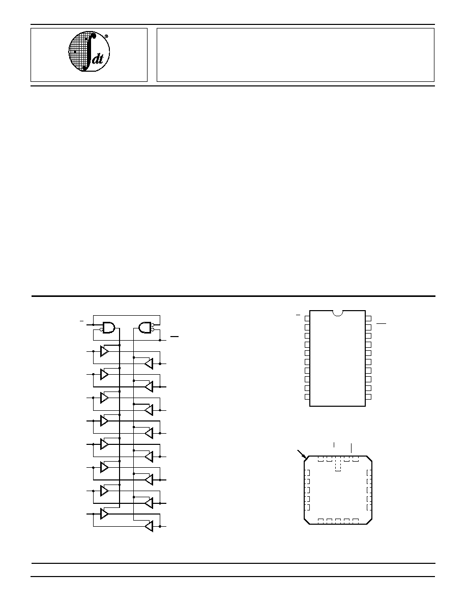
PIN CONFIGURATIONS
FUNCTIONAL BLOCK DIAGRAM
2539 drw 02
The IDT logo is a registered trademark of Integrated Device Technology, Inc.
LCC
TOP VIEW
5
6
7
8
9
10
A
1
A
2
A
3
1
2
3
4
20
19
18
17
16
15
14
13
Vcc
12
11
T/R
B
1
A
4
A
5
A
6
A
7
OE
B
2
B
3
B
4
B
5
B
6
GND
B
7
A
0
B
0
P20-1
D20-1
SO20-2
SO20-7*
SO20-8**
&
E20-1
INDEX
B
0
B
1
B
2
B
3
B
4
A
2
A
3
A
4
A
5
A
6
B
7
B
6
B
GND
A
7
A
0
A
1
Vcc
T/R
OE
15
14
5
18
17
16
5
6
7
8
4
L20-2
9 10 11 12 13
3
2
1
20 19
*FCT245T/2245T, FCT645T only.
**FCT245T/2245T, FCT640T
DIP/SOIC/SSOP/QSOP/CERPACK
TOP VIEW
FCT245T/2245T, FCT645T are non-inverting options.
FCT640T is the inverting options.
A
B
0
0
T/R
OE
A
B
1
1
A
B
2
2
A
B
3
3
A
B
4
4
A
B
5
5
A
B
6
6
A
B
7
7
2539 drw 03

6.9
2
IDT54/74FCT245T/AT/CT/DT - 2245T/AT/CT, IDT54/74FCT640T/AT/CT, IDT54/74FCT645T/AT/CT/DT
FAST CMOS OCTAL BIDIRECTIONAL TRANSCEIVERS
MILITARY AND COMMERCIAL TEMPERATURE RANGES
FUNCTION TABLE
(2)
2539 tbl 01
2539 tbl 02
NOTES:
1. 640 is inverting from input to output.
2. H = HIGH Voltage Level
L = LOW Voltage Level
X = Don't Care
ABSOLUTE MAXIMUM RATINGS
(1)
CAPACITANCE
(TA = +25
∞
C, F = 1.0MHZ)
Symbol
Rating
Commercial
Military
Unit
V
TERM(2)
Terminal Voltage
with Respect to
GND
≠0.5 to +7.0
≠0.5 to +7.0
V
V
TERM(3)
Terminal Voltage
with Respect to
GND
≠0.5 to
V
CC
+0.5
≠0.5 to
V
CC
+0.5
V
T
A
Operating
Temperature
0 to +70
≠55 to +125
∞
C
T
BIAS
Temperature
Under Bias
≠55 to +125
≠65 to +135
∞
C
T
STG
Storage
Temperature
≠55 to +125
≠65 to +150
∞
C
P
T
Power Dissipation
0.5
0.5
W
I
OUT
DC Output
Current
≠60 to +120 ≠60 to +120 mA
NOTES:
1. Stresses greater than those listed under ABSOLUTE MAXIMUM RAT-
INGS may cause permanent damage to the device. This is a stress rating
only and functional operation of the device at these or any other conditions
above those indicated in the operational sections of this specification is
not implied. Exposure to absolute maximum rating conditions for
extended periods may affect reliability. No terminal voltage may exceed
V
CC
by +0.5V unless otherwise noted.
2. Input and V
CC
terminals only.
3. Outputs and I/O terminals only.
2539 lnk 03
Symbol
Parameter
(1)
Conditions
Typ.
Max. Unit
C
IN
Input
Capacitance
V
IN
= 0V
6
10
pF
C
OUT
Output
Capacitance
V
OUT
= 0V
8
12
pF
2539 lnk 04
NOTE:
1. This parameter is measured at characterization but not tested.
PIN DESCRIPTION
Pin Names
Description
OE
Output Enable Input (Active LOW)
T/
R
Transmit/Receive Input
A
0
-A
7
Side A Inputs or 3-State Outputs
B
0
-B
7
Side B Inputs or 3-State Outputs
Inputs
OE
OE
T/
R
R
Outputs
L
L
Bus B Data to Bus A
(1)
L
H
Bus B Data to Bus B
(1)
H
X
High Z State

IDT54/74FCT245T/AT/CT/DT - 2245T/AT/CT, IDT54/74FCT640T/AT/CT, IDT54/74FCT645T/AT/CT/DT
FAST CMOS OCTAL BIDIRECTIONAL TRANSCEIVERS
MILITARY AND COMMERCIAL TEMPERATURE RANGES
6.9
3
DC ELECTRICAL CHARACTERISTICS OVER OPERATING RANGE
Following Conditions Apply Unless Otherwise Specified:
Commercial: T
A
= 0
∞
C to +70
∞
C, V
CC
= 5.0V
±
5%; Military: T
A
= ≠55
∞
C to +125
∞
C, V
CC
= 5.0V
±
10%
Symbol
Parameter
Test Conditions
(1)
Min.
Typ.
(2)
Max.
Unit
V
IH
Input HIGH Level
Guaranteed Logic HIGH Level
2.0
--
--
V
V
IL
Input LOW Level
Guaranteed Logic LOW Level
--
--
0.8
V
I
I H
Input HIGH Current
(4)
V
CC
= Max.
V
I
= 2.7V
--
--
±
1
µ
A
I
I L
Input LOW Current
(4)
V
I
= 0.5V
--
--
±
1
I
OZH
High Impedance Output Current
V
CC
= Max.
V
O
= 2.7V
--
--
±
1
µ
A
I
OZL
(3-State Output pins)
(4)
V
O
= 0.5V
--
--
±
1
I
I
Input HIGH Current
(4)
V
CC
= Max., V
I
= V
CC
(Max.)
--
--
±
1
µ
A
V
IK
Clamp Diode Voltage
V
CC
= Min., I
IN
= ≠18mA
--
≠0.7
≠1.2
V
V
H
Input Hysteresis
--
--
200
--
mV
I
CC
Quiescent Power Supply Current
V
CC
= Max., V
IN
= GND or V
CC
--
0.01
1
mA
OUTPUT DRIVE CHARACTERISTICS FOR FCT245T/640T/645T
Symbol
Parameter
Test Conditions
(1)
Min.
Typ.
(2)
Max.
Unit
V
OH
Output HIGH Voltage
V
CC
= Min.
V
IN
= V
IH
or V
IL
I
OH
= ≠6mA MIL.
I
OH
= ≠8mA COM'L.
2.4
3.3
--
V
I
OH
= ≠12mA MIL.
I
OH
= ≠15mA COM'L.
2.0
3.0
--
V
V
OL
Output LOW Voltage
V
CC
= Min.
V
IN
= V
IH
or V
IL
I
OL
= 48mA MIL.
I
OL
= 64mA COM'L.
--
0.3
0.55
V
I
OS
Short Circuit Current
V
CC
= Max., V
O
= GND
(3)
≠60
≠120
≠225
mA
OUTPUT DRIVE CHARACTERISTICS FOR FCT2245T
Symbol
Parameter
Test Conditions
(1)
Min.
Typ.
(2)
Max.
Unit
I
ODL
Output LOW Current
V
CC
= 5V, V
IN
= V
IH
or
V
IL,
V
OUT
= 1.5V
(3)
16
48
--
mA
I
ODH
Output HIGH Current
V
CC
= 5V, V
IN
= V
IH
or V
IL,
V
OUT
= 1.5V
(3)
≠16
≠48
--
mA
V
OH
Output HIGH Voltage
V
CC
= Min.
V
IN
= V
IH
or
V
IL
I
OH
= ≠12mA MIL.
I
OH
= ≠15mA COM'L.
2.4
3.3
--
V
V
OL
Output LOW Voltage
V
CC
= Min.
V
IN
= V
IH
or V
IL
I
OL
= 12mA
--
0.3
0.50
V
2539 lnk 05
2539 lnk 06
2539 lnk 07
NOTES:
1. For conditions shown as Max. or Min., use appropriate value specified under Electrical Characteristics for the applicable device type.
2. Typical values are at Vcc = 5.0V, +25
∞
C ambient.
3. Not more than one output should be shorted at one time. Duration of the short circuit test should not exceed one second.
4. The test limit for this parameter is
±
5
µ
A at T
A
= ≠55
∞
C.

6.9
4
IDT54/74FCT245T/AT/CT/DT - 2245T/AT/CT, IDT54/74FCT640T/AT/CT, IDT54/74FCT645T/AT/CT/DT
FAST CMOS OCTAL BIDIRECTIONAL TRANSCEIVERS
MILITARY AND COMMERCIAL TEMPERATURE RANGES
POWER SUPPLY CHARACTERISTICS
NOTES:
1. For conditions shown as Max. or Min., use appropriate value specified under Electrical Characteristics for the applicable device type.
2. Typical values are at V
CC
= 5.0V, +25
∞
C ambient.
3. Per TTL driven input (V
IN
= 3.4V). All other inputs at V
CC
or GND.
4. This parameter is not directly testable, but is derived for use in Total Power Supply Calculations.
5. Values for these conditions are examples of the I
CC
formula. These limits are guaranteed but not tested.
6. I
C
= I
QUIESCENT
+ I
INPUTS
+ I
DYNAMIC
I
C
= I
CC
+
I
CC
D
H
N
T
+ I
CCD
(f
CP/
2 + f
i
N
i
)
I
CC
= Quiescent Current
I
CC
= Power Supply Current for a TTL High Input (V
IN
= 3.4V)
D
H
= Duty Cycle for TTL Inputs High
N
T
= Number of TTL Inputs at D
H
I
CCD
= Dynamic Current Caused by an Input Transition Pair (HLH or LHL)
f
CP
= Clock Frequency for Register Devices (Zero for Non-Register Devices)
f
i
= Input Frequency
N
i
= Number of Inputs at f
i
All currents are in milliamps and all frequencies are in megahertz.
2539 tbl 08
Symbol
Parameter
Test Conditions
(1)
Min.
Typ.
(2)
Max.
Unit
I
CC
Quiescent Power Supply Current
TTL Inputs HIGH
V
CC
= Max.
V
IN
= 3.4V
(3)
--
0.5
2.0
mA
I
CCD
Dynamic Power Supply
Current
(4)
V
CC
= Max.
Outputs Open
V
IN
= V
CC
V
IN
= GND
FCTxxxT
--
0.15
0.25
mA/
MHz
OE
= T/
R
= GND
One Input Toggling
50% Duty Cycle
FCT2xxxT
--
0.06
0.12
I
C
Total Power Supply Current
(6)
V
CC
= Max.
V
IN
= V
CC
FCTxxxT
--
1.5
3.5
mA
Outputs Open
fi = 10MHz
V
IN
= GND FCT2xxxT
--
0.6
2.2
50% Duty Cycle
V
IN
= 3.4
FCTxxxT
--
1.8
4.5
OE
= T/
R
= GND
One Bit Toggling
V
IN
= GND FCT2xxxT
0.9
3.2
V
CC
= Max.
V
IN
= V
CC
FCTxxxT
--
3.0
6.0
(5)
Outputs Open
fi = 2.5MHz
V
IN
= GND FCT2xxxT
--
1.2
3.4
(5)
50% Duty Cycle
V
IN
= 3.4
FCTxxxT
--
5.0
14.0
(5)
OE
= T/
R
= GND
Eight Bits Toggling
V
IN
= GND FCT2xxxT
--
3.2
11.4
(
5)
IDT54/74FCT245T/AT/CT/DT - 2245T/AT/CT, IDT54/74FCT640T/AT/CT, IDT54/74FCT645T/AT/CT/DT
FAST CMOS OCTAL BIDIRECTIONAL TRANSCEIVERS
MILITARY AND COMMERCIAL TEMPERATURE RANGES
6.9
5
SWITCHING CHARACTERISTICS OVER OPERATING RANGE
2534 tbl 09
SWITCHING CHARACTERISTICS OVER OPERATING RANGE
2534 tbl 10
FCT245T
FCT2245T
FCT245AT
FCT2245AT
Com'l.
Mil.
Com'l.
Mil.
Symbol
Parameter
Conditions
(1)
Min.
(2)
Max.
Min
.
(2)
Max.
Min
.
(2)
Max.
Min.
(2)
Max.
Unit
t
PLH
t
PHL
Propagation Delay
A to B, B to A
C
L
= 50 pF
R
L
= 500
1.5
7.0
1.5
7.5
1.5
4.6
1.5
4.9
ns
t
PZH
t
PZL
Output Enable Time
OE
to A or B
1.5
9.5
1.5
10.0
1.5
6.2
1.5
6.5
ns
t
PHZ
t
PLZ
Output Disable Time
OE
to A or B
1.5
7.5
1.5
10.0
1.5
5.0
1.5
6.0
ns
t
PZH
t
PZL
Output Enable Time
T/
R
to A or B
(3)
1.5
9.5
1.5
10.0
1.5
6.2
1.5
6.5
ns
t
PHZ
t
PLZ
Output Disable Time
T/
R
to A or B
(3)
1.5
7.5
1.5
10.0
1.5
5.0
1.5
6.0
ns
FCT245CT
FCT2245CT
FCT245DT
Com'l.
Mil.
Com'l.
Mil.
Symbol
Parameter
Conditions
(1)
Min.
(2)
Max.
Min
.
(2)
Max.
Min
.
(2)
Max.
Min.
(2)
Max.
Unit
t
PLH
t
PHL
Propagation Delay
A to B, B to A
C
L
= 50 pF
R
L
= 500
1.5
4.1
1.5
4.5
1.5
3.8
--
--
ns
t
PZH
t
PZL
Output Enable Time
OE
to A or B
1.5
5.8
1.5
6.2
1.5
5.0
--
--
ns
t
PHZ
t
PLZ
Output Disable Time
OE
to A or B
1.5
4.8
1.5
5.2
1.5
4.3
--
--
ns
t
PZH
t
PZL
Output Enable Time
T/
R
to A or B
(3)
1.5
5.8
1.5
6.2
1.5
5.0
--
--
ns
t
PHZ
t
PLZ
Output Disable Time
T/
R
to A or B
(3)
1.5
4.8
1.5
5.2
1.5
4.3
--
--
ns
FCT640T
FCT640AT
FCT640CT
Com'l.
Mil.
Com'l.
Mil.
Com'l.
Mil.
Symbol
Parameter
Conditions
(1)
Min
.
(2)
Max. Min.
(2)
Max. Min
.
(2)
Max. Min.
(2)
Max. Min.
(2)
Max. Min.
(2)
Max.
Unit
t
PLH
t
PHL
Propagation Delay
A to B, B to A
C
L
= 50 pF
R
L
= 500
2.0
7.0
2.0
8.0
1.5
5.0
1.5
5.3
1.5
4.4
1.5
4.7
ns
t
PZH
t
PZL
Output Enable Time
OE
to A or B
2.0
13.0
2.0
16.0
1.5
6.2
1.5
6.5
1.5
5.8
1.5
6.2
ns
t
PHZ
t
PLZ
Output Disable Time
OE
to A or B
2.0
10.0
2.0
12.0
1.5
5.0
1.5
6.0
1.5
4.8
1.5
5.2
ns
t
PZH
t
PZL
Output Enable Time
T/
R
to A or B
(3)
2.0
13.0
2.0
16.0
1.5
6.2
1.5
6.5
1.5
5.8
1.5
6.2
ns
t
PHZ
t
PLZ
Output Disable Time
T/
R
to A or B
(3)
2.0
10.0
2.0
12.0
1.5
5.0
1.5
6.0
1.5
4.8
1.5
5.2
ns
NOTES:
2534 tbl 11
1. See test circuit and waveforms.
2. Minimum limits are guaranteed but not tested on Propagation Delays.
3. This parameter is guaranteed but not tested.

6.9
6
IDT54/74FCT245T/AT/CT/DT - 2245T/AT/CT, IDT54/74FCT640T/AT/CT, IDT54/74FCT645T/AT/CT/DT
FAST CMOS OCTAL BIDIRECTIONAL TRANSCEIVERS
MILITARY AND COMMERCIAL TEMPERATURE RANGES
SWITCHING CHARACTERISTICS OVER OPERATING RANGE
FCT645T
FCT645AT
Com'l.
Mil.
Com'l.
Mil.
Symbol
Parameter
Conditions
(1)
Min.
(2)
Max.
Min
.
(2)
Max.
Min
.
(2)
Max.
Min.
(2)
Max.
Unit
t
PLH
t
PHL
Propagation Delay
A to B, B to A
C
L
= 50 pF
R
L
= 500
1.5
9.5
1.5
11.0
1.5
4.6
1.5
4.9
ns
t
PZH
t
PZL
Output Enable Time
OE
to A or B
1.5
11.0
1.5
12.0
1.5
6.2
1.5
6.5
ns
t
PHZ
t
PLZ
Output Disable Time
OE
to A or B
1.5
12.0
1.5
13.0
1.5
5.0
1.5
6.0
ns
t
PZH
t
PZL
Output Enable Time
T/
R
to A or B
(3)
1.5
11.0
1.5
12.0
1.5
6.2
1.5
6.5
ns
t
PHZ
t
PLZ
Output Disable Time
T/
R
to A or B
(3)
1.5
12.0
1.5
13.0
1.5
5.0
1.5
6.0
ns
2534 tbl 12
FCT645CT
FCT645DT
Com'l.
Mil.
Com'l.
Mil.
Symbol
Parameter
Conditions
(1)
Min.
(2)
Max.
Min
.
(2)
Max.
Min
.
(2)
Max.
Min.
(2)
Max.
Unit
t
PLH
t
PHL
Propagation Delay
A to B, B to A
C
L
= 50 pF
R
L
= 500
1.5
4.1
1.5
4.5
1.5
3.8
--
--
ns
t
PZH
t
PZL
Output Enable Time
OE
to A or B
1.5
5.8
1.5
6.2
1.5
5.0
--
--
ns
t
PHZ
t
PLZ
Output Disable Time
OE
to A or B
1.5
4.8
1.5
5.2
1.5
4.3
--
--
ns
t
PZH
t
PZL
Output Enable Time
T/
R
to A or B
(3)
1.5
5.8
1.5
6.2
1.5
5.0
--
--
ns
t
PHZ
t
PLZ
Output Disable Time
T/
R
to A or B
(3)
1.5
4.8
1.5
5.2
1.5
4.3
--
--
ns
NOTES:
2534 tbl 13
1. See test circuit and waveforms.
2. Minimum limits are guaranteed but not tested on Propagation Delays.
3. This parameter is guaranteed but not tested.
IDT54/74FCT245T/AT/CT/DT - 2245T/AT/CT, IDT54/74FCT640T/AT/CT, IDT54/74FCT645T/AT/CT/DT
FAST CMOS OCTAL BIDIRECTIONAL TRANSCEIVERS
MILITARY AND COMMERCIAL TEMPERATURE RANGES
6.9
7
TEST CIRCUITS AND WAVEFORMS
TEST CIRCUITS FOR ALL OUTPUTS
SET-UP, HOLD AND RELEASE TIMES
PULSE WIDTH
SWITCH POSITION
Pulse
Generator
R
T
D.U.T.
V
CC
V
IN
C
L
V
OUT
50pF
500
500
7.0V
3V
1.5V
0V
3V
1.5V
0V
3V
1.5V
0V
3V
1.5V
0V
DATA
INPUT
TIMING
INPUT
ASYNCHRONOUS CONTROL
PRESET
CLEAR
ETC.
SYNCHRONOUS CONTROL
t
SU
t
H
t
REM
t
SU
t
H
HIGH-LOW-HIGH
PULSE
LOW-HIGH-LOW
PULSE
t
W
1.5V
1.5V
SAME PHASE
INPUT TRANSITION
3V
1.5V
0V
1.5V
V
OH
t
PLH
OUTPUT
OPPOSITE PHASE
INPUT TRANSITION
3V
1.5V
0V
t
PLH
t
PHL
t
PHL
V
OL
CONTROL
INPUT
3V
1.5V
0V
3.5V
0V
OUTPUT
NORMALLY
LOW
OUTPUT
NORMALLY
HIGH
SWITCH
CLOSED
SWITCH
OPEN
V
OL
0.3V
0.3V
t
PLZ
t
PZL
t
PZH
t
PHZ
3.5V
0V
1.5V
1.5V
ENABLE
DISABLE
V
OH
PRESET
CLEAR
CLOCK ENABLE
ETC.
ENABLE AND DISABLE TIMES
PROPAGATION DELAY
NOTES:
1. Diagram shown for input Control Enable-LOW and input Control Disable-
HIGH
2. Pulse Generator for All Pulses: Rate
1.0MHz; t
F
2.5ns; t
R
2.5ns
Test
Switch
Disable Low
Enable Low
Closed
All Other Tests
Open
Open Drain
DEFINITIONS:
C
L
=
Load capacitance: includes jig and probe capacitance.
R
T
=
Termination resistance: should be equal to Z
OUT
of the Pulse
Generator.
2534 drw 04
2534 drw 05
2534 drw 06
2534 drw 07
2534 drw 08
2534 lnk 14

6.9
8
IDT54/74FCT245T/AT/CT/DT - 2245T/AT/CT, IDT54/74FCT640T/AT/CT, IDT54/74FCT645T/AT/CT/DT
FAST CMOS OCTAL BIDIRECTIONAL TRANSCEIVERS
MILITARY AND COMMERCIAL TEMPERATURE RANGES
ORDERING INFORMATION
XX
X
Package
X
Process
Blank
B
Commercial
MIL-STD-883, Class B
P
D
SO
L
E
PY
Q
Plastic DIP
CERDIP
Small Outline IC
Leadless Chip Carrier
CERPACK
Shrink Small Outline Package
Quarter-size Small Outline Package
245T
640T
645T
245AT
640AT
645AT
245CT
640CT
645CT
245DT
645DT
Non-Inverting Octal Bidirectional Transceiver
Inverting Octal Bidirectional Transceiver
Non-Inverting Octal Bidirectional Transceiver
X
Device
Type
High Drive
Balanced Drive
Blank
2
Temperature
Range
FCT
IDT
≠55
∞
C to +125
∞
C
0
∞
C to +70
∞
C
54
74
Family
X
2539 drw 09