Äîêóìåíòàöèÿ è îïèñàíèÿ www.docs.chipfind.ru
Integrated Device Technology, Inc.
MILITARY AND COMMERCIAL TEMPERATURE RANGES
MAY 1992
©
1992 Integrated Device Technology, Inc.
7.12
DSC-4624/2
®
FEATURES
· IDT54/74FCT373/533/573 equivalent to FAST
TM
speed
and drive
· IDT54/74FCT373A/533A/573A up to 30% faster than
FAST
· Equivalent to FAST output drive over full temperature
and voltage supply extremes
· I
OL
= 48mA (commercial) and 32mA (military)
· CMOS power levels (1mW typ. static)
· Octal transparent latch with 3-state output control
· JEDEC standard pinout for DIP and LCC
· Product available in Radiation Tolerant and Radiation
Enhanced versions
· Military product compliant to MIL-STD-883, Class B
DESCRIPTION
The IDT54/74FCT373/A/C, IDT54/74FCT533/A/C and
IDT54/74FCT573/A/C are octal transparent latches built us-
ing an advanced dual metal CMOS technology. These octal
latches have 3-state outputs and are intended for bus oriented
applications. The flip-flops appear transparent to the data
when Latch Enable (LE) is HIGH. When LE is LOW, the data
that meets the set-up time is latched. Data appears on the bus
when the Output Enable (
OE
) is LOW. When
OE
is HIGH, the
bus output is in the high-impedance state.
2602 cnv* 02
FAST CMOS OCTAL
TRANSPARENT LATCHES
IDT54/74FCT373/A/C
IDT54/74FCT533/A/C
IDT54/74FCT573/A/C
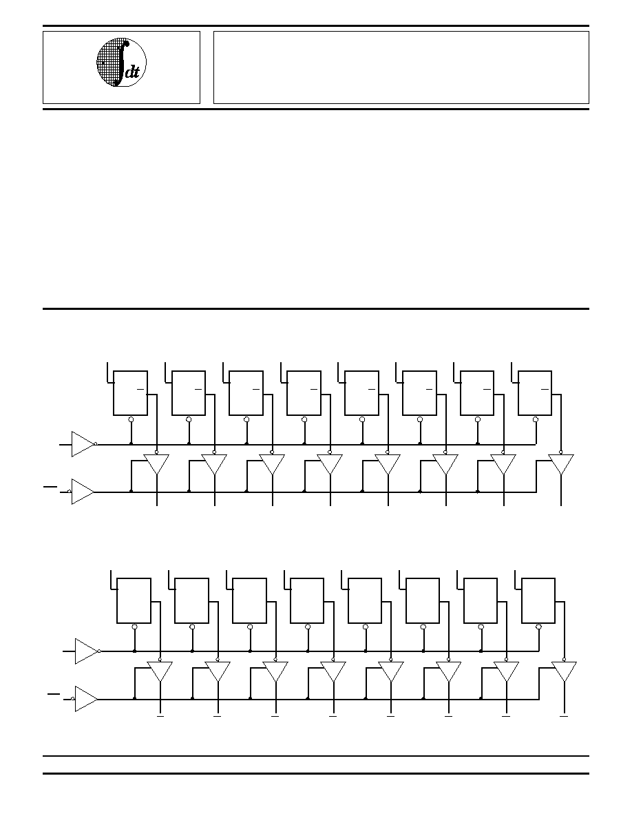
FUNCTIONAL BLOCK DIAGRAMS
IDT54/74FCT373 AND IDT54/74FCT573
IDT54/74FCT533
The IDT logo is a registered trademark of Integrated Device Technology, Inc.
FAST is a trademark of National Semiconductor Co.
2602 cnv* 01
D
0
D
O
G
O
0
D
1
D
O
G
O
1
D
2
D
O
G
O
2
D
3
D
O
G
O
3
D
4
D
O
G
O
4
D
5
D
O
G
O
5
D
6
D
O
G
O
6
D
7
D
O
G
O
7
LE
OE
D
0
D
O
G
O
0
D
1
D
O
G
O
1
D
2
D
O
G
O
2
D
3
D
O
G
O
3
D
4
D
O
G
O
4
D
5
D
O
G
O
5
D
6
D
O
G
O
6
D
7
D
O
G
O
7
LE
OE
1
7.12
2
IDT54/74FCT373/533/573/A/C
FAST CMOS OCTAL TRANSPARENT LATCHES
MILITARY AND COMMERCIAL TEMPERATURE RANGES
PIN CONFIGURATIONS
IDT54/74FCT373
2602 cnv* 0308
IDT54/74FCT573
IDT54/74FCT533
OE
O
0
D
0
D
1
O
1
O
2
D
2
D
3
O
3
GND
O
7
D
7
D
6
O
6
O
5
D
4
LE
D
5
O
4
V
CC
1
2
3
4
5
6
7
8
9
10
11
12
13
14
15
16
17
18
19
20
DIP/SOIC/CERPACK
TOP VIEW
P20-1
D20-1
SO20-2
&
E20-1
INDEX
D
1
O
1
O
2
D
2
D
3
D
7
D
6
O
6
O
5
D
5
O
0
D
0
OE
V
CC
O
7
O
3
GND
LE
O
4
D
4
LCC
TOP VIEW
3
2
20 19
1
4
5
6
7
8
18
17
16
15
14
9 10 11 12 13
L20-2
D
0
D
1
D
2
D
3
D
4
D
5
D
6
D
7
GND
O
0
O
1
O
2
O
3
O
4
O
6
LE
O
5
O
7
V
CC
1
2
3
4
5
6
7
8
9
10
11
12
13
14
15
16
17
18
19
20
DIP/SOIC/CERPACK
TOP VIEW
P20-1
D20-1
SO20-2
&
E20-1
INDEX
D
2
D
3
D
4
D
5
D
6
O
1
O
2
O
3
O
4
O
5
D
0
D
1
V
CC
O
0
D
7
GND
LE
O
7
O
6
LCC
TOP VIEW
3
2
20 19
1
4
5
6
7
8
18
17
16
15
14
9 10 11 12 13
L20-2
OE
OE
OE
O
0
D
0
D
1
O
1
O
2
D
2
D
3
O
3
GND
O
7
D
7
D
6
O
6
O
5
D
4
LE
D
5
O
4
V
CC
1
2
3
4
5
6
7
8
9
10
11
12
13
14
15
16
17
18
19
20
DIP/SOIC/CERPACK
TOP VIEW
P20-1
D20-1
SO20-2
&
E20-1
INDEX
D
1
D
7
O
0
D
0
OE
V
CC
O
7
GND
LCC
TOP VIEW
D
6
O
6
O
5
D
5
O
1
O
2
D
2
D
3
LE
O
4
D
4
O
3
3
2
20 19
1
4
5
6
7
8
18
17
16
15
14
9 10 11 12 13
L20-2
7.12
3
IDT54/74FCT373/533/573/A/C
FAST CMOS OCTAL TRANSPARENT LATCHES
MILITARY AND COMMERCIAL TEMPERATURE RANGES
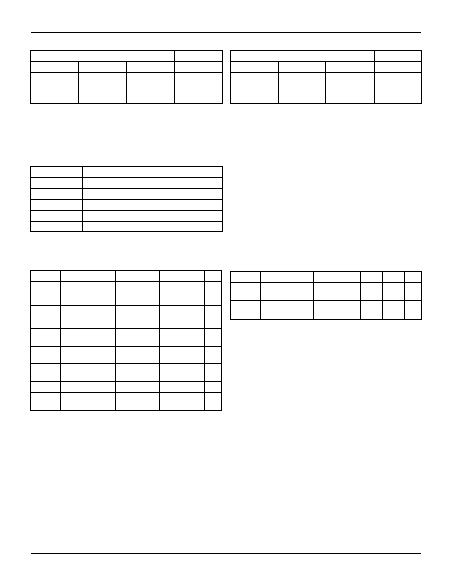
FUNCTION TABLE (FCT533)
(1)
FUNCTION TABLE (FCT373 and FCT573)
(1)
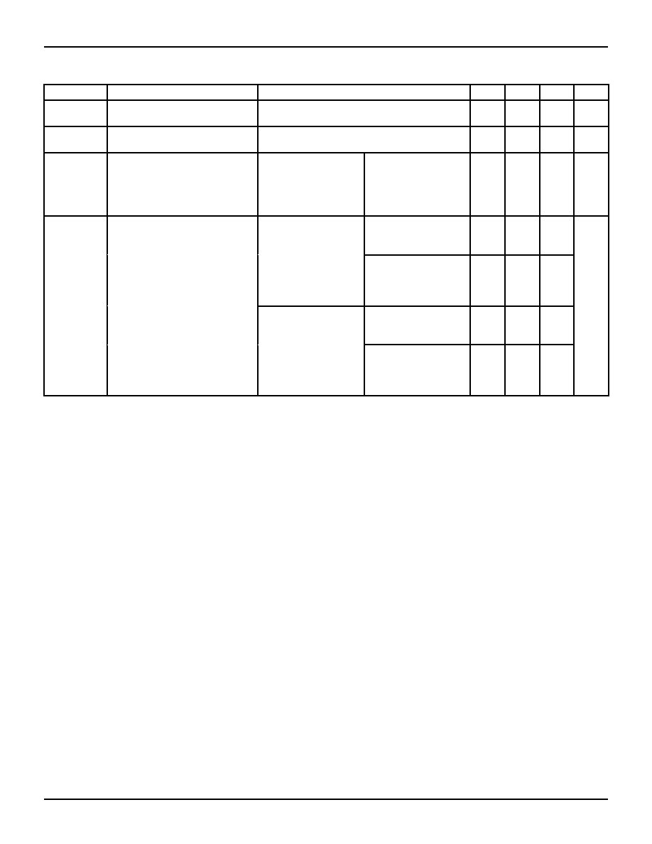
PIN DESCRIPTION
2602 tbl 07
ABSOLUTE MAXIMUM RATINGS
(1)
CAPACITANCE
(T
A
= +25
°
C, f = 1.0MHz)
Symbol
Parameter
Conditions
Typ.
Max.
Unit
C
IN
Input
Capacitance
V
IN
= 0V
6
10
pF
C
OUT
Output
Capacitance
V
OUT
= 0V
8
12
pF
NOTE:
2602 tbl 02
1. This parameter is measured at characterization but not tested.
NOTE:
2602 tbl 05
1. H = HIGH Voltage Level
L = LOW Voltage Level
X = Don't Care
Z = High Impedance
NOTE:
2602 tbl 06
1. H = HIGH Voltage Level
L = LOW Voltage Level
X = Don't Care
Z = High Impedance
NOTES:
2602 tbl 01
1. Stresses greater than those listed under ABSOLUTE MAXIMUM
RATINGS may cause permanent damage to the device. This is a stress
rating only and functional operation of the device at these or any other
conditions above those indicated in the operational sections of this
specification is not implied. Exposure to absolute maximum rating
conditions for extended periods may affect reliability. No terminal voltage
may exceed V
CC
by +0.5V unless otherwise noted.
2. Input and V
CC
terminals only.
3. Outputs and I/O terminals only.
Symbol
Rating
Commercial
Military
Unit
V
TERM(2)
Terminal Voltage
with Respect to
GND
0.5 to +7.0
0.5 to +7.0
V
V
TERM(3)
Terminal Voltage
with Respect to
GND
0.5 to V
CC
0.5 to V
CC
V
T
A
Operating
Temperature
0 to +70
55 to +125
°
C
T
BIAS
Temperature
Under Bias
55 to +125
65 to +135
°
C
T
STG
Storage
Temperature
55 to +125
65 to +150
°
C
P
T
Power Dissipation
0.5
0.5
W
I
OUT
DC Output
Current
120
120
mA
Inputs
Outputs
D
N
LE
OE
OE
O
N
H
H
L
H
L
H
L
L
X
X
H
Z
Inputs
Outputs
D
N
LE
OE
OE
O
O
N
H
H
L
L
L
H
L
H
X
X
H
Z
Pin Names
Description
D
N
Data Inputs
LE
Latch Enable Input (Active HIGH)
OE
Output Enable Input (Active LOW)
O
N
3-State Outputs
O
N
Complementary 3-State Outputs
7.12
4
IDT54/74FCT373/533/573/A/C
FAST CMOS OCTAL TRANSPARENT LATCHES
MILITARY AND COMMERCIAL TEMPERATURE RANGES
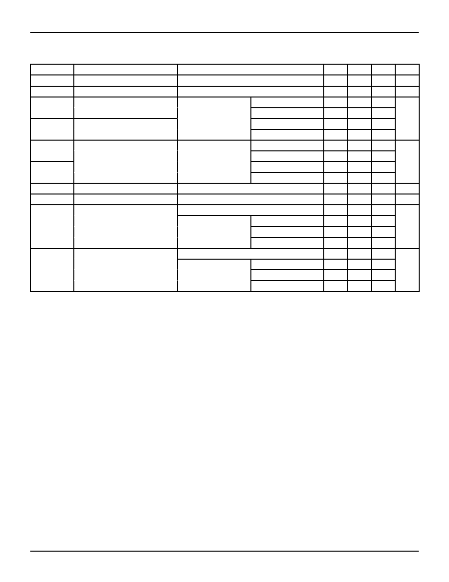
DC ELECTRICAL CHARACTERISTICS OVER OPERATING RANGE
Following Conditions Apply Unless Otherwise Specified: V
LC
= 0.2V; V
HC
= V
CC
0.2V
Commercial: T
A
= 0
°
C to +70
°
C, V
CC
= 5.0V
±
5%; Military: T
A
= 55
°
C to +125
°
C, V
CC
= 5.0V
±
10%
NOTES:
2602 tbl 03
1. For conditions shown as Max. or Min., use appropriate value specified under Electrical Characteristics for the applicable device type.
2. Typical values are at V
CC
= 5.0V, +25
°
C ambient and maximum loading.
3. Not more than one output should be shorted at one time. Duration of the short circuit test should not exceed one second.
4. This parameter is guaranteed but not tested.
Symbol
Parameter
Test Conditions
(1)
Min.
Typ.
(2)
Max.
Unit
V
IH
Input HIGH Level
Guaranteed Logic HIGH Level
2.0
--
--
V
V
IL
Input LOW Level
Guaranteed Logic LOW Level
--
--
0.8
V
I
I H
Input HIGH Current
V
CC
= Max.
V
I
= V
CC
--
--
5
µ
A
V
I
= 2.7V
--
--
5
(4)
I
I L
Input LOW Current
V
I
= 0.5V
--
--
5
(4)
V
I
= GND
--
--
5
I
OZH
Off State (High Impedance)
V
CC
= Max.
V
O
= V
CC
--
--
10
µ
A
Output Current
V
O
= 2.7V
--
--
10
(4)
I
OZL
V
O
= 0.5V
--
--
10
(4)
V
O
= GND
--
--
10
V
IK
Clamp Diode Voltage
V
CC
= Min., I
N
= 18mA
--
0.7
1.2
V
I
OS
Short Circuit Current
V
CC
= Max.
(3)
, V
O
= GND
60
120
--
mA
V
OH
Output HIGH Voltage
V
CC
= 3V, V
IN
= V
LC
or V
HC
, I
OH
= 32
µ
A
V
HC
V
CC
--
V
V
CC
= Min.
I
OH
= 300
µ
A
V
HC
V
CC
--
V
IN
= V
IH
or V
IL
I
OH
= 12mA MIL.
2.4
4.3
--
I
OH
= 15mA COM'L.
2.4
4.3
--
V
OL
Output LOW Voltage
V
CC
= 3V, V
IN
= V
LC
or V
HC
, I
OL
= 300
µ
A
--
GND
V
LC
V
V
CC
= Min.
I
OL
= 300
µ
A
--
GND
V
LC(4)
V
IN
= V
IH
or V
IL
I
OL
= 32mA MIL.
--
0.3
0.5
I
OL
= 48mA COM'L.
--
0.3
0.5
7.12
5
IDT54/74FCT373/533/573/A/C
FAST CMOS OCTAL TRANSPARENT LATCHES
MILITARY AND COMMERCIAL TEMPERATURE RANGES
POWER SUPPLY CHARACTERISTICS
V
LC
= 0.2V; V
HC
= V
CC
0.2V
NOTES:
2602 tbl 04
1. For conditions shown as Max. or Min., use appropriate value specified under Electrical Characteristics for the applicable device type.
2. Typical values are at V
CC
= 5.0V, +25
°
C ambient.
3. Per TTL driven input (V
IN
= 3.4V); all other inputs at V
CC
or GND.
4. This parameter is not directly testable, but is derived for use in Total Power Supply Calculations.
5. Values for these conditions are examples of the I
CC
formula. These limits are guaranteed but not tested.
6. I
C
= I
QUIESCENT
+ I
INPUTS
+ I
DYNAMIC
I
C
= I
CC
+
I
CC
D
H
N
T
+ I
CCD
(f
CP
/2 + f
i
N
i
)
I
CC
= Quiescent Current
I
CC
= Power Supply Current for a TTL High Input (V
IN
= 3.4V)
D
H
= Duty Cycle for TTL Inputs High
N
T
= Number of TTL Inputs at D
H
I
CCD
= Dynamic Current Caused by an Input Transition Pair (HLH or LHL)
f
CP
= Clock Frequency for Register Devices (Zero for Non-Register Devices)
f
i
= Input Frequency
N
i
= Number of Inputs at f
i
All currents are in milliamps and all frequencies are in megahertz.
Symbol
Parameter
Test Conditions
(1)
Min.
Typ.
(2)
Max.
Unit
I
CC
Quiescent Power Supply Current
V
CC
= Max.
V
IN
V
HC
; V
IN
V
LC
--
0.2
1.5
mA
I
CC
Quiescent Power Supply Current
TTL Inputs HIGH
V
CC
= Max.
V
IN
= 3.4V
(3)
--
0.5
2.0
mA
I
CCD
Dynamic Power Supply
Current
(4)
V
CC
= Max.
Outputs Open
OE
= GND
One Input Toggling
50% Duty Cycle
V
IN
V
HC
V
IN
V
LC
--
0.15
0.25
mA/
MHz
I
C
Total Power Supply Current
(6)
V
CC
= Max.
Outputs Open
fi = 10MHz
V
IN
V
HC
V
IN
V
LC
(FCT)
--
1.7
4.0
mA
50% Duty Cycle
OE
= GND
LE
=
V
CC
One Bit Toggling
V
IN
= 3.4V
V
IN
= GND
--
2.0
5.0
V
CC
= Max.
Outputs Open
fi = 2.5MHz
V
IN
V
HC
V
IN
V
LC
(FCT)
--
3.2
6.5
(5)
50% Duty Cycle
OE
= GND
LE
=
V
CC
Eight Bits Toggling
V
IN
= 3.4V
V
IN
= GND
--
5.2
14.5
(5)