Integrated Device Technology, Inc.
Æ
FEATURES:
∑ IDT54/74FCT374/534/574 equivalent to FAST
TM
speed
and drive
∑ IDT54/74FCT374A/534A/574A up to 30% faster than
FAST
∑ IDT54/74FCT374C/534C/574C up to 50% faster than
FAST
∑ I
OL
= 48mA (commercial) and 32mA (military)
∑ CMOS power levels (1mW typ. static)
∑ Edge triggered master/slave, D-type flip-flops
∑ Buffered common clock and buffered common three-
state control
∑ Product available in Radiation Tolerant and Radiation
Enhanced versions
∑ Military product compliant to MIL-STD-883, Class B
∑ Meets or exceeds JEDEC Standard 18 specifications
DESCRIPTION:
The IDT54/74FCT374/A/C, IDT54/74FCT534/A/C and
IDT54/74FCT574/A/C are 8-bit registers built using an ad-
vanced dual metal CMOS technology. These registers consist
of eight D-type flip-flops with a buffered common clock and
buffered 3-state output control. When the output enable (
OE
)
is LOW, the eight outputs are enabled. When the
OE
input is
HIGH, the outputs are in the high-impedance state.
Input data meeting the set-up and hold time requirements
of the D inputs is transferred to the O outputs on the LOW-to-
HIGH transition of the clock input.
The IDT54/74FCT374/A/C and IDT54/74FCT574/A/ C have
non-inverting outputs with respect to the data at the D inputs.
The IDT54/74FCT534/A/C have inverting outputs.
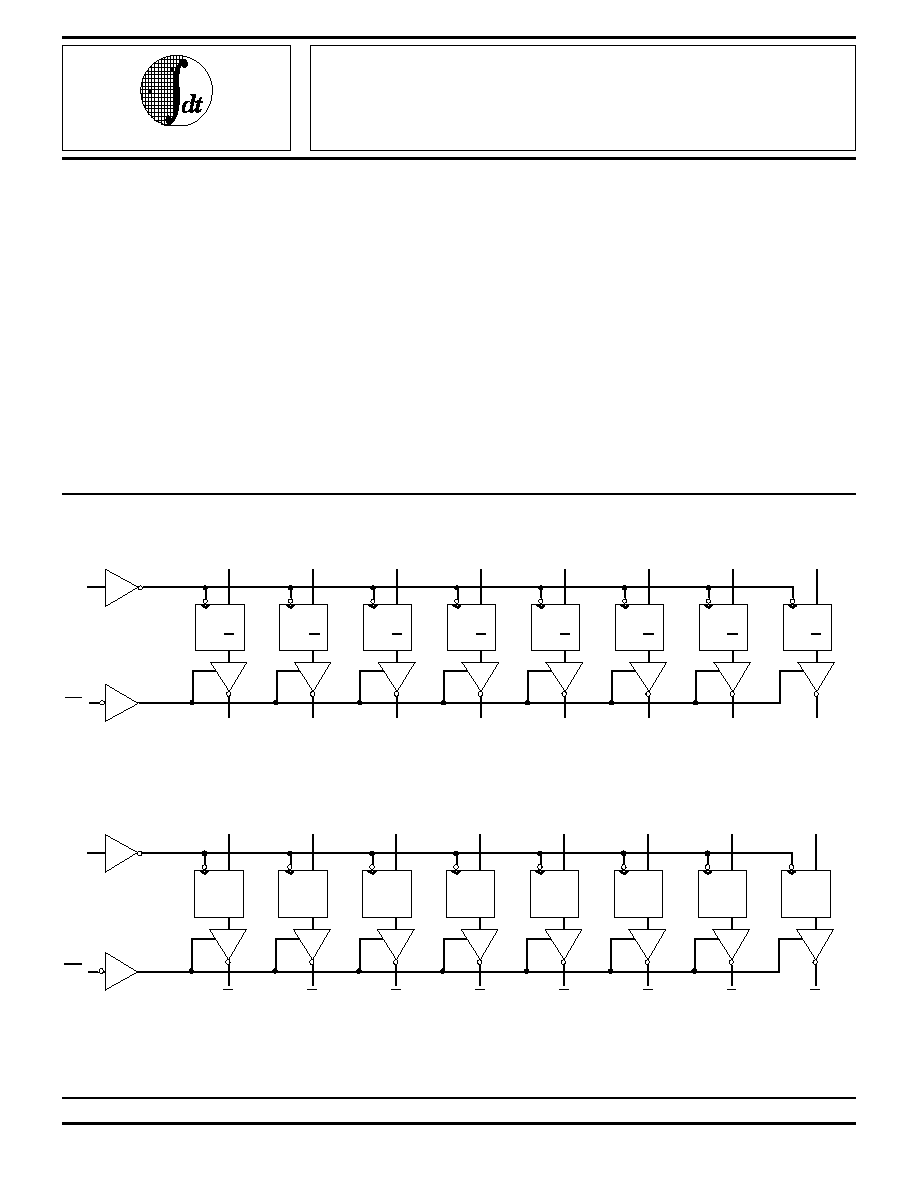
FUNCTIONAL BLOCK DIAGRAM IDT54/74FCT374 AND IDT54/74FCT574
D
0
O
0
D
1
O
1
D
2
O
2
D
3
O
3
D
4
O
4
D
5
O
5
D
6
O
6
D
7
O
7
CP
OE
D
Q
CP
D
Q
CP
D
Q
CP
D
Q
CP
D
Q
CP
D
Q
CP
D
Q
CP
D
Q
CP
FUNCTIONAL BLOCK DIAGRAM IDT54/74FCT534
D
0
O
0
D
1
O
1
D
2
O
2
D
3
O
3
D
4
O
4
D
5
O
5
D
6
O
6
D
7
O
7
CP
OE
D
Q
CP
D
Q
CP
D
Q
CP
D
Q
CP
D
Q
CP
D
Q
CP
D
Q
CP
D
Q
CP
The IDT logo is a registered trademark of Integrated Device Technology, Inc.
FAST is a trademark of National Semiconductor, Inc.
2603 cnv* 01
2603 cnv* 02
IDT54/74FCT374/A/C
IDT54/74FCT534/A/C
IDT54/74FCT574/A/C
FAST CMOS OCTAL D
REGISTERS (3-STATE)
MILITARY AND COMMERCIAL TEMPERATURE RANGES
MAY 1992
©
1992 Integrated Device Technology, Inc.
7.13
DSC-4622/2
1
7.13
2
IDT54/74FCT374/534/574/A/C
FAST CMOS OCTAL D REGISTERS (3-STATE)
MILITARY AND COMMERCIAL TEMPERATURE RANGES
OE
O
0
D
0
D
1
O
1
O
2
D
2
D
3
O
3
GND
O
7
D
7
D
6
O
6
O
5
D
4
CP
D
5
O
4
V
CC
1
2
3
4
5
6
7
8
9
10
11
12
13
14
15
16
17
18
19
20
DIP/SOIC/CERPACK
TOP VIEW
P20-1
D20-1
SO20-2
&
E20-1
IDT54/74FCT534
2603 cnv* 03
2603 cnv* 04
INDEX
D
1
O
1
O
2
D
2
D
3
D
7
D
6
O
6
O
5
D
5
O
0
D
0
OE
V
CC
O
7
O
3
GND
CP
O
4
D
4
LCC
TOP VIEW
3
2
20 19
1
4
5
6
7
8
18
17
16
15
14
9 10 11 12 13
L20-2
2603 cnv* 05
2603 cnv* 06
2603 cnv* 07
2603 cnv* 08
PIN CONFIGURATIONS
IDT54/74FCT374
IDT54/74FCT574
OE
D
0
D
1
D
2
D
3
D
4
D
5
D
6
D
7
GND
O
0
O
1
O
2
O
3
O
4
O
6
CP
O
5
O
7
V
CC
1
2
3
4
5
6
7
8
9
10
11
12
13
14
15
16
17
18
19
20
DIP/SOIC/CERPACK
TOP VIEW
P20-1
D20-1
SO20-2
&
E20-1
OE
O
0
D
0
D
1
O
1
O
2
D
2
D
3
O
3
GND
O
7
D
7
D
6
O
6
O
5
D
4
CP
D
5
O
4
V
CC
1
2
3
4
5
6
7
8
9
10
11
12
13
14
15
16
17
18
19
20
DIP/SOIC/CERPACK
TOP VIEW
P20-1
D20-1
SO20-2
&
E20-1
INDEX
D
2
D
3
D
4
D
5
D
6
O
1
O
2
O
3
O
4
O
5
D
0
D
1
OE
V
CC
O
0
D
7
GND
CP
O
7
O
6
LCC
TOP VIEW
3
2
2
1
1
4
5
6
7
8
1
1
1
1
1
9 1
1
1
1
L20-2
INDEX
D
1
D
7
O
0
D
0
OE
V
CC
O
7
GND
LCC
TOP VIEW
D
6
O
6
O
5
D
5
O
1
O
2
D
2
D
3
O
4
D
4
O
3
3
2
20 19
1
4
5
6
7
8
18
17
16
15
14
9 10 11 12 13
L20-2
CP
IDT54/74FCT374/534/574/A/C
FAST CMOS OCTAL D REGISTERS (3-STATE)
MILITARY AND COMMERCIAL TEMPERATURE RANGES
7.13
3
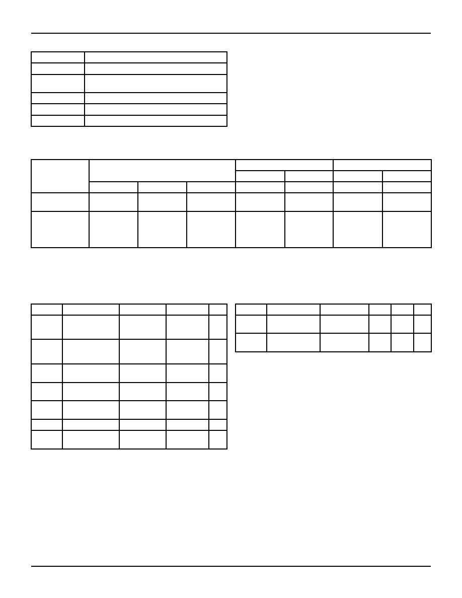
PIN DESCRIPTION
2603 tbl 06
FUNCTION TABLE
(1)
NOTE:
2603 tbl 05
1. H = HIGH Voltage Level
Z = High Impedance
L = LOW Voltage Level
NC = No Change
X = Don't Care
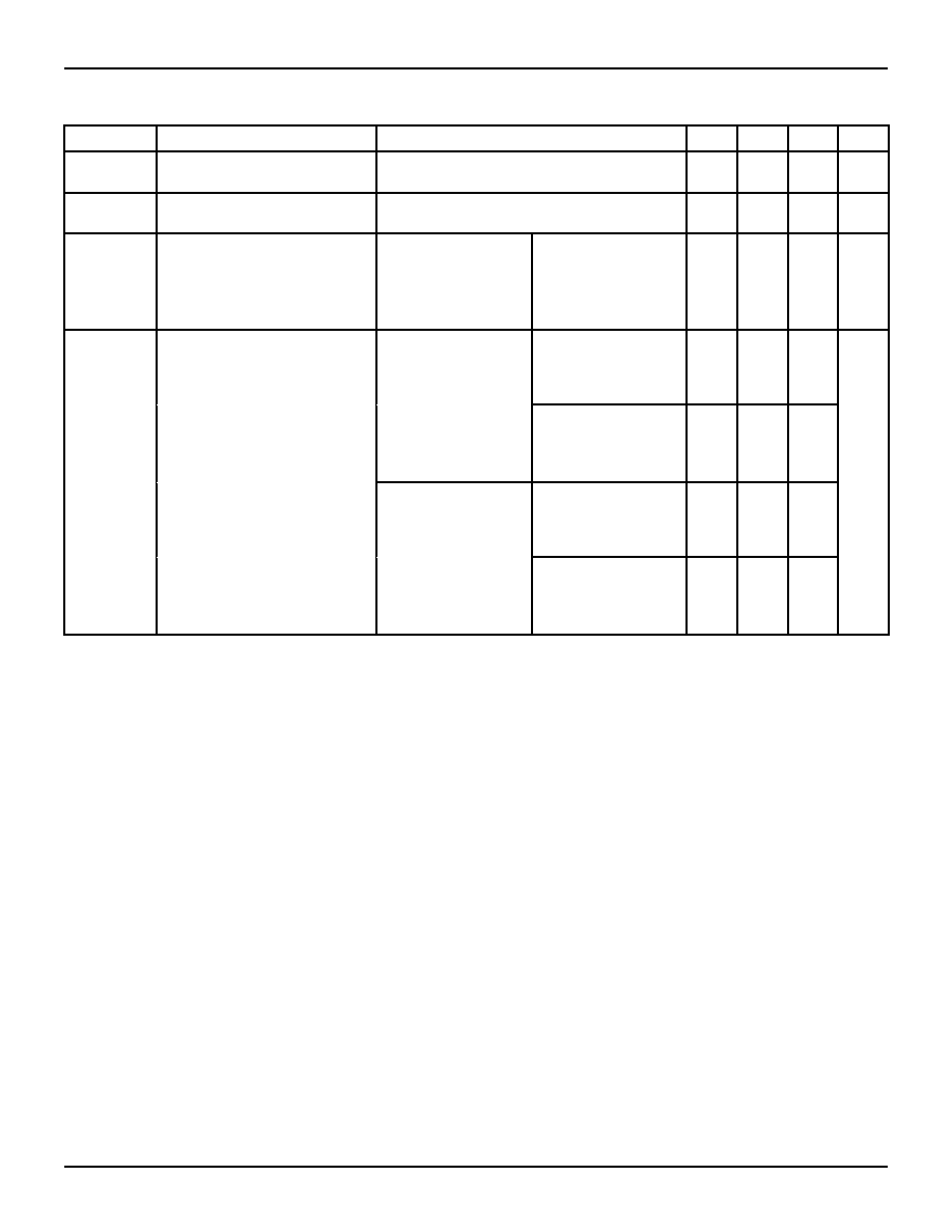
ABSOLUTE MAXIMUM RATINGS
(1)
CAPACITANCE
(T
A
= +25
∞
C, f = 1.0MHz)
NOTES:
2603 tbl 01
1. Stresses greater than those listed under ABSOLUTE MAXIMUM
RATINGS may cause permanent damage to the device. This is a stress
rating only and functional operation of the device at these or any other
conditions above those indicated in the operational sections of this
specification is not implied. Exposure to absolute maximum rating con-
ditions for extended periods may affect reliability. No terminal voltage may
exceed V
CC
by +0.5V unless otherwise noted.
2. Input and V
CC
terminals only.
3. Outputs and I/O terminals only.
Symbol
Parameter
(1)
Conditions
Typ.
Max.
Unit
C
IN
Input
Capacitance
V
IN
= 0V
6
10
pF
C
OUT
Output
Capacitance
V
OUT
= 0V
8
12
pF
NOTE:
2603 tbl 02
1. This parameter is measured at characterization but not tested.
Symbol
Rating
Commercial
Military
Unit
V
TERM(2)
Terminal Voltage
with Respect to
GND
≠0.5 to +7.0
≠0.5 to +7.0
V
V
TERM(3)
Terminal Voltage
with Respect to
GND
≠0.5 to V
CC
≠0.5 to V
CC
V
T
A
Operating
Temperature
0 to +70
≠55 to +125
∞
C
T
BIAS
Temperature
Under Bias
≠55 to +125
≠65 to +135
∞
C
T
STG
Storage
Temperature
≠55 to +125
≠65 to +150
∞
C
P
T
Power Dissipation
0.5
0.5
W
I
OUT
DC Output
Current
120
120
mA
u
= LOW-to-HIGH transition
Pin Names
Description
D
N
D flip-flop data inputs.
CP
Clock Pulse for the register. Enters data on
LOW-to-HIGH transition.
O
N
3-state outputs, (true).
O
N
3-state outputs, (inverted).
OE
Active LOW 3-state Output Enable input.
FCT534
FCT374/574
Inputs
Outputs
Internal
Outputs
Internal
Function
OE
OE
CP
D
N
O
O
N
Q
N
O
N
Q
Q
N
Hi-Z
H
H
L
H
X
X
Z
Z
NC
NC
Z
Z
NC
NC
Load Register
L
L
H
H
u
u
u
u
L
H
L
H
H
L
Z
Z
L
H
L
H
L
H
Z
Z
H
L
H
L
7.13
4
IDT54/74FCT374/534/574/A/C
FAST CMOS OCTAL D REGISTERS (3-STATE)
MILITARY AND COMMERCIAL TEMPERATURE RANGES
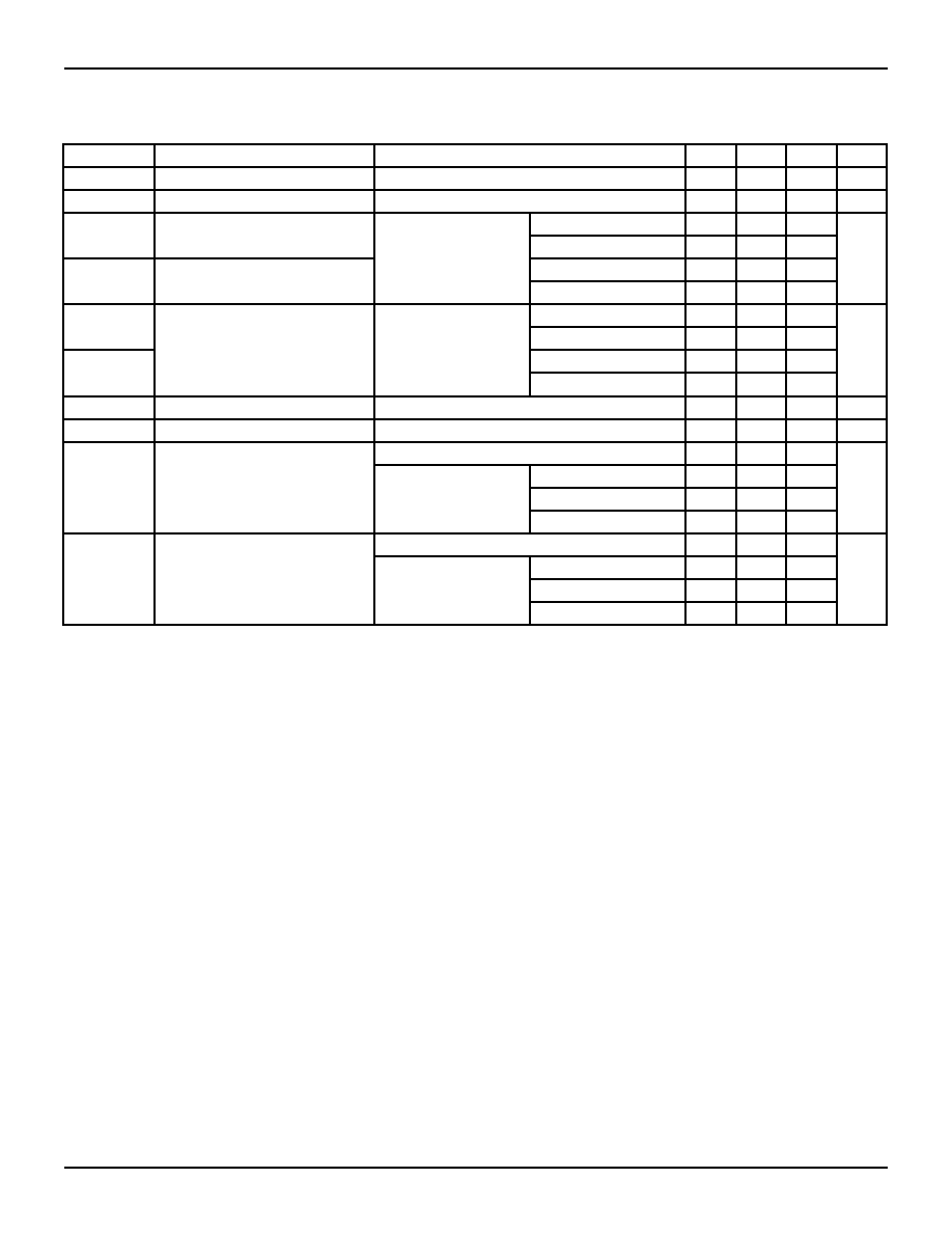
DC ELECTRICAL CHARACTERISTICS OVER OPERATING RANGE
Following Conditions Apply Unless Otherwise Specified: V
LC
= 0.2V; V
HC
= V
CC
≠ 0.2V
Commercial: T
A
= 0
∞
C to +70
∞
C, V
CC
= 5.0V
±
5%; Military: T
A
= ≠55
∞
C to +125
∞
C, V
CC
= 5.0V
±
10%
NOTES:
2603 tbl 03
1. For conditions shown as Max. or Min., use appropriate value specified under Electrical Characteristics for the applicable device type.
2. Typical values are at V
CC
= 5.0V, +25
∞
C ambient and maximum loading.
3. Not more than one output should be shorted at one time. Duration of the short circuit test should not exceed one second.
4. This parameter is guaranteed but not tested.
Symbol
Parameter
Test Conditions
(1)
Min.
Typ.
(2)
Max.
Unit
V
IH
Input HIGH Level
Guaranteed Logic HIGH Level
2.0
--
--
V
V
IL
Input LOW Level
Guaranteed Logic LOW Level
--
--
0.8
V
I
I H
Input HIGH Current
V
CC
= Max.
V
I
= V
CC
--
--
5
µ
A
V
I
= 2.7V
--
--
5
(4)
I
I L
Input LOW Current
V
I
= 0.5V
--
--
≠5
(4)
V
I
= GND
--
--
≠5
I
OZH
Off State (High Impedance)
V
CC
= Max.
V
O
= V
CC
--
--
10
µ
A
Output Current
V
O
= 2.7V
--
--
10
(4)
I
OZL
V
O
= 0.5V
--
--
≠10
(4)
V
O
= GND
--
--
≠10
V
IK
Clamp Diode Voltage
V
CC
= Min., I
N
= ≠18mA
--
≠0.7
≠1.2
V
I
OS
Short Circuit Current
V
CC
= Max.
(3)
, V
O
= GND
≠60
≠120
--
mA
V
OH
Output HIGH Voltage
V
CC
= 3V, V
IN
= V
LC
or V
HC
, I
OH
= ≠32
µ
A
V
HC
V
CC
--
V
V
CC
= Min.
I
OH
= ≠300
µ
A
V
HC
V
CC
--
V
IN
= V
IH
or V
IL
I
OH
= ≠12mA MIL.
2.4
4.3
--
I
OH
= ≠15mA COM'L.
2.4
4.3
--
V
OL
Output LOW Voltage
V
CC
= 3V, V
IN
= V
LC
or V
HC
, I
OL
= 300
µ
A
--
GND
V
LC
V
V
CC
= Min.
I
OL
= 300
µ
A
--
GND
V
LC(4)
V
IN
= V
IH
or V
IL
I
OL
= 32mA MIL.
--
0.3
0.5
I
OL
= 48mA COM'L.
--
0.3
0.5
IDT54/74FCT374/534/574/A/C
FAST CMOS OCTAL D REGISTERS (3-STATE)
MILITARY AND COMMERCIAL TEMPERATURE RANGES
7.13
5
POWER SUPPLY CHARACTERISTICS
V
LC
= 0.2V; V
HC
= V
CC
≠ 0.2V
NOTES:
2603 tbl 04
1. For conditions shown as Max. or Min., use appropriate value specified under Electrical Characteristics for the applicable device type.
2. Typical values are at V
CC
= 5.0V, +25
∞
C ambient.
3. Per TTL driven input (V
IN
= 3.4V); all other inputs at V
CC
or GND.
4. This parameter is not directly testable, but is derived for use in Total Power Supply Calculations.
5. Values for these conditions are examples of the I
CC
formula. These limits are guaranteed but not tested.
6. I
C
= I
QUIESCENT
+ I
INPUTS
+ I
DYNAMIC
I
C
= I
CC
+
I
CC
D
H
N
T
+ I
CCD
(f
CP
/2 + f
i
N
i
)
I
CC
= Quiescent Current
I
CC
= Power Supply Current for a TTL High Input (V
IN
= 3.4V)
D
H
= Duty Cycle for TTL Inputs High
N
T
= Number of TTL Inputs at D
H
I
CCD
= Dynamic Current Caused by an Input Transition Pair (HLH or LHL)
f
CP
= Clock Frequency for Register Devices (Zero for Non-Register Devices)
fi = Input Frequency
N
i
= Number of Inputs at f
i
All currents are in milliamps and all frequencies are in megahertz.
Symbol
Parameter
Test Conditions
(1)
Min.
Typ.
(2)
Max.
Unit
I
CC
Quiescent Power Supply Current
V
CC
= Max.
V
IN
V
HC
; V
IN
V
LC
--
0.2
1.5
mA
I
CC
Quiescent Power Supply Current
TTL Inputs HIGH
V
CC
= Max.
V
IN
= 3.4V
(3)
--
0.5
2.0
mA
I
CCD
Dynamic Power Supply
Current
(4)
V
CC
= Max.
Outputs Open
OE
= GND
One Input Toggling
50% Duty Cycle
V
IN
V
HC
V
IN
V
LC
--
0.15
0.25
mA/
MHz
I
C
Total Power Supply Current
(6)
V
CC
= Max.
Outputs Open
f
CP
= 10MHz
50% Duty Cycle
V
IN
V
HC
V
IN
V
LC
(FCT)
--
1.7
4.0
mA
OE
= GND
fi = 5MHz
50% Duty Cycle
One Bit Toggling
V
IN
= 3.4V
V
IN
= GND
--
2.2
6.0
V
CC
= Max.
Outputs Open
f
CP
= 10MHz
50% Duty Cycle
V
IN
V
HC
V
IN
V
LC
(FCT)
--
4.0
7.8
(5)
OE
= GND
Eight Bits Toggling
fi = 2.5MHz
50% Duty Cycle
V
IN
= 3.4V
V
IN
= GND
--
6.2
16.8
(5)