Integrated Device Technology, Inc.
DESCRIPTION:
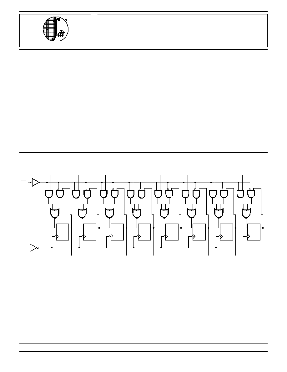
The IDT54/74FCT377T/AT/CT/DT are octal D flip-flops built
using an advanced dual metal CMOS technology. The IDT54/
74FCT377T/AT/CT/DT have eight edge-triggered, D-type flip-
flops with individual D inputs and O outputs. The common
buffered Clock (CP) input loads all flip-flops simultaneously
when the Clock Enable (
CE
) is LOW. The register is fully
edge-triggered. The state of each D input, one set-up time
before the LOW-to-HIGH clock transition, is transferred to the
corresponding flip-flop's O output. The
CE
input must be
stable only one set-up time prior to the LOW-to-HIGH transi-
tion for predictable operation.
IDT54/74FCT377T/AT/CT/DT
FAST CMOS
OCTAL D FLIP-FLOP
WITH CLOCK ENABLE
MILITARY AND COMMERCIAL TEMPERATURE RANGES
APRIL 1995
©
1995 Integrated Device Technology, Inc.
6.14
DSC-4200/3
1
The IDT logo is a registered trademark of Integrated Device Technology, Inc.
FEATURES:
∑ Std., A, C and D speed grades
∑ Low input and output leakage
1
µ
A (max.)
∑ CMOS power levels
∑ True TTL input and output compatibility
≠ V
OH
= 3.3V (typ.)
≠ V
OL
= 0.3V (typ.)
∑ High drive outputs (-15mA I
OH
, 48mA I
OL
)
∑ Power off disable outputs permit "live insertion"
∑ Meets or exceeds JEDEC standard 18 specifications
∑ Product available in Radiation Tolerant and Radiation
Enhanced versions
∑ Military product compliant to MIL-STD-883, Class B
and DESC listed (dual marked)
∑ Available in DIP, SOIC, QSOP, CERPACK and LCC
packages
2630 drw 01
CE
CP
D
CP
Q
D
0
O
0
D
CP
Q
D
1
O
1
D
CP
Q
D
2
O
2
D
CP
Q
D
3
O
3
D
CP
Q
D
4
O
4
D
CP
Q
D
5
O
5
D
CP
Q
D
6
O
6
D
CP
Q
D
7
O
7
FUNCTIONAL BLOCK DIAGRAM

6.14
2
IDT54/74FCT377T/AT/CT/DT
FAST CMOS OCTAL D FLIP-FLOP WITH CLOCK ENABLE
MILITARY AND COMMERCIAL TEMPERATURE RANGES
PIN CONFIGURATIONS
DIP/SOIC/QSOP/CERPACK
TOP VIEW
LCC
TOP VIEW
PIN DESCRIPTION
Pin Names
Description
D
0
≠ D
7
Data Inputs
CE
Clock Enable (Active LOW)
O
0
≠ O
7
Data Outputs
CP
Clock Pulse Input
2630 tbl 01
FUNCTION TABLE
(1)
Inputs
Outputs
Operating Mode
CP
CE
CE
D
O
Load "1"
l
h
H
Load "0"
l
l
L
Hold
h
X
No Change
H
H
X
No Change
NOTE:
2630 tbl 02
1. H = HIGH Voltage Level
h = HIGH Voltage Level one setup time prior to the LOW-to-HIGH
Clock Transition
L = LOW Voltage Level
l = LOW Voltage Level one setup time prior to the LOW-to-HIGH Clock
Transition
X = Don't Care
= LOW-to-HIGH Clock Transition
ABSOLUTE MAXIMUM RATINGS
(1)
CAPACITANCE
(T
A
= +25
∞
C, f = 1.0MHz)
Symbol
Parameter
(1)
Conditions
Typ.
Max. Unit
C
IN
Input
Capacitance
V
IN
= 0V
6
10
pF
C
OUT
Output
Capacitance
V
OUT
= 0V
8
12
pF
NOTE:
1. This parameter is measured at characterization but not tested.
Symbol
Rating
Commercial
Military
Unit
V
TERM(2)
Terminal Voltage
with Respect to
GND
≠0.5 to +7.0
≠0.5 to +7.0
V
V
TERM(3)
Terminal Voltage
with Respect to
GND
≠0.5 to
V
CC
+0.5
≠0.5 to
V
CC
+0.5
V
T
A
Operating
Temperature
0 to +70
≠55 to +125
∞
C
T
BIAS
Temperature
Under Bias
≠55 to +125
≠65 to +135
∞
C
T
STG
Storage
Temperature
≠55 to +125
≠65 to +150
∞
C
P
T
Power Dissipation
0.5
0.5
W
I
OUT
DC Output
Current
≠60 to +120 ≠60 to +120 mA
2630 lnk 03
2630 lnk 04
NOTES:
1. Stresses greater than those listed under ABSOLUTE MAXIMUM RAT-
INGS may cause permanent damage to the device. This is a stress rating
only and functional operation of the device at these or any other conditions
above those indicated in the operational sections of this specification is
not implied. Exposure to absolute maximum rating conditions for
extended periods may affect reliability. No terminal voltage may exceed
V
CC
by +0.5V unless otherwise noted.
2. Input and V
CC
terminals only.
3. Outputs and I/O terminals only.
2630 drw 02
5
6
7
8
9
10
D
0
D
1
O
1
1
2
3
4
20
19
18
17
16
15
14
13
Vcc
12
11
CE
D
7
O
2
D
2
D
3
O
3
CP
D
6
O
6
O
5
D
5
D
4
GND
O
4
O
0
O
7
P20-1
D20-1
SO20-2
SO20-8
&
E20-1
INDEX
15
14
18
17
16
5
6
7
8
4
L20-2
D
0
D
1
O
1
Vcc
CE
D
7
O
2
D
2
D
3
O
3
CP
D
6
O
6
O
5
D
5
D
4
GND
O
4
O
0
O
7
9 10 11 12 13
3
2
1
20 19
2630 drw 03
IDT54/74FCT377T/AT/CT/DT
FAST CMOS OCTAL D FLIP-FLOP WITH CLOCK ENABLE
MILITARY AND COMMERCIAL TEMPERATURE RANGES
6.14
3
DC ELECTRICAL CHARACTERISTICS OVER OPERATING RANGE
Following Conditions Apply Unless Otherwise Specified:
Commercial: T
A
= 0
∞
C to +70
∞
C, V
CC
= 5.0V
±
5%; Military: T
A
= ≠55
∞
C to +125
∞
C, V
CC
= 5.0V
±
10%
Symbol
Parameter
Test Conditions
(1)
Min.
Typ.
(2)
Max.
Unit
V
IH
Input HIGH Level
Guaranteed Logic HIGH Level
2.0
--
--
V
V
IL
Input LOW Level
Guaranteed Logic LOW Level
--
--
0.8
V
I
IH
Input HIGH Current
(4)
V
CC
= Max.
V
I
= 2.7V
--
--
±
1
µ
A
I
IL
Input LOW Current
(4)
V
CC
= Max.
V
I
= 0.5V
--
--
±
1
µ
A
I
I
Input HIGH Current
(4)
V
CC
= Max., V
I
= V
CC
(Max.)
--
--
±
1
µ
A
V
IK
Clamp Diode Voltage
V
CC
= Min., I
N
= ≠18mA
--
≠0.7
≠1.2
V
I
OS
Short Circuit Current
V
CC
= Max.
(3)
, V
O
= GND
≠60
≠120
≠225
mA
V
OH
Output HIGH Voltage
V
CC
= Min.
I
OH
= ≠6mA MIL.
2.4
3.3
--
V
V
IN
= V
IH
or V
IL
I
OH
= ≠8mA COM'L.
I
OH
= ≠12mA MIL.
2.0
3.0
--
V
I
OH
= ≠15mA COM'L.
V
OL
Output LOW Voltage
V
CC
= Min.
I
OL
= 32mA MIL.
--
0.3
0.5
V
V
IN
= V
IH
or V
IL
I
OL
= 48mA COM'L.
I
OFF
Input/Output Power Off
V
CC
= 0V, V
IN
or V
O
4.5V
--
--
±
1
µ
A
Leakage
(5)
V
H
Input Hysteresis
--
--
200
--
mV
I
CC
Quiescent Power
V
CC
= Max.
--
0.01
1
mA
Supply Current
V
IN
= GND or V
CC
NOTES:
2630 tbl 05
1. For conditions shown as Max. or Min., use appropriate value specified under Electrical Characteristics for the applicable device type.
2. Typical values are at V
CC
= 5.0V, +25
∞
C ambient.
3. Not more than one output should be shorted at one time. Duration of the short circuit test should not exceed one second.
4. The test limit for this parameter is
±
5
µ
A at T
A
= -55
∞
C.
5. This parameter is guaranted but not tested.
6.14
4
IDT54/74FCT377T/AT/CT/DT
FAST CMOS OCTAL D FLIP-FLOP WITH CLOCK ENABLE
MILITARY AND COMMERCIAL TEMPERATURE RANGES
POWER SUPPLY CHARACTERISTICS
Symbol
Parameter
Test Conditions
(1)
Min.
Typ.
(2)
Max.
Unit
I
CC
Quiescent Power Supply
V
CC
= Max.
--
0.5
2.0
mA
Current TTL Inputs HIGH
V
IN
= 3.4V
(3)
I
CCD
Dynamic Power Supply
V
CC
= Max., Outputs Open
V
IN
= V
CC
--
0.15
0.25
mA/
Current
(4)
CE
= GND
V
IN
= GND
MHz
One Input Toggling
50% Duty Cycle
I
C
Total Power Supply
V
CC
= Max., Outputs Open
V
IN
= V
CC
--
1.5
3.5
mA
Current
(6)
f
CP
= 10MHz
V
IN
= GND
CE
= GND
V
IN
= 3.4V
--
2.0
5.5
One Bit Toggling
V
IN
= GND
f
i
= 5MHz
50% Duty Cycle
V
CC
= Max., Outputs Open
V
IN
= V
CC
--
3.8
7.3
(5)
f
CP
= 10MHz, 50% Duty Cycle
V
IN
= GND
CE
= GND
V
IN
= 3.4V
--
6.0
16.3
(5)
Eight Bits Toggling
V
IN
= GND
f
i
= 2.5MHz
50% Duty Cycle
NOTES:
1. For conditions shown as Max. or Min., use appropriate value specified under Electrical Characteristics for the applicable device type.
2. Typical values are at V
CC
= 5.0V, +25
∞
C ambient.
3. Per TTL driven input (V
IN
= 3.4V). All other inputs at V
CC
or GND.
4. This parameter is not directly testable, but is derived for use in Total Power Supply Calculations.
5. Values for these conditions are examples of the I
CC
formula. These limits are guaranteed but not tested.
6. I
C
= I
QUIESCENT
+ I
INPUTS
+ I
DYNAMIC
I
C
= I
CC
+
I
CC
D
H
N
T
+ I
CCD
(f
CP/
2 + f
i
N
i
)
I
CC
= Quiescent Current
I
CC
= Power Supply Current for a TTL High Input (V
IN
= 3.4V)
D
H
= Duty Cycle for TTL Inputs High
N
T
= Number of TTL Inputs at D
H
I
CCD
= Dynamic Current Caused by an Input Transition Pair (HLH or LHL)
f
CP
= Clock Frequency for Register Devices (Zero for Non-Register Devices)
f
i
= Input Frequency
N
i
= Number of Inputs at f
i
All currents are in milliamps and all frequencies are in megahertz.
2639 tbl 05
IDT54/74FCT377T/AT/CT/DT
FAST CMOS OCTAL D FLIP-FLOP WITH CLOCK ENABLE
MILITARY AND COMMERCIAL TEMPERATURE RANGES
6.14
5
SWITCHING CHARACTERISTICS OVER OPERATING RANGE
NOTES:
2630 tbl 07
1. See test circuit and waveforms.
2. Minimum limits are guaranteed but not tested on Propagation Delays.
2630 tbl 06
IDT54/74FCT377T
FCT54/74FCT377AT
Com'l.
Mil.
Com'l.
Mil.
Symbol
Parameter
Condition
(1)
Min.
(2)
Max.
Min.
(2)
Max.
Min.
(2)
Max.
Min.
(2)
Max.
Unit
t
PLH
t
PHL
Propagation Delay
CP to On
C
L
= 50pF
R
L
= 500
2.0
13.0
2.0
15.0
2.0
7.2
2.0
8.3
ns
t
SU
Set-Up Time HIGH or LOW
Dn to CP
2.5
--
3.0
--
2.0
--
2.0
--
ns
t
H
Hold Time HIGH or LOW
Dn to CP
2.0
--
2.5
--
1.5
--
1.5
--
ns
t
SU
Set-Up Time HIGH or LOW
CE
to CP
4.0
--
4.0
--
3.5
--
3.5
--
ns
t
H
Hold Time HIGH or LOW
CE
to CP
1.5
--
1.5
--
1.5
--
1.5
--
ns
t
W
Clock Pulse Width,
HIGH or LOW
7.0
--
7.0
--
6.0
--
7.0
--
ns
IDT54/74FCT377CT
FCT54/74FCT377DT
Com'l.
Mil.
Com'l.
Mil.
Symbol
Parameter
Condition
(1)
Min.
(2)
Max.
Min.
(2)
Max.
Min.
(2)
Max.
Min.
(2)
Max.
Unit
t
PLH
t
PHL
Propagation Delay
CP to On
C
L
= 50pF
R
L
= 500
2.0
5.2
2.0
5.5
2.0
4.4
--
--
ns
t
SU
Set-Up Time HIGH or LOW
Dn to CP
2.0
--
2.0
--
2.0
--
--
--
ns
t
H
Hold Time HIGH or LOW
Dn to CP
1.5
--
1.5
--
1.0
--
--
--
ns
t
SU
Set-Up Time HIGH or LOW
CE
to CP
3.5
--
3.5
--
3.0
--
--
--
ns
t
H
Hold Time HIGH or LOW
CE
to CP
1.5
--
1.5
--
0.0
--
--
--
ns
t
W
Clock Pulse Width,
HIGH or LOW
6.0
--
7.0
--
3.0
--
--
--
ns