Integrated Device Technology, Inc.
IDT54/74FCT3827A/B
3.3V CMOS 10-BIT
BUFFERS
The IDT logo is a registered trademark of Integrated Device Technology, Inc.
1
MILITARY AND COMMERCIAL TEMPERATURE RANGES
AUGUST 1995
©
1995 Integrated Device Technology, Inc.
8.15
DSC-4651/-
D
0
D
1
D
2
D
3
D
4
D
5
D
6
D
7
D
8
D
9
OE
1
OE
2
Y
0
Y
1
Y
2
Y
3
Y
4
Y
5
Y
6
Y
7
Y
8
Y
9
FUNCTIONAL BLOCK DIAGRAM
3092 drw 01
FEATURES:
∑ 0.5 MICRON CMOS Technology
∑ ESD > 2000V per MIL-STD-883, Method 3015;
> 200V using machine model (C = 200pF, R = 0)
∑ 25 mil Center SSOP Packages
∑ Extended commercial range of -40
∞
C to +85
∞
C
∑ V
CC
= 3.3V
±
0.3V, Normal Range or
V
CC
= 2.7V to 3.6V, Extended Range
∑ CMOS power levels (0.4
µ
W typ. static)
∑ Rail-to-Rail output swing for increased noise margin
∑ Military product compliant to MIL-STD-883, Class B
DESCRIPTION:
The FCT3827A/B 10-bit bus drivers are built using an
advanced dual metal CMOS technology. These high speed,
low power buffers are ideal for high-performance bus interface
buffering for wide data/address paths or buses carrying parity.
The 10-bit buffers have NAND-ed output enables for maxi-
mum control flexibility.
All of the FCT3827 high performance interface compo-
nents are designed for high-capacitance load drive capability,
while providing low-capacitance bus loading at both inputs
and outputs.
IDT54/74FCT3827A/B
3.3V CMOS OCTAL BUFFERS
MILITARY AND COMMERCIAL TEMPERATURE RANGES
8.15
2
DIP/SOIC/SSOP/QSOP
TOP VIEW
PIN CONFIGURATIONS
3092 drw 02
PIN DESCRIPTION
3092 tbl 01
ABSOLUTE MAXIMUM RATINGS
(1)
Symbol
Rating
Commercial
Military
Unit
V
TERM(2)
Terminal Voltage
with Respect to
GND
≠0.5 to +4.6
≠0.5 to +4.6
V
V
TERM(3)
Terminal Voltage
with Respect to
GND
≠0.5 to +7.0
≠0.5 to +7.0
V
V
TERM(4)
Terminal Voltage
with Respect to
GND
≠0.5 to
V
CC
+ 0.5
≠0.5 to
V
CC
+ 0.5
V
T
A
Operating
Temperature
≠40 to +85
≠55 to +125
∞
C
T
BIAS
Temperature
Under Bias
≠55 to +125
≠65 to +135
∞
C
T
STG
Storage
Temperature
≠55 to +125
≠65 to +150
∞
C
P
T
Power Dissipation
1.0
1.0
W
I
OUT
DC Output
Current
≠60 to +60 ≠60 to +60 mA
3092 lnk 03
3092 tbl 02
CAPACITANCE
(T
A
= +25
∞
C, f = 1.0MHz)
NOTE:
1. This parameter is measured at characterization but not tested.
3092 lnk 04
Symbol
Parameter
(1)
Conditions
Typ.
Max.
Unit
C
IN
Input
Capacitance
V
IN
= 0V
3.5
6.0
pF
C
OUT
Output
Capacitance
V
OUT
= 0V
4.0
8.0
pF
Names
I/O
Description
OE
I
I
When both are LOW the outputs are
enabled. When either one or both are
HIGH the outputs are High Z.
D
I
I
10-bit data input.
Y
I
O
10-bit data output.
Inputs
Output
OE
OE
1
OE
OE
2
D
I
Y
I
Function
L
L
L
L
L
H
L
H
Transparent
H
X
X
H
X
X
Z
Z
Three-State
OE
1
D
0
D
1
D
2
D
3
D
4
D
5
D
6
D
7
Y
0
Y
1
Y
2
Y
3
Y
4
Y
6
Y
5
Y
7
V
CC
1
2
3
4
5
6
7
8
9
10
13
14
15
16
17
18
19
20
P24-1
D24-1
SO24-2
SO24-7
&
SO24-8
11
12
21
22
23
24
D
8
D
9
Y
8
Y
9
OE
2
GND
FUNCTION TABLE
(1)
NOTE:
1. H = HIGH Voltage Level
X = Don't Care
L = LOW Voltage Level
Z = High Impedance
NOTES:
1. Stresses greater than those listed under ABSOLUTE MAXIMUM RAT-
INGS may cause permanent damage to the device. This is a stress rating
only and functional operation of the device at these or any other conditions
above those indicated in the operational sections of this specification is
not implied. Exposure to absolute maximum rating conditions for ex-
tended periods may affect reliability.
2. Vcc terminals.
3. Input terminals.
4. Output and I/O terminals.
IDT54/74FCT3827A/B
3.3V CMOS OCTAL BUFFERS
MILITARY AND COMMERCIAL TEMPERATURE RANGES
8.15
3
DC ELECTRICAL CHARACTERISTICS OVER OPERATING RANGE
Following Conditions Apply Unless Otherwise Specified:
Commercial: T
A
= ≠40
∞
C to +85
∞
C, V
CC
= 2.7V to 3.6V; Military: T
A
= ≠55
∞
C to +125
∞
C, V
CC
= 2.7V to 3.6V
Symbol
Parameter
Test Conditions
(1)
Min.
Typ.
(2)
Max.
Unit
V
IH
Input HIGH Level (Input pins)
Guaranteed Logic HIGH Level
2.0
--
5.5
V
Input HIGH Level (I/O pins)
2.0
--
V
CC
+0.5
V
IL
Input LOW Level
Guaranteed Logic LOW Level
≠0.5
--
0.8
V
(Input and I/O pins)
I
I H
Input HIGH Current (Input pins)
(6)
V
CC
= Max.
V
I
= 5.5V
--
--
±
1
µ
A
Input HIGH Current (I/O pins)
(6)
V
I
= V
CC
--
--
±
1
I
I L
Input LOW Current (Input pins)
(6)
V
I
= GND
--
--
±
1
Input LOW Current (I/O pins)
(6)
V
I
= GND
--
--
±
1
I
OZH
High Impedance Output Current
V
CC
= Max.
V
O
= V
CC
--
--
±
1
µ
A
I
OZL
(3-State Output pins)
(6)
V
O
= GND
--
--
±
1
V
IK
Clamp Diode Voltage
V
CC
= Min., I
IN
= ≠18mA
--
≠
0.7
≠
1.2
V
I
ODH
Output HIGH Current
V
CC
= 3.3V, V
IN
= V
IH
or V
IL,
V
O
= 1.5V
(3)
≠36
≠60
≠110
mA
I
ODL
Output LOW Current
V
CC
= 3.3V, V
IN
= V
IH
or V
IL,
V
O
= 1.5V
(3)
50
90
200
mA
V
OH
Output HIGH Voltage
V
CC
= Min.
I
OH
= ≠0.1mA
V
CC
≠
0.2
--
--
V
V
IN
= V
IH
or V
IL
I
OH
= ≠3mA
2.4
3.0
--
V
CC
= 3.0V
V
IN
= V
IH
or V
IL
I
OH
= ≠6mA MIL.
I
OH
= ≠8mA COM'L.
2.4
(5)
3.0
--
V
OL
Output LOW Voltage
V
CC
= Min.
I
OL
= 0.1mA
--
--
0.2
V
V
IN
= V
IH
or V
IL
I
OL
= 16mA
--
0.2
0.4
I
OL
= 24mA
--
0.3
0.55
V
CC
= 3.0V
V
IN
= V
IH
or V
IL
I
OL
= 24mA
--
0.3
0.50
I
OS
Short Circuit Current
(4)
V
CC
= Max., V
O
= GND
(3)
≠60
≠
135
≠240
mA
V
H
Input Hysteresis
--
--
150
--
mV
I
CCL
I
CCH
Quiescent Power Supply Current
V
CC
= Max.,
V
IN
= GND or V
CC
COM'L.
--
0.1
10
µ
A
I
CCZ
MIL.
--
0.1
100
NOTES:
1. For conditions shown as Max. or Min., use appropriate value specified under Electrical Characteristics for the applicable device type.
2. Typical values are at Vcc = 3.3V, +25
∞
C ambient.
3. Not more than one output should be tested at one time. Duration of the test should not exceed one second.
4. This parameter is guaranteed but not tested.
5. V
OH
= V
CC
≠0.6V at rated current.
6. The test limits for this parameter is
±
5
µ
A at T
A
= ≠55
∞
C.
3092 lnk 05
IDT54/74FCT3827A/B
3.3V CMOS OCTAL BUFFERS
MILITARY AND COMMERCIAL TEMPERATURE RANGES
8.15
4
POWER SUPPLY CHARACTERISTICS
NOTES:
1. For conditions shown as max. or min., use appropriate value specified under Electrical Characteristics for the applicable device type.
2. Typical values are at V
CC
= 3.3V, +25
∞
C ambient.
3. Per TTL driven input; all other inputs at V
CC
or GND.
4. This parameter is not directly testable, but is derived for use in Total Power Supply Calculations.
5. Values for these conditions are examples of the I
CC
formula. These limits are guaranteed but not tested.
6. I
C
= I
QUIESCENT
+ I
INPUTS
+ I
DYNAMIC
I
C
= I
CC
+
I
CC
D
H
N
T
+ I
CCD
(f
CP
N
CP
/2 + fiNi)
I
CC
= Quiescent Current (I
CCL,
I
CCH
and
I
CCZ
)
I
CC
= Power Supply Current for a TTL High Input
D
H
= Duty Cycle for TTL Inputs High
N
T
= Number of TTL Inputs at D
H
I
CCD
= Dynamic Current Caused by an Input Transition Pair (HLH or LHL)
f
CP
= Clock Frequency for Register Devices (Zero for Non-Register Devices)
N
CP
= Number of Clock Inputs at f
CP
f
i
= Input Frequency
N
i
= Number of Inputs at fi
3092 tbl 06
Symbol
Parameter
Test Conditions
(1)
Min.
Typ.
(2)
Max.
Unit
I
CC
Quiescent Power Supply Current
V
CC
= Max.
V
IN
= V
CC
≠0.6V
(3)
--
2.0
30
µ
A
I
CCD
Dynamic Power Supply Current
(4)
V
CC
= Max.
Outputs Open
OE
1
=
OE
2
= GND
One Input Toggling
50% Duty Cycle
V
IN
= V
CC
V
IN
= GND
--
60
85
µ
A/
MHz
I
C
Total Power Supply Current
(6)
V
CC
= Max.
Outputs Open
fi = 10MHz
V
IN
= V
CC
V
IN
= GND
--
0.6
0.9
mA
50% Duty Cycle
OE
1
=
OE
2
= GND
One Bit Toggling
V
IN
= V
CC
≠0.6V
V
IN
= GND
--
0.6
0.9
V
CC
= Max.
Outputs Open
fi = 2.5MHz
V
IN
= V
CC
V
IN
= GND
--
1.5
2.1
(5)
50% Duty Cycle
OE
1
=
OE
2
= GND
Ten Bits Toggling
V
IN
= V
CC
≠0.6V
V
IN
= GND
--
1.5
2.3
(5)
IDT54/74FCT3827A/B
3.3V CMOS OCTAL BUFFERS
MILITARY AND COMMERCIAL TEMPERATURE RANGES
8.15
5
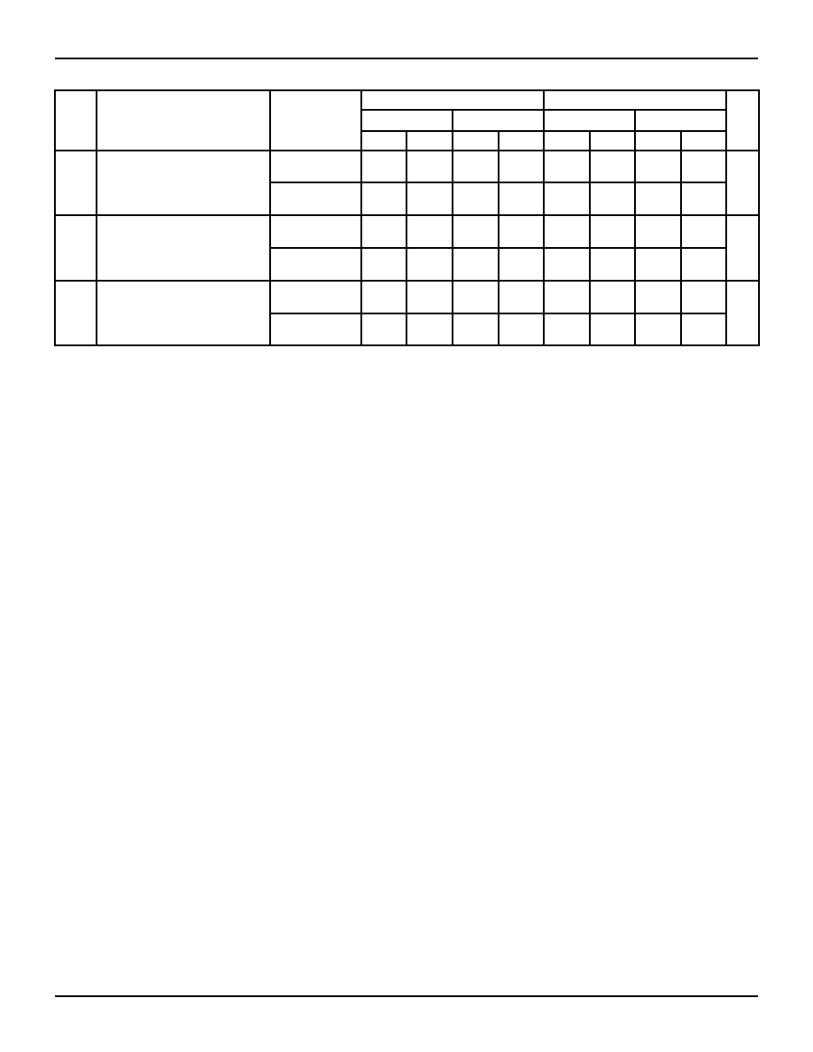
SWITCHING CHARACTERISTICS OVER OPERATING RANGE
(3)
FCT3827A
FCT3827B
Com'l.
Mil.
Com'l.
Mil.
Symbol
Parameter
Condition
(1)
Min.
(2)
Max.
Min.
(2)
Max.
Min.
(2)
Max.
Min.
(2)
Max.
Unit
t
PLH
t
PHL
Propagation Delay
D
I
to Y
I
C
L
= 50pF
R
L
= 500
1.5
8.0
1.5
9.0
1.5
5.0
1.5
6.5
ns
C
L
= 300pF
(3)
R
L
= 500
1.5
15.0
1.5
17.0
1.5
13.0
1.5
14.0
t
PZH
t
PZL
Output Enable Time
OE
I
to Y
I
C
L
= 50pF
R
L
= 500
1.5
12.0
1.5
13.0
1.5
8.0
1.5
9.0
ns
C
L
= 300pF
(3)
R
L
= 500
1.5
23.0
1.5
25.0
1.5
15.0
1.5
16.0
t
PHZ
t
PLZ
Output Disable Time
OE
I
to Y
I
C
L
= 5pF
(3)
R
L
= 500
1.5
9.0
1.5
9.0
1.5
6.0
1.5
7.0
ns
C
L
= 50pF
R
L
= 500
1.5
10.0
1.5
10.0
1.5
7.0
1.5
8.0
3092 tbl 07
NOTES:
1. See test circuit and waveforms.
2. Minimum limits are guaranteed but not tested on Propagation Delays.
3. Propagation Delays and Enable/Disable times are with V
CC
= 3.3V
±
0.3V, Normal Range. For V
CC
= 2.7V to 3.6V, Extended Range, all Propagation Delays
and Enable/Disable times should be degraded by 20%.