IDT54/74FCT388915T 70/100/133/150
3.3V LOW SKEW PLL-BASED CLOCK DRIVER
MILITARY AND COMMERCIAL TEMPERATURE RANGES
9.8
1
Integrated Device Technology, Inc.
The IDT logo is a registered trademark of Integrated Device Technology, Inc.
FEATURES:
∑ 0.5 MICRON CMOS Technology
∑ Input frequency range: 10MHz ≠ f2Q Max. spec
(FREQ_SEL = HIGH)
∑ Max. output frequency: 150MHz
∑ Pin and function compatible with FCT88915T, MC88915T
∑ 5 non-inverting outputs, one inverting output, one 2x
output, one
˜
2 output; all outputs are TTL-compatible
∑ 3-State outputs
∑ Output skew < 350ps (max.)
∑ Duty cycle distortion < 500ps (max.)
∑ Part-to-part skew: 1ns (from t
PD
max. spec)
∑ 32/≠16mA drive at CMOS output voltage levels
∑ V
CC
= 3.3V
±
0.3V
∑ Inputs can be driven by 3.3V or 5V components
∑ Available in 28 pin PLCC, LCC and SSOP packages
1
MILITARY AND COMMERCIAL TEMPERATURE RANGES
AUGUST 1995
©
1995 Integrated Device Technology, Inc.
9.8
DSC-4243/1
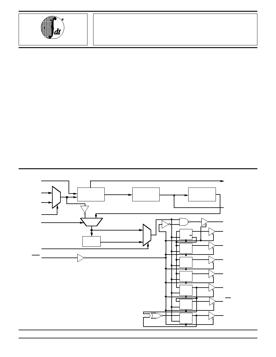
is fed back to the PLL at the FEEDBACK input resulting in
essentially zero delay across the device. The PLL consists of
the phase/frequency detector, charge pump, loop filter and
VCO. The VCO is designed for a 2Q operating frequency
range of 40MHz to f2Q Max.
The IDT54/74FCT388915T provides 8 outputs with 350ps
skew. The
Q5
output is inverted from the Q outputs. The 2Q
runs at twice the Q frequency and Q/2 runs at half the Q
frequency.
The FREQ_SEL control provides an additional
˜
2 option in
the output path. PLL _EN allows bypassing of the PLL, which
is useful in static test modes. When PLL_EN is low, SYNC
input may be used as a test clock. In this test mode, the input
frequency is not limited to the specified range and the polarity
of outputs is complementary to that in normal operation
(PLL_EN = 1). The LOCK output attains logic HIGH when the
PLL is in steady-state phase and frequency lock. When OE/
RST
is low, all the outputs are put in high impedance state and
registers at Q,
Q
and Q/2 outputs are reset.
The IDT54/74FCT388915T requires one external loop filter
component as recommended in Figure 3.
IDT54/74FCT388915T
70/100/133/150
PRELIMINARY
3.3V LOW SKEW PLL-BASED
CMOS CLOCK DRIVER
(WITH 3-STATE)
Phase/Freq.
Detector
M
u
x
0
1
SYNC (0)
FEEDBACK
SYNC (1)
REF_SEL
PLL_EN
Mux
0
1
Divide
-By-2
(
˜
1)
(
˜
2)
1
0
M
u
x
Charge Pump
Voltage
Controlled
Oscilator
OE/RST
FREQ_SEL
2Q
Q0
Q1
Q2
Q3
Q4
Q5
Q/2
D
Q
CP
Q
R
D
Q
CP
Q
R
D
Q
CP
R
D
Q
CP
R
D
Q
CP
R
D
Q
CP
R
D
Q
CP
R
D
Q
CP
LF
LOCK
3052 drw 01
DESCRIPTION:
The IDT54/74FCT388915T uses phase-lock loop technol-
ogy to lock the frequency and phase of outputs to the input
reference clock. It provides low skew clock distribution for
high performance PCs and workstations. One of the outputs
FUNCTIONAL BLOCK DIAGRAM

IDT54/74FCT388915T 70/100/133/150
3.3V LOW SKEW PLL-BASED CMOS CLOCK DRIVER
MILITARY AND COMMERCIAL TEMPERATURE RANGES
9.8
2
PIN CONFIGURATIONS
PLCC/LCC
TOP VIEW
PIN DESCRIPTION
SSOP
TOP VIEW
3052 drw 03
5
6
7
8
9
10
V
CC
OE/RST
FEEDBACK
1
2
3
4
20
19
18
17
16
15
14
13
Q4
12
11
GND
Q/2
REF_SEL
SYNC(0)
V
CC
(AN)
LF
V
CC
GND
Q3
V
CC
Q2
GND
GND(AN)
LOCK
Q5
2Q
SO28-7
21
22
23
24
SYNC(1)
FREQ_SEL
GND
Q0
V
CC
Q1
GND
PLL_EN
25
26
27
28
OE/RST
V
CC
Q5
GND
Q4
V
CC
2Q
Q/2
GND
Q3
V
CC
Q2
GND
LOCK
PLL_EN
GND
Q1
V
CC
Q0
GND
FREQ_SEL
FEEDBK
REF_SEL
SYNC(0)
V
CC
(AN)
LF
GND(AN)
SYNC(1)
28
4
3
2
1
27
26
25
24
23
22
21
20
19
5
6
7
8
9
10
11
12
13
14
15
16
17
18
J28-1,
L28-1
3052 drw 02
Pin Name
I/O
Description
SYNC(0)
I
Reference clock input.
SYNC(1)
I
Reference clock input.
REF_SEL
I
Chooses reference between SYNC (0) & SYNC (1). (Refer to functional block diagram).
FREQ_SEL
I
Selects between
˜
1 and
˜
2 frequency options. (Refer to functional block diagram).
FEEDBACK
I
Feedback input to phase detector.
LF
I
Input for external loop filter connection.
Q0-Q4
O
Clock output.
Q5
O
Inverted clock output.
2Q
O
Clock output (2 x Q frequency).
Q/2
O
Clock output (Q frequency
˜
2).
LOCK
O
Indicates phase lock has been achieved (HIGH when locked).
OE/
RST
I
Asynchronous reset (active LOW) and output enable (active HIGH). When HIGH, outputs are
enabled. When LOW, outputs are in HIGH impedance.
PLL_EN
I
Disables phase-lock for low frequency testing. (Refer to functional block diagram).
3052 tbl 01
IDT54/74FCT388915T 70/100/133/150
3.3V LOW SKEW PLL-BASED CLOCK DRIVER
MILITARY AND COMMERCIAL TEMPERATURE RANGES
9.8
3
ABSOLUTE MAXIMUM RATINGS
(1)
CAPACITANCE
(T
A
= +25
∞
C, f = 1.0MHz)
DC ELECTRICAL CHARACTERISTICS OVER OPERATING RANGE
Following Conditions Apply Unless Otherwise Specified:
Commercial: T
A
= 0
∞
C to 70
∞
C, V
CC
= 3.3V
±
0.3V
Symbol
Parameter
Test Conditions
(1)
Min.
Typ.
(2)
Max.
Unit
V
IH
Input HIGH Level
Guaranteed Logic HIGH Level
2.0
--
5.5
V
V
IL
Input LOW Level
Guaranteed Logic LOW Level
≠0.5
--
0.8
V
I
I H
Input HIGH Current
V
CC
= Max.
V
I
= 5.5V
--
--
±
1
µ
A
I
I L
Input LOW Current
V
I
= GND
--
--
±
1
µ
A
I
OZH
High Impedance Output Current
V
CC
= Max.
V
O
= V
CC
--
--
±
1
µ
A
I
OZL
(3-State Output Pins)
V
O
= GND
--
--
±
1
µ
A
V
IK
Clamp Diode Voltage
V
CC
= Min., I
IN
= ≠18mA
--
≠0.7
≠1.2
V
I
ODH
Output Drive Current
V
CC
= Max., V
IN
= V
IH
or V
IL
, V
O
= 1.5V
(3)
≠36
--
--
mA
I
ODL
Output Drive Current
V
CC
= Max., V
IN
= V
IH
or V
IL
, V
O
= 1.5V
(3)
50
--
--
mA
V
OH
Output HIGH Voltage
V
CC
= Min.
I
OH
= ≠16mA
2.4
(5)
3.0
--
V
V
OL
Output LOW Voltage
V
CC
= Min.
I
OL
= 32mA
--
0.3
0.5
V
V
H
Input Hysteresis
--
--
100
--
mV
I
CCL
I
CCH
I
CCZ
Quiescent Power Supply Current
V
CC
= Max., V
IN
= GND or V
CC
(Test mode)
--
2.0
4.0
mA
NOTES:
1. For conditions shown as Max. or Min., use appropriate value specified under Electrical Characteristics for the applicable device type.
2. Typical values are at V
CC
= 3.3V, +25
∞
C ambient.
3. Not more than one output should be tested at one time. Duration of the test should not exceed one second.
4. This parameter is guaranteed but not tested.
5. V
OH
= V
CC
- 0.6V at rated current.
3052 tbl 04
3052 tbl 02
NOTES:
1. Stresses greater than those listed under ABSOLUTE MAXIMUM RAT-
INGS may cause permanent damage to the device. This is a stress rating
only and functional operation of the device at these or any other conditions
above those indicated in the operational sections of this specification is
not implied. Exposure to absolute maximum rating conditions for ex-
tended periods may affect reliability.
2. Vcc terminals.
3. Input terminals.
4. Output and I/O terminals.
Symbol
Rating
Commercial
Military
Unit
V
TERM(2)
Terminal Voltage
with Respect to
GND
≠0.5 to +4.6
≠0.5 to +4.6
V
V
TERM(3)
Terminal Voltage
with Respect to
GND
≠0.5 to +7.0
≠0.5 to +7.0
V
V
TERM(4)
Terminal Voltage
with Respect to
GND
≠0.5 to V
CC
+0.5
≠0.5 to V
CC
+0.5
V
T
A
Operating
Temperature
0 to +70
≠55 to +125
∞
C
T
BIAS
Temperature
Under Bias
≠55 to +125
≠65 to +135
∞
C
T
STG
Storage
Temperature
≠55 to +125
≠65 to +150
∞
C
I
OUT
DC Output
Current
≠60 to +60 ≠60 to +60 mA
Symbol
Parameter
(1)
Conditions
Typ.
Max.
Unit
C
IN
Input
Capacitance
V
IN
= 0V
4.5
6.0
pF
C
OUT
Output
Capacitance
V
OUT
= 0V
5.5
8.0
pF
3052 lnk 03
NOTE:
1. This parameter is measured at characterization but not tested.

IDT54/74FCT388915T 70/100/133/150
3.3V LOW SKEW PLL-BASED CMOS CLOCK DRIVER
MILITARY AND COMMERCIAL TEMPERATURE RANGES
9.8
4
POWER SUPPLY CHARACTERISTICS
OUTPUT FREQUENCY SPECIFICATIONS
NOTES:
1. Note 7 in "General AC Specification Notes" and Figure 3 describes this specification and its actual limits depending on the feedback connection.
2. Maximum operating frequency is guaranteed with the part in a phase locked condition and all outputs loaded.
SYNC INPUT TIMING REQUIREMENTS
3052 tbl 06
NOTES:
1. For conditions shown as Max. or Min., use appropriate value specified under Electrical Characteristics for the applicable device type.
2. Typical values are at V
CC
= 3.3V, +25
∞
C ambient.
3. Per TTL driven input. All other inputs at V
CC
or GND.
4. This parameter is not directly testable, but is derived for use in Total Power Supply Calculations. It is derived with Q frequency as the reference.
5. Values for these conditions are examples of the I
CC
formula. These limits are guaranteed but not tested.
6. I
C
= I
QUIESCENT
+ I
INPUTS
+ I
DYNAMIC
I
C
= I
CC
+
I
CC
D
H
N
T
+ I
CCD
(f) + I
LOAD
I
CC
= Quiescent Current (I
CCL
,
I
CCH
and I
CCZ
)
I
CC
= Power Supply Current for a TTL High Input (V
IN
= 3.4V)
D
H
= Duty Cycle for TTL Inputs High
N
T
= Number of TTL Inputs at D
H
I
CCD
= Dynamic Current Caused by an Input Transition Pair (HLH or LHL)
f =2Q Frequency
I
LOAD
= Dynamic Current due to load.
3052 tbl 05
Symbol
Parameter
Min.
Max.
Unit
T
RISE/FALL
Rise/Fall Times,
SYNC inputs
(0.8V to 2.0V)
--
3.0
ns
Frequency Input Frequency,
SYNC Inputs
10.0
(1)
2Q fmax
MHz
Duty Cycle Input Duty Cycle,
SYNC Inputs
25%
75%
--
Symbol
Parameter
Test Conditions
(1)
Min.
Typ.
(2)
Max.
Unit
I
CC
Quiescent Power Supply Current
V
CC
= Max.
V
IN
= V
CC
≠0.6V
(3)
--
2.0
30
µ
A
TTL Inputs HIGH
V
IN
= V
CC
≠2.1V
(3)
I
CCD
Dynamic Power Supply
Current
(4)
V
CC
= Max.
All Outputs Open
V
IN
= V
CC
V
IN
= GND
--
0.2
0.3
mA/
MHz
C
PD
Power Dissipation Capacitance
50% Duty Cycle
--
15
25
pF
I
C
Total Power Supply Current
(6)
V
CC
= Max.
PLL_EN = 1, LOCK = 1, FEEDBACK = Q4
SYNC frequency = 50MHz. All bits loaded with
15pF
--
30
60
mA
V
CC
= Max.
PLL_EN = 1, LOCK = 1, FEEDBACK = Q4
SYNC frequency = 50MHz. All bits loaded with
50
Thevenin termination and 20pF
--
90
120
mA
3052 tbl 07
Max.
(2)
Symbol
Parameter
Min.
70
100
133
150
Unit
f2Q
Operating frequency 2Q Output
40
70
100
133
150
MHz
fQ
Operating frequency Q0-Q4,
Q
5 Outputs
20
35
50
66.7
75
MHz
fQ/2
Operating frequency Q/2 Output
10
17.5
25
33.3
37.5
MHz

IDT54/74FCT388915T 70/100/133/150
3.3V LOW SKEW PLL-BASED CLOCK DRIVER
MILITARY AND COMMERCIAL TEMPERATURE RANGES
9.8
5
Symbol
Parameter
Condition
(1)
Min.*
Max.*
Unit
t
RISE/FALL
All Outputs
Rise/Fall Time
(between 0.8V and 2.0V)
Load = 50
to
V
CC
/2, C
L
= 20pF
0.2
(2)
1.5
ns
t
PULSE WIDTH (3)
Q,
Q
, Q/2 outputs
(3)
Output Pulse Width
Q0-Q4,
Q
5, Q/2, @ 1.5V
Load = 50
to
V
CC
/2, C
L
= 20pF
0.5t
CYCLE
≠ 0.5
(5)
0.5t
CYCLE
+ 0.5
(5)
ns
t
PULSE WIDTH
2Q Output
(3)
Output Pulse Width
2Q @ 1.5V
0.5t
CYCLE
≠ 0.7
(5)
0.5t
CYCLE
+ 0.7
(5)
ns
t
PD
SYNC-FEEDBACK
(3)
SYNC input to FEEDBACK delay
(measured at SYNC0 or 1 and FEEDBACK
input pins)
Load = 50
to
V
CC
/2, C
L
= 20pF
0.1
µ
F from LF to
Analog GND
(5)
≠0.5
+0.5
ns
t
SKEW
r
(rising)
(3,4)
Output to Output Skew
between outputs 2Q, Q0-Q4,
Q/2 (rising edges only)
Load = 50
to
V
CC
/2, C
L
= 20pF
--
250
ps
t
SKEW
f
(falling)
(3,4)
Output to Output Skew
between outputs Q0-Q4 (falling edges only)
--
250
ps
t
SKEW
all
(3,4)
Output to Output Skew
2Q, Q/2, Q0-Q4 rising,
Q
5 falling
--
350
ps
t
LOCK(6)
Time required to acquire
Phase-Lock from time
SYNC input signal is received
1
(2)
10
ms
t
PZH
t
PZL
Output Enable Time
OE/
RST
(LOW-to-HIGH) to Q, 2Q, Q/2,
Q
3
(2)
14
ns
t
PHZ
t
PLZ
Output Disable Time
OE/
RST
(HIGH-to-LOW) to Q, 2Q, Q/2,
Q
3
(2)
14
ns
SWITCHING CHARACTERISTICS OVER OPERATING RANGE
GENERAL AC SPECIFICATION NOTES:
*
PRELIMINARY.
1. See test circuit and waveforms.
2. Minimum limits are guaranteed but not tested.
3. These specifications are guaranteed but not production tested.
4. Under equally loaded conditions, as specified under test conditions and at a fixed temperature and voltage.
5. t
CYCLE
= 1/frequency at which each output (Q,
Q
, Q/2 or 2Q) is expected to run.
6. With V
CC
fully powered-on and an output properly connected to the FEEDBACK pin. t
LOCK
Max. is with C1 = 0.1
µ
F, t
LOCK
Min. is with C1 = 0.01
µ
F. (Where
C1 is loop filter capacitor shown in Figure 2).
3052 tbl 08