MILITARY AND INDUSTRIAL TEMPERATURE RANGES
IDT54/74FCT541T/AT/CT
FAST CMOS OCTAL BUFFER/LINE DRIVER
1
JUNE 2002
MILITARY AND INDUSTRIAL TEMPERATURE RANGES
The IDT logo is a registered trademark of Integrated Device Technology, Inc.
© 2002 Integrated Device Technology, Inc.
DSC-5589/3
FEATURES:
∑ Std., A, and C grades
∑ Low input and output leakage
1µA (max.)
∑ CMOS power levels
∑ True TTL input and output compatibility:
≠ V
OH
= 3.3V (typ.)
≠ V
OL
= 0.3V (typ.)
∑ High Drive outputs (-15mA I
OH
, 64mA I
OL
)
∑ Meets or exceeds JEDEC standard 18 specifications
∑ Military product compliant to MIL-STD-883, Class B and DESC
listed (dual marked)
∑ Power off disable outputs permit "live insertion"
∑ Available in the following packages:
≠ Industrial: SOIC, SSOP, QSOP, TSSOP
≠ Military: CERDIP, LCC
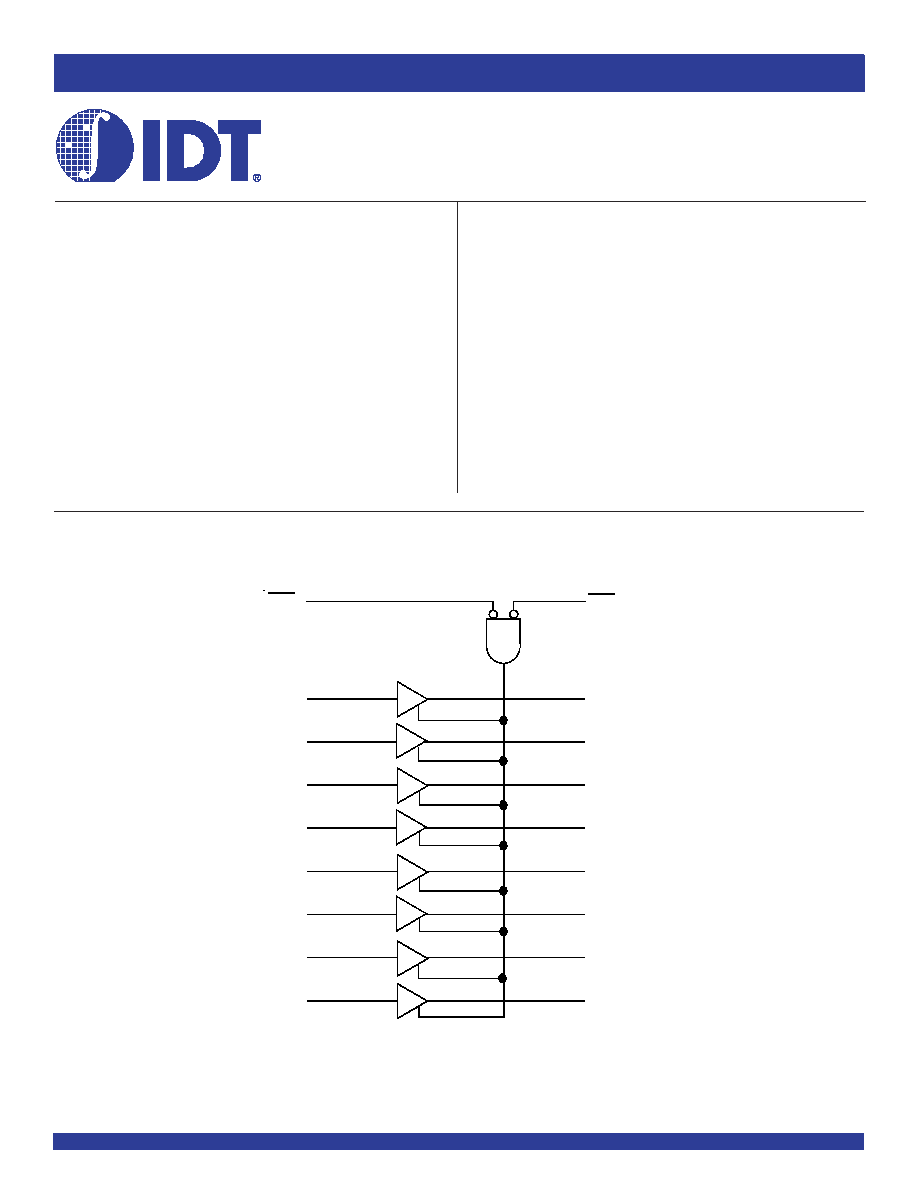
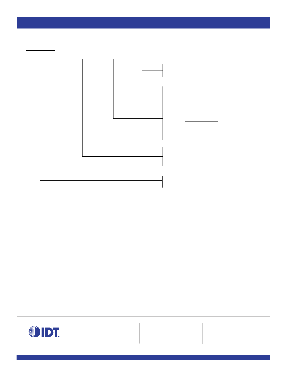
FUNCTIONAL BLOCK DIAGRAM
IDT54/74FCT541T/AT/CT
FAST CMOS OCTAL
BUFFER/LINE DRIVER
DESCRIPTION:
The IDT octal buffer/line driver is built using an advanced dual metal
CMOS technology. The FCT541T is similar in function to the FCT244T,
except that the inputs and outputs are on opposite sides of the package. This
pinout arrangement makes these devices especially useful as output ports
for microprocessors and as backplane drivers, allowing ease of layout and
greater board density.
D
0
D
2
D
3
D
4
D
5
D
6
D
7
D
1
OE
B
OE
A
O
0
O
2
O
3
O
4
O
5
O
6
O
7
O
1
MILITARY AND INDUSTRIAL TEMPERATURE RANGES
2
IDT54/74FCT541T/AT/CT
FAST CMOS OCTAL BUFFER/LINE DRIVER
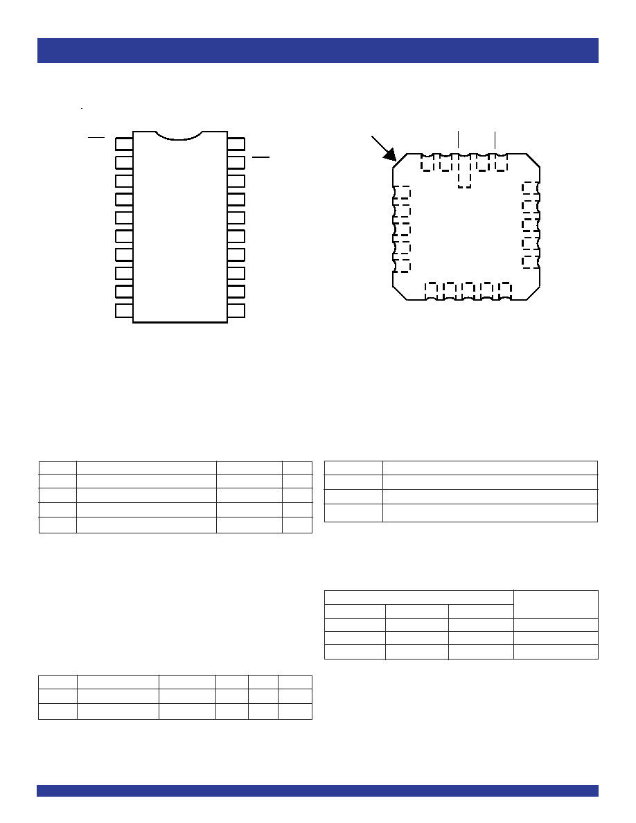
PIN CONFIGURATION
Symbol
Description
Max
Unit
V
TERM
(2)
Terminal Voltage with Respect to GND
≠0.5 to +7
V
V
TERM
(3)
Terminal Voltage with Respect to GND
≠0.5 to V
CC
+0.5
V
T
STG
Storage Temperature
≠65 to +150
∞C
I
OUT
DC Output Current
≠60 to +120
mA
ABSOLUTE MAXIMUM RATINGS
(1)
NOTES:
1. Stresses greater than those listed under ABSOLUTE MAXIMUM RATINGS may cause
permanent damage to the device. This is a stress rating only and functional operation
of the device at these or any other conditions above those indicated in the operational
sections of this specification is not implied. Exposure to absolute maximum rating
conditions for extended periods may affect reliability. No terminal voltage may exceed
Vcc by +0.5V unless otherwise noted.
2. Inputs and Vcc terminals only.
3. Output and I/O terminals only.
Pin Names
Description
OE
A
, OE
B
3-State Output Enable Inputs (Active LOW)
Dx
Inputs
Ox
Outputs
PIN DESCRIPTION
Symbol
Parameter
(1)
Conditions
Typ.
Max.
Unit
C
IN
Input Capacitance
V
IN
= 0V
6
10
pF
C
OUT
Output Capacitance
V
OUT
= 0V
8
12
pF
CAPACITANCE
(T
A
= +25∞C, F = 1.0MHz)
NOTE:
1. This parameter is measured at characterization but not tested.
NOTE:
1. H = HIGH Voltage Level
X = Don't Care
L = LOW Voltage Level
Z = High Impedance
FUNCTION TABLE
(1)
Inputs
OE
A
OE
B
D
Outputs
L
L
L
L
L
L
H
H
H
H
X
Z
CERDIP/ SOIC/ SSOP/ QSOP/ TSSOP
TOP VIEW
LCC
TOP VIEW
D
2
D
3
D
4
D
5
D
6
D
0
D
1
O
E
A
V
C
C
O
E
B
O
0
O
1
O
2
O
3
O
4
O
7
O
5
O
6
D
7
G
N
D
INDEX
D
0
D
1
D
2
D
3
D
4
D
5
D
6
D
7
GND
O
0
O
1
O
2
O
3
O
5
O
7
O
4
O
6
V
CC
1
2
3
4
5
6
7
8
9
10
11
12
13
14
15
16
17
18
19
20
OE
B
OE
A
1
2
3
4
5
6
7
8
9 10 11 12 13
14
15
16
17
18
19
20

MILITARY AND INDUSTRIAL TEMPERATURE RANGES
IDT54/74FCT541T/AT/CT
FAST CMOS OCTAL BUFFER/LINE DRIVER
3
Symbol
Parameter
Test Conditions
(1)
Min.
Typ.
(2)
Max.
Unit
V
IH
Input HIGH Level
Guaranteed Logic HIGH Level
2
--
--
V
V
IL
Input LOW Level
Guaranteed Logic LOW Level
--
--
0.8
V
I
IH
Input HIGH Current
(4)
V
CC
= Max.
V
I
= 2.7V
--
--
±1
µA
I
IL
Input LOW Current
(4)
V
CC
= Max.
V
I
= 0.5V
--
--
±1
µA
I
OZH
High Impedance Output Current
V
CC
= Max
V
O
= 2.7V
--
--
±1
µA
I
OZL
(3-State output pins)
(4)
V
O
= 0.5V
--
--
±1
I
I
Input HIGH Current
(4)
V
CC
= Max., V
I
= V
CC
(Max.)
--
--
±1
µA
V
IK
Clamp Diode Voltage
V
CC
= Min, I
IN
= -18mA
--
≠0.7
≠1.2
V
V
H
Input Hysteresis
--
--
200
--
mV
I
CC
Quiescent Power Supply Current
V
CC
= Max., V
IN
= GND or V
CC
--
0.01
1
mA
DC ELECTRICAL CHARACTERISTICS OVER OPERATING RANGE
Following Conditions Apply Unless Otherwise Specified:
Industrial: T
A
= ≠40∞C to +85∞C, V
CC
= 5.0V ±5%; Military: T
A
= ≠55∞C to +125∞C, V
CC
= 5.0V ±10%
NOTES:
1. For conditions shown as Min. or Max., use appropriate value specified under Electrical Characteristics for the applicable device type.
2. Typical values are at V
CC
= 5.0V, +25∞C ambient.
3. Not more than one output should be tested at one time. Duration of the test should not exceed one second.
4. The test limit for this parameter is ±5µA at T
A
= ≠55∞C.
Symbol
Parameter
Test Conditions
(1)
Min.
Typ.
(2)
Max.
Unit
V
OH
Output HIGH Voltage
V
CC
= Min
I
OH
= ≠6mA MIL
2.4
3.3
--
V
IN
= V
IH
or V
IL
I
OH
= ≠8mA IND
V
I
OH
= ≠12mA MIL
2
3
--
I
OH
= ≠15mA IND
V
OL
Output LOW Voltage
V
CC
= Min
I
OL
= 48mA MIL
--
0.3
0.55
V
V
IN
= V
IH
or V
IL
I
OL
= 64mA IND
I
OS
Short Circuit Current
V
CC
= Max., V
O
= GND
(3)
≠60
≠120
≠225
mA
OUTPUT DRIVE CHARACTERISTICS
MILITARY AND INDUSTRIAL TEMPERATURE RANGES
4
IDT54/74FCT541T/AT/CT
FAST CMOS OCTAL BUFFER/LINE DRIVER
Symbol
Parameter
Test Conditions
(1)
Min.
Typ.
(2)
Max.
Unit
I
CC
Quiescent Power Supply Current
V
CC
= Max.
--
0.5
2
mA
TTL Inputs HIGH
V
IN
= 3.4V
(3)
I
CCD
Dynamic Power Supply
V
CC
= Max.
V
IN
= V
CC
--
0.15
0.25
mA/
Current
(4)
Outputs Open
V
IN
= GND
MHz
OE
A
= OE
B
= GND
One Input Toggling
50% Duty Cycle
I
C
Total Power Supply Current
(6)
V
CC
= Max.
V
IN
= V
CC
--
1.5
3.5
mA
Outputs Open
V
IN
= GND
fi = 10MHz
50% Duty Cycle
V
IN
= 3.4V
--
1.8
4.5
OE
A
= OE
B
= GND
V
IN
= GND
One Bit Toggling
V
CC
= Max.
V
IN
= V
CC
--
3
6
(5)
Outputs Open
V
IN
= GND
fi = 2.5MHz
50% Duty Cycle
V
IN
= 3.4V
--
5
14
(5)
OE
A
= OE
B
= GND
V
IN
= GND
Eight Bits Toggling
NOTES:
1. For conditions shown as Min. or Max., use appropriate value specified under Electrical Characteristics for the applicable device type.
2. Typical values are at V
CC
= 5.0V, +25∞C ambient.
3. Per TTL driven input; (V
IN
= 3.4V). All other inputs at V
CC
or GND.
4. This parameter is not directly testable, but is derived for use in Total Power Supply Calculations.
5. Values for these conditions are examples of
I
CC
formula. These limits are guaranteed but not tested.
6. I
C
= I
QUIESCENT
+ I
INPUTS
+ I
DYNAMIC
I
C
= I
CC
+
I
CC
D
H
N
T
+ I
CCD
(f
CP
/2+ f
i
N
i
)
I
CC
= Quiescent Current
I
CC
= Power Supply Current for a TTL High Input (V
IN
= 3.4V)
D
H
= Duty Cycle for TTL Inputs High
N
T
= Number of TTL Inputs at D
H
I
CCD
= Dynamic Current caused by an Input Transition Pair (HLH or LHL)
f
CP
= Clock Frequency for Register Devices (Zero for Non-Register Devices)
f
i
= Output Frequency
N
i
= Number of Outputs at f
i
All currents are in milliamps and all frequencies are in megahertz.
POWER SUPPLY CHARACTERISTICS
SWITCHING CHARACTERISTICS OVER OPERATING RANGE
54FCT541T
54/74FCT541AT
54/74FCT541CT
Mil.
Ind.
Mil.
Ind.
Mil.
Symbol Parameter
Condition
(1)
Min
.(2)
Max
.
Min
.(2)
Max
.
Min
.(2)
Max
.
Min
.(2)
Max
.
Min
.(2)
Max
.
Unit
t
PLH
Propagation Delay
C
L
= 50pF
1.5
9
1.5
4.8
1.5
5.1
1.5
4.1
1.5
4.6
ns
t
PHL
Dx to Ox
R
L
= 500
t
PZH
Output Enable Time
1.5
10.5
1.5
6.2
1.5
6.5
1.5
5.8
1.5
6.5
ns
t
PZL
t
PHZ
Output Disable Time
1.5
10
1.5
5.6
1.5
5.9
1.5
5.2
1.5
5.7
ns
t
PLZ
NOTES:
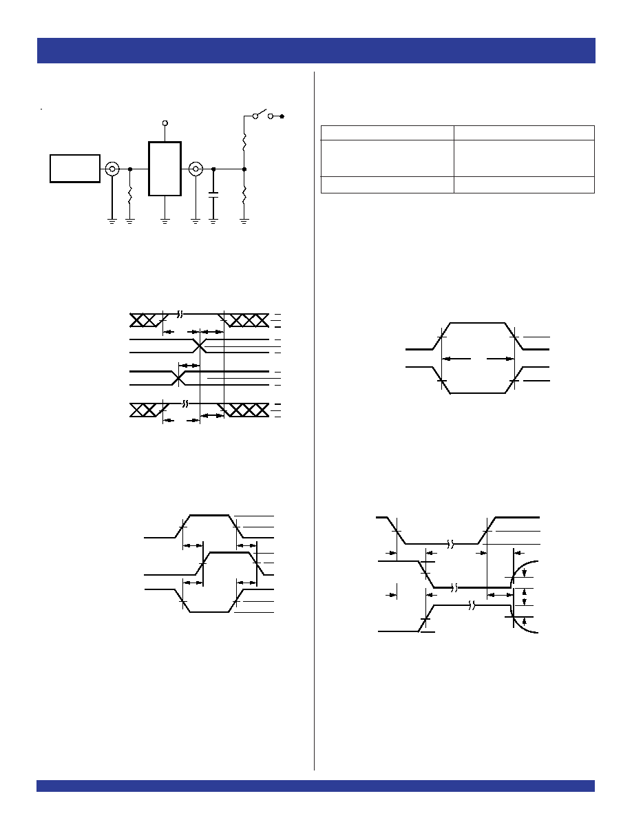
1. See test circuit and waveforms.
2. Minimum limits are guaranteed but not tested on Propagation Delays.
MILITARY AND INDUSTRIAL TEMPERATURE RANGES
IDT54/74FCT541T/AT/CT
FAST CMOS OCTAL BUFFER/LINE DRIVER
5
Pulse
Generator
R
T
D.U.T
.
V
CC
V
IN
C
L
V
OUT
50pF
500
500
7.0V
3V
1.5V
0V
3V
1.5V
0V
3V
1.5V
0V
3V
1.5V
0V
DATA
INPUT
TIMING
INPUT
ASYNCHRONOUS CONTROL
PRESET
CLEAR
ETC.
SYNCHRONOUS CONTROL
t
SU
t
H
t
REM
t
SU
t
H
HIGH-LOW-HIGH
PULSE
LOW-HIGH-LOW
PULSE
t
W
1.5V
1.5V
SAME PHASE
INPUT TRANSITION
3V
1.5V
0V
1.5V
V
OH
t
PLH
OUTPUT
OPPOSITE PHASE
INPUT TRANSITION
3V
1.5V
0V
t
PLH
t
PHL
t
PHL
V
OL
CONTROL
INPUT
3V
1.5V
0V
3.5V
0V
OUTPUT
NORMALLY
LOW
OUTPUT
NORMALLY
HIGH
SWITCH
CLOSED
SWITCH
OPEN
V
OL
0.3V
0.3V
t
PLZ
t
PZL
t
PZH
t
PHZ
3.5V
0V
1.5V
1.5V
ENABLE
DISABLE
V
OH
PRESET
CLEAR
CLOCK ENABLE
ETC.
Octal link
Octal link
Octal link
Octal link
Octal link
TEST CIRCUITS AND WAVEFORMS
Propagation Delay
Test Circuits for All Outputs
Enable and Disable Times
Set-Up, Hold, and Release Times
Pulse Width
NOTES:
1. Diagram shown for input Control Enable-LOW and input Control Disable-HIGH.
2. Pulse Generator for All Pulses: Rate
1.0MHz; t
F
2.5ns; t
R
2.5ns.
Test
Switch
Open Drain
Disable Low
Closed
Enable Low
All Other Tests
Open
SWITCH POSITION
DEFINITIONS:
C
L
= Load capacitance: includes jig and probe capacitance.
R
T
= Termination resistance: should be equal to Z
OUT
of the Pulse Generator.
MILITARY AND INDUSTRIAL TEMPERATURE RANGES
6
IDT54/74FCT541T/AT/CT
FAST CMOS OCTAL BUFFER/LINE DRIVER
ORDERING INFORMATION
IDT XX
Temp. Range
FCT
XXXX
Device Type
XX
Package
X
Process
Fast CMOS Octal Buffer/Line Driver
541T
541AT
541CT
SO
PY
Q
PG
Industrial Options
Small Outline IC
Shrink Small Outline Package
Quarter-size Small Outline Package
Thin Shrink Small Outline Package
D
L
Military Options
CERDIP
Leadless Chip Carrier
Blank
B
Industrial
MIL-STD-883, Class B
54
74
≠ 55∞C to +125∞C
≠ 40∞C to +85∞C
CORPORATE HEADQUARTERS
for SALES:
for Tech Support:
2975 Stender Way
800-345-7015 or 408-727-6116
logichelp@idt.com
Santa Clara, CA 95054
fax: 408-492-8674
(408) 654-6459
www.idt.com