Integrated Device Technology, Inc.
MILITARY AND COMMERCIAL TEMPERATURE RANGES
MAY 1992
©
1992 Integrated Device Technology, Inc.
7.17
DSC-4602/3
Æ
FAST CMOS
OCTAL LATCHED
TRANSCEIVER
FEATURES:
∑ IDT54/74FCT543 equivalent to FAST
TM
speed
∑ IDT54/74FCT543A 25% faster than FAST
∑ IDT54/74FCT543C 40% faster than FAST
∑ Equivalent to FAST output drive over full temperature
and voltage supply extremes
∑ I
OL
= 64mA (commercial), 48mA (military)
∑ Separate controls for data flow in each direction
∑ Back-to-back latches for storage
∑ CMOS power levels (1mW typ. static)
∑ Substantially lower input current levels than FAST
(5
µ
A max.)
∑ TTL input and output level compatible
∑ CMOS output level compatible
∑ Product available in Radiation Tolerant and Radiation
Enhanced versions
∑ Military product compliant to MIL-STD-883, Class B
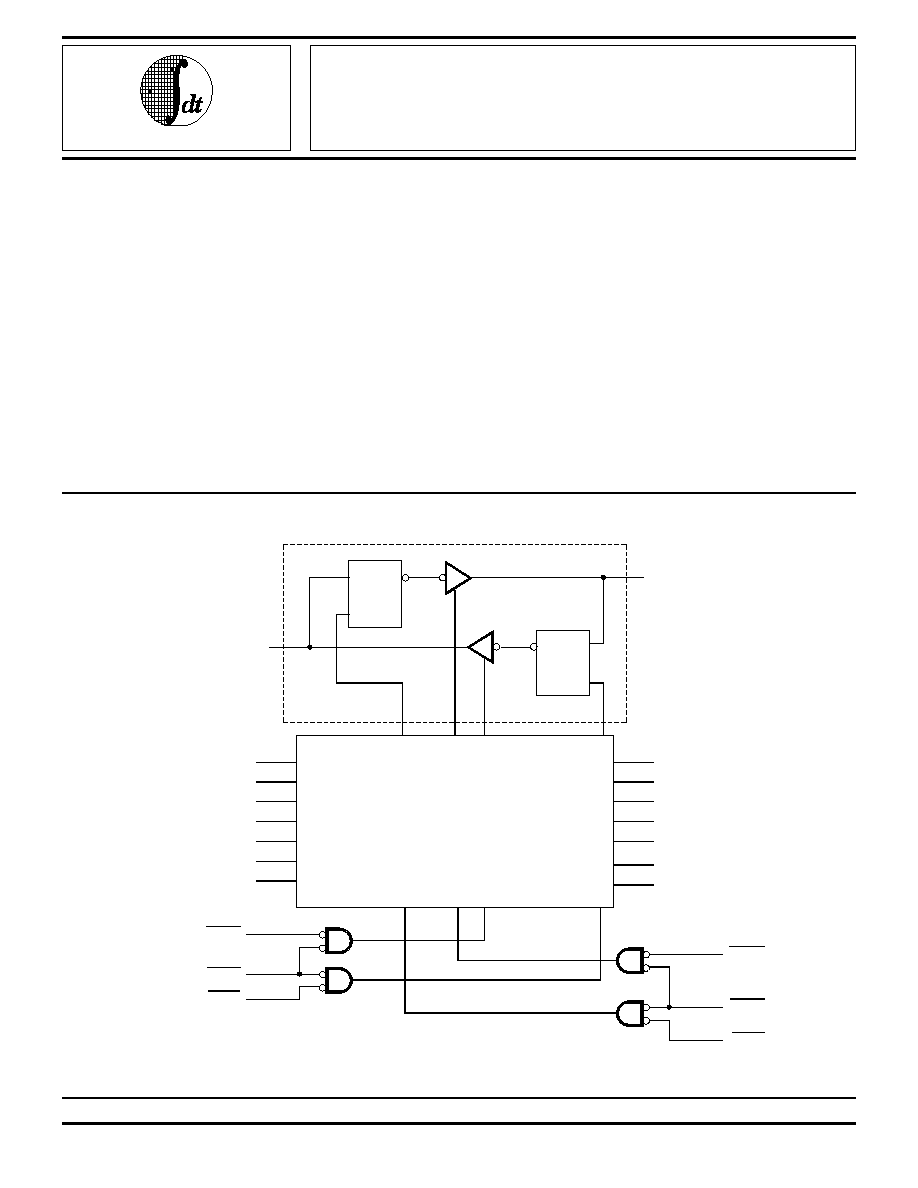
DESCRIPTION:
The IDT54/74FCT543/A/C is a non-inverting octal trans-
ceiver built using an advanced dual metal CMOS technology.
These devices contain two sets of eight D-type latches with
separate input and output controls for each set. For data flow
from A to B, for example, the A-to-B Enable (
CEAB
) input must
be LOW in order to enter data from A
0
≠A
7
or to take data from
B
0
≠B
7
, as indicated in the Function Table. With
CEAB
LOW,
a LOW signal on the A-to-B Latch Enable (
LEAB
) input makes
the A-to-B latches transparent; a subsequent LOW-to-HIGH
transition of the
LEAB
signal puts the A latches in the storage
mode and their outputs no longer change with the A inputs.
With
CEAB
and
OEAB
both LOW, the 3-state B output buffers
are active and reflect the data present at the output of the A
latches. Control of data from B to A is similar, but uses the
CEBA
,
LEBA
and
OEBA
inputs.
FUNCTIONAL BLOCK DIAGRAMS
A
1
2614 drw 01
Q
OEBA
A
2
A
3
A
4
A
5
A
6
A
7
B
1
B
2
B
3
B
4
B
5
B
6
B
7
CEBA
LEBA
OEAB
CEAB
LEAB
DETAIL A x 7
D
LE
Q
D
LE
DETAIL A
A
0
B
0
The IDT logo is a registered trademark of Integrated Device Technology, Inc.
FAST is a registered trademark of National Semiconductor Co.
IDT54/74FCT543
IDT54/74FCT543A
IDT54/74FCT543C
1
7.17
2
IDT54/74FCT543/A/C
FAST CMOS OCTAL LATCHED TRANSCEIVER
MILITARY AND COMMERCIAL TEMPERATURE RANGES
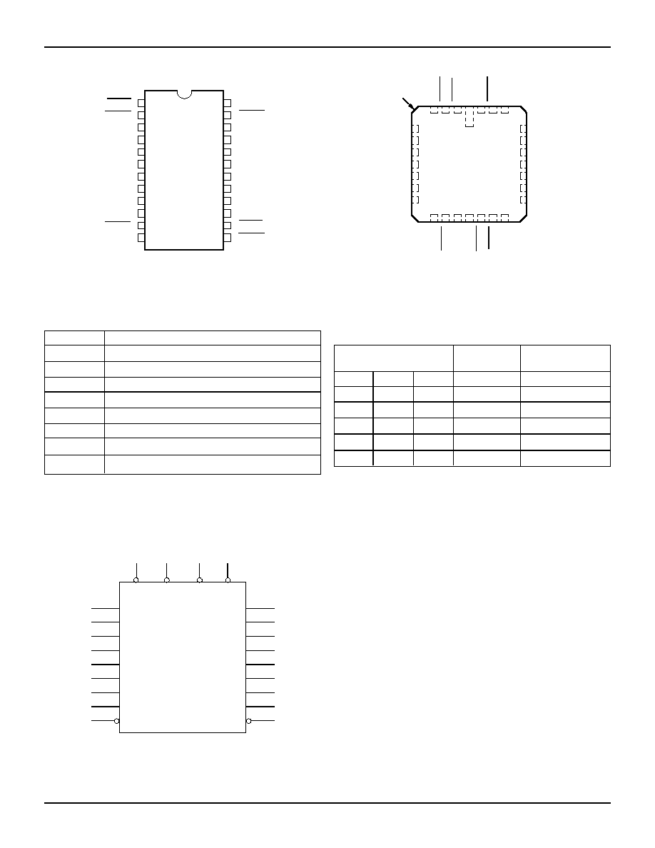
PIN CONFIGURATIONS
IDT54/74FCT861 10-BIT TRANSCEIVERS
PIN DESCRIPTION
Pin Names
Description
OEAB
A-to-B Output Enable Input (Active LOW)
OEBA
B-to-A Output Enable Input (Active LOW)
CEAB
A-to-B Enable Input (Active LOW)
CEBA
B-to-A Enable Input (Active LOW)
LEAB
A-to-B Latch Enable Input (Active LOW)
LEBA
B-to-A Latch Enable Input (Active LOW)
A
0
≠A
7
A-to-B Data Inputs or B-to-A 3-State Outputs
B
0
≠B
7
B-to-A Data Inputs or A-to-B 3-State Outputs
2614 tbl 02
FUNCTION TABLE
(1,2)
For A-to-B (Symmetric with B-to-A)
Latch
Output
Inputs
Status
Buffers
CEAB
CEAB
LEAB
LEAB
OEAB
OEAB
A-to-B
B
0
≠B
7
H
--
--
Storing
High Z
--
H
--
Storing
--
--
--
H
--
High Z
L
L
L
Transparent
Current A Inputs
L
H
L
Storing
Previous* A Inputs
LOGIC SYMBOL
A
1
2614 drw 03
A
2
A
3
A
4
A
5
A
6
A
7
OEBA
A
0
B
1
B
2
B
3
B
4
B
5
B
6
B
7
B
0
OEAB
LEAB CEAB CEBA LEBA
LCC
TOP VIEW
NOTES:
2614 tbl 01
1. * Before
LEAB
LOW-to-HIGH Transition
H = HIGH Voltage Level
L = LOW Voltage Level
-- = Don't Care or Irrelevant
2. A-to-B data flow shown; B-to-A flow control is the same, except using
CEBA
,
LEBA
and
OEBA
.
DIP/SOIC/CERPACK
TOP VIEW
2614 drw 02
5
6
7
8
9
10
11
L28-1
25
24
23
22
21
20
19
INDEX
A
1
A
2
A
3
A
4
A
5
A
6
NC
Vcc
GND
NC
NC
NC
B
1
B
2
B
3
B
4
B
5
B
6
A
0
LEBA
OEBA
B
0
CEBA
A
7
CEAB
B
7
LEAB
OEAB
12 13 14 15 16 17 18
4
3
2
1
28 27 26
5
6
7
8
9
10
11
12
GND
A
0
A
1
A
2
1
2
3
4
24
23
22
21
20
19
18
17
Vcc
16
15
14
13
P24-1,
D24-1,
SO24-2
&
E24-1
B
0
A
3
A
4
A
5
A
6
A
7
B
1
B
2
B
3
B
4
B
5
B
6
B
7
LEAB
OEAB
LEBA
OEBA
CEAB
CEBA
IDT54/74FCT543/A/C
FAST CMOS OCTAL LATCHED TRANSCEIVER
MILITARY AND COMMERCIAL TEMPERATURE RANGES
7.17
3
DC ELECTRICAL CHARACTERISTICS OVER OPERATING RANGE
Following Conditions Apply Unless Otherwise Specified: V
LC
= 0.2V, V
HC
= V
CC
≠ 0.2V
Commercial: T
A
= 0
∞
C to +70
∞
C, V
CC
= 5.0V
±
5%; Military: T
A
= ≠55
∞
C to +125
∞
C, V
CC
= 5.0V
±
10%
Symbol
Parameter
Test Conditions
(1)
Min.
Typ.
(2)
Max.
Unit
V
IH
Input HIGH Level
Guaranteed Logic HIGH Level
2.0
--
--
V
V
IL
Input LOW Level
Guaranteed Logic LOW Level
--
--
0.8
V
I
IH
Input HIGH Current
V
CC
= Max.
V
I
= V
CC
--
--
5
µ
A
(Except I/O pins)
V
I
= 2.7V
--
--
5
(4)
I
IL
Input LOW Current
V
I
= 0.5V
--
--
≠5
(4)
µ
A
(Except I/O pins)
V
I
= GND
--
--
≠5
I
IH
Input HIGH Current
V
CC
= Max.
V
I
= V
CC
--
--
15
µ
A
(I/O pins Only)
V
I
= 2.7V
--
--
15
(4)
I
IL
Input LOW Current
V
I
= 0.5V
--
--
≠15
(4)
µ
A
(I/O pins Only)
V
I
= GND
--
--
≠15
V
IK
Clamp Diode Voltage
V
CC
= Min., I
N
= ≠18mA
--
≠0.7
≠1.2
V
I
OS
Short Circuit Current
V
CC
= Max.
(3)
, V
O
= GND
≠60
≠120
--
mA
V
OH
Output HIGH Voltage
V
CC
= 3V, V
IN
= V
LC
or V
HC
, I
OH
= ≠32
µ
A
V
HC
V
CC
--
V
V
CC
= Min.
I
OH
= ≠300
µ
A
V
HC
(4)
V
CC
--
V
IN
= V
IH
or V
IL
I
OH
= ≠12mA MIL.
2.4
4.3
--
I
OH
= ≠15mA COM'L.
2.4
4.3
--
V
OL
Output LOW Voltage
V
CC
= 3V, V
IN
= V
LC
or V
HC
, I
OL
= 300
µ
A
--
GND
V
LC
V
V
CC
= Min.
I
OL
= 300
µ
A
--
GND
V
LC
(4)
V
IN
= V
IH
or V
IL
I
OL
= 48mA MIL.
(5)
--
0.3
0.55
I
OL
= 64mA COM'L.
(5)
--
0.3
0.55
NOTES:
2614 tbl 05
1. For conditions shown as Max. or Min., use appropriate value specified under Electrical Characteristics for the applicable device type.
2. Typical values are at V
CC
= 5.0V, +25
∞
C ambient and maximum loading.
3. Not more than one output should be shorted at one time. Duration of the short circuit test should not exceed one second.
4. This parameter is guaranteed but not tested.
5. These are maximum I
OL
values per output, for 8 outputs turned on simultaneously. Total maximum I
OL
(all outputs) is 512mA for commercial and 384mA
for military. Derate I
OL
for number of outputs exceeding 8 turned on simultaneously.
CAPACITANCE
(T
A
= +25
∞
C, f = 1.0MHz)
Symbol
Parameter
(1)
Conditions Typ.
Max.
Unit
C
IN
Input Capacitance
V
IN
= 0V
6
10
pF
C
I/O
I/O Capacitance
V
OUT
= 0V
8
12
pF
NOTE:
2614 tbl 04
1. This parameter is guaranteed by characterization data and not tested.
ABSOLUTE MAXIMUM RATINGS
(1)
Symbol
Rating
Commercial
Military
Unit
V
TERM
(2)
Terminal Voltage
≠0.5 to +7.0 ≠0.5 to +7.0
V
with Respect
to GND
V
TERM
(3)
Terminal Voltage
≠0.5 to V
CC
≠0.5 to V
CC
V
with Respect
to GND
T
A
Operating
0 to +70
≠55 to +125
∞
C
Temperature
T
BIAS
Temperature
≠55 to +125 ≠65 to +135
∞
C
Under Bias
T
STG
Storage
≠55 to +125 ≠65 to +150
∞
C
Temperature
P
T
Power Dissipation
0.5
0.5
W
I
OUT
DC Output Current
120
120
mA
NOTES:
2614 tbl 03
1. Stresses greater than those listed under ABSOLUTE MAXIMUM
RATINGS may cause permanent damage to the device. This is a stress
rating only and functional operation of the device at these or any other
conditions above those indicated in the operational sections of this
specification is not implied. Exposure to absolute maximum rating
conditions for extended periods may affect reliability. No terminal voltage
may exceed V
CC
by +0.5V unless otherwise noted.
2. Inputs and V
CC
terminals only.
3. Outputs and I/O terminals only.
7.17
4
IDT54/74FCT543/A/C
FAST CMOS OCTAL LATCHED TRANSCEIVER
MILITARY AND COMMERCIAL TEMPERATURE RANGES
POWER SUPPLY CHARACTERISTICS
V
LC
= 0.2V; V
HC
= V
CC
≠ 0.2V
Symbol
Parameter
Test Conditions
(1)
Min.
Typ.
(2)
Max.
Unit
I
CC
Quiescent Power
V
CC
= Max.
--
0.2
1.5
mA
Supply Current
V
IN
V
HC
; V
IN
V
LC
I
CC
Quiescent Power Supply
V
CC
= Max., V
IN
= 3.4V
(3)
--
0.5
2.0
mA
Current TTL Inputs HIGH
I
CCD
Dynamic Power Supply Current
(4)
V
CC
= Max., Outputs Open
V
IN
V
HC
--
0.15
0.25
mA/
CEAB
and
OEAB
= GND
V
IN
V
LC
MHz
CEBA
= V
CC
One Input Toggling
50% Duty Cycle
I
C
Total Power Supply Current
(6)
V
CC
= Max., Outputs Open
V
IN
V
HC
--
1.7
4.0
mA
f
CP
= 10MHz (
LEAB
)
V
IN
V
LC
50% Duty Cycle
(FCT)
CEAB
and
OEAB
= GND
CEBA
= V
CC
One Bit Toggling
V
IN
= 3.4V
--
2.2
6.0
at f
i
= 5MHz
V
IN
= GND
50% Duty Cycle
V
CC
= Max., Outputs Open
V
IN
V
HC
--
7.0
12.8
(5)
f
CP
= 10MHz (
LEAB
)
V
IN
V
LC
50% Duty Cycle
(FCT)
CEAB
and
OEAB
= GND
CEBA
= V
CC
Eight Bits Toggling
V
IN
= 3.4V
--
9.2
21.8
(5)
at f
i
= 5MHz
V
IN
= GND
50% Duty Cycle
NOTES:
2614 tbl 06
1. For conditions shown as Max. or Min., use appropriate value specified under Electrical Characteristics for the applicable device type.
2. Typical values are at V
CC
= 5.0V, +25
∞
C ambient.
3. Per TTL driven input (V
IN
= 3.4V); all other inputs at V
CC
or GND.
4. This parameter is not directly testable, but is derived for use in Total Power Supply calculations.
5. Values for these conditions are examples of the I
CC
formula. These limits are guaranteed but not tested.
6. I
C
= I
QUIESCENT
+I
INPUTS
+ I
DYNAMIC
I
C
= I
CC
+
I
CC
D
H
N
T
+ I
CCD
(f
CP
/2 + f
i
N
i
)
I
CC
= Quiescent Current
I
CC
= Power Supply Current for a TTL High Input (V
IN
= 3.4V)
D
H
= Duty Cycle for TTL Inputs High
N
T
= Number of TTL Inputs at D
H
I
CCD
= Dynamic Current Caused by an Input Transition Pair (HLH or LHL)
f
CP
= Clock Frequency for Register Devices (Zero for Non-Register Devices)
f
i
= Input Frequency
N
i
= Number of Inputs at f
i
All currents are in milliamps and all frequencies are in megahertz.

IDT54/74FCT543/A/C
FAST CMOS OCTAL LATCHED TRANSCEIVER
MILITARY AND COMMERCIAL TEMPERATURE RANGES
7.17
5
SWITCHING CHARACTERISTICS OVER OPERATING RANGE
IDT54/74FCT543
IDT54/74FCT543A
IDT54/74FCT543C
Com'l.
Mil.
Com'l.
Mil.
Com'l.
Mil.
Symbol
Parameter
Condition
(1)
Min.
(2)
Max
.
Min.
(2)
Max. Min.
(2)
Max. Min.
(2)
Max. Min.
(2)
Max. Min.
(2)
Max.
Unit
t
PLH
Propagation Delay
C
L
= 50pF
2.5
8.5
2.5
10.0
2.5
6.5
2.5
7.5
2.5
5.3
2.5
6.1
ns
t
PHL
Transparent Mode
R
L
= 500
A
n
to B
n
or B
n
to A
n
t
PLH
Propagation Delay
2.5
12.5
2.5
14.0
2.5
8.0
2.5
9.0
2.5
7.0
2.5
8.0
ns
t
PHL
LEBA
to A
n
,
LEAB
to B
n
t
PZH
Output Enable Time
2.0
12.0
2.0
14.0
2.0
9.0
2.0
10.0
2.0
8.0
2.0
9.0
ns
t
PZL
OEBA
or
OEAB
to A
n
or B
n
CEBA
or
CEAB
to A
n
or B
n
t
PHZ
Output Disable Time
2.0
9.0
2.0
13.0
2.0
7.5
2.0
8.5
2.0
6.5
2.0
7.5
ns
t
PLZ
OEBA
or
OEAB
to A
n
or B
n
CEBA
or
CEAB
to A
n
or B
n
t
SU
Set-up Time, HIGH or LOW
3.0
--
3.0
--
2.0
--
2.0
--
2.0
--
2.0
--
ns
A
n
or B
n
to
LEBA
or
LEAB
t
H
Hold Time, HIGH or LOW
2.0
--
2.0
--
2.0
--
2.0
--
2.0
--
2.0
--
ns
A
n
or B
n
to
LEBA
or
LEAB
t
W
LEBA
or
LEAB
Pulse Width
5.0
--
5.0
--
5.0
--
5.0
--
5.0
--
5.0
--
ns
LOW
NOTES:
2513 tbl 07
1. See test circuits and waveforms.
2. Minimum limits are guaranteed but not tested on Propagation Delays.