Äîêóìåíòàöèÿ è îïèñàíèÿ www.docs.chipfind.ru
MILITARY AND INDUSTRIAL TEMPERATURE RANGES
IDT54/74FCT573T/AT/CT
FAST CMOS OCTAL TRANSPARENT LATCH
1
JUNE 2002
MILITARY AND INDUSTRIAL TEMPERATURE RANGES
The IDT logo is a registered trademark of Integrated Device Technology, Inc.
© 2002 Integrated Device Technology, Inc.
DSC-5948/3
FEATURES:
· Std., A, and C grades
· Low input and output leakage
1µA (max.)
· CMOS power levels
· True TTL input and output compatibility:
V
OH
= 3.3V (typ.)
V
OL
= 0.3V (typ.)
· High Drive outputs (-15mA I
OH
, 48mA I
OL
)
· Meets or exceeds JEDEC standard 18 specifications
· Military product compliant to MIL-STD-883, Class B and DESC
listed (dual marked)
· Power off disable outputs permit "live insertion"
· Available in the following packages:
Industrial: SOIC, SSOP, QSOP, TSSOP
Military: CERDIP, LCC
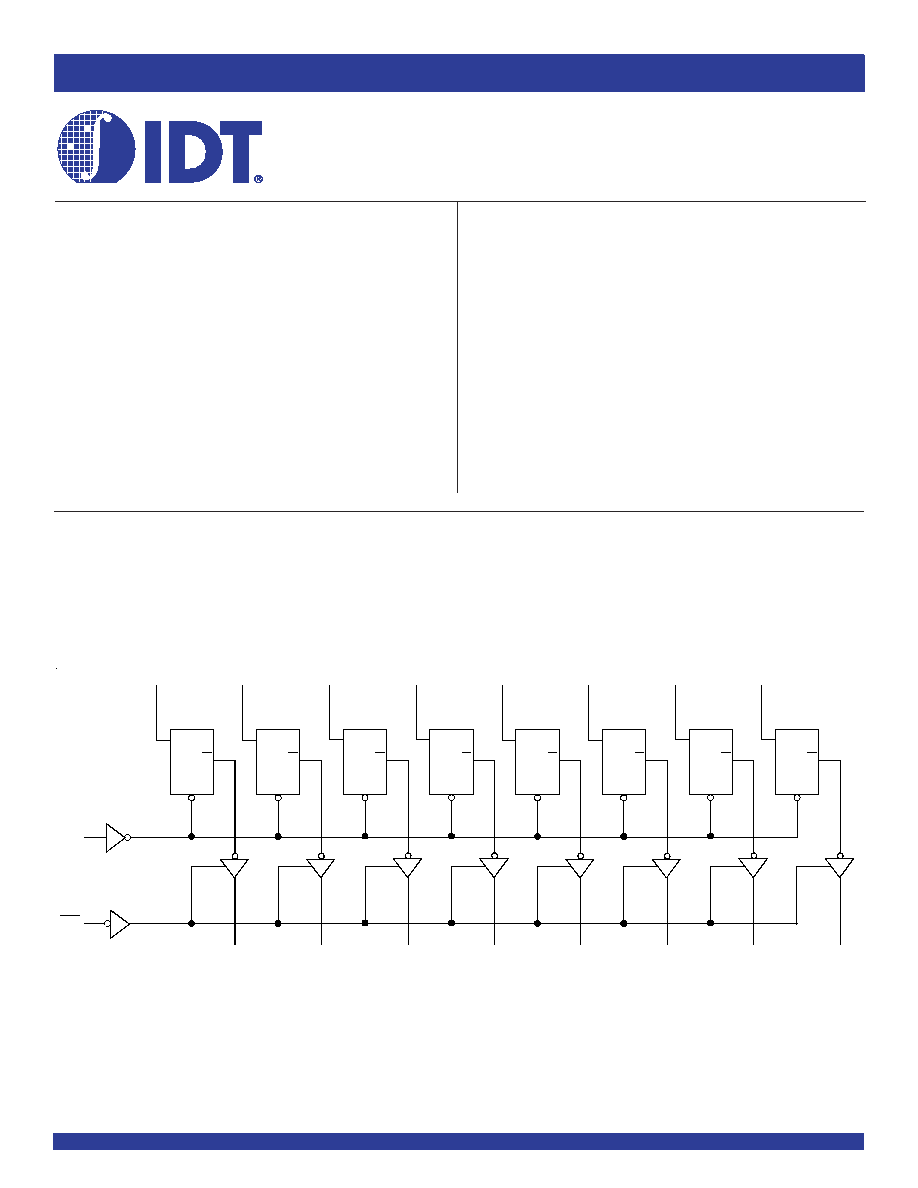
FUNCTIONAL BLOCK DIAGRAM
IDT54/74FCT573T/AT/CT
FAST CMOS OCTAL
TRANSPARENT LATCH
DESCRIPTION:
The FCT573Tis an octal transparent latch built using an advanced dual
metal CMOS technology. These octal latches have 3-state outputs and are
intended for bus oriented applications. The flip-flops appear transparent to
the data when Latch Enable (LE) is high. When LE is low, the data that meets
the set-up time is latched. Data appears on the bus when the Output Enable
(OE) is low. When OE is high, the bus output is in the high-impedance state.
LE
D
G
O
O
0
D
0
D
G
O
O
1
D
1
D
G
O
O
2
D
2
D
G
O
O
3
D
3
D
G
O
O
4
D
4
D
G
O
O
5
D
5
D
G
O
O
6
D
6
D
G
O
O
7
D
7
OE
MILITARY AND INDUSTRIAL TEMPERATURE RANGES
2
IDT54/74FCT573T/AT/CT
FAST CMOS OCTAL TRANSPARENT LATCH
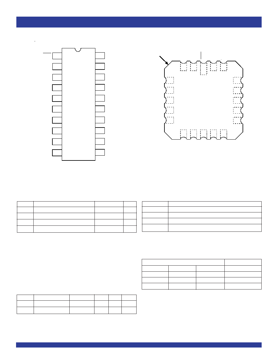
PIN CONFIGURATION
Symbol
Description
Max
Unit
V
TERM
(2)
Terminal Voltage with Respect to GND
0.5 to +7
V
V
TERM
(3)
Terminal Voltage with Respect to GND
0.5 to V
CC
+0.5
V
T
STG
Storage Temperature
65 to +150
°C
I
OUT
DC Output Current
60 to +120
mA
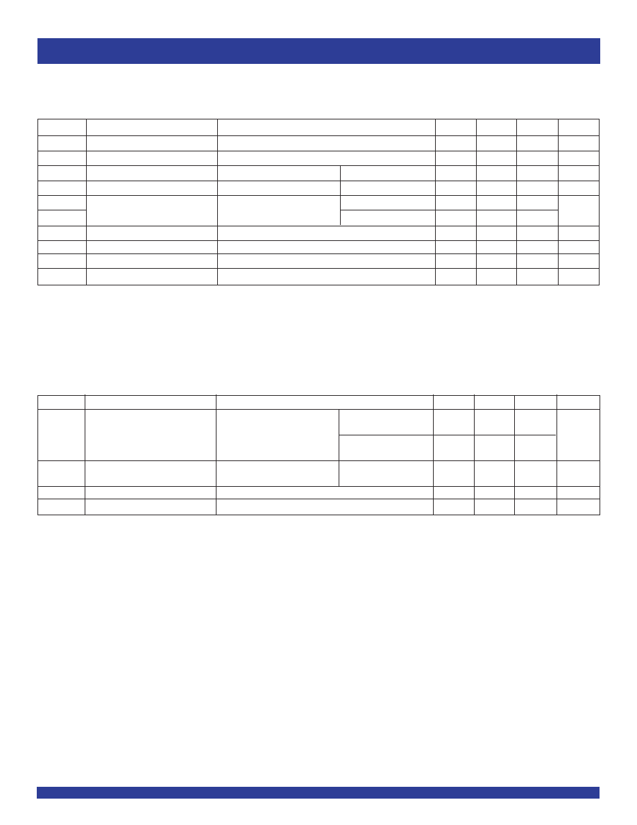
ABSOLUTE MAXIMUM RATINGS
(1)
NOTES:
1. Stresses greater than those listed under ABSOLUTE MAXIMUM RATINGS may cause
permanent damage to the device. This is a stress rating only and functional operation
of the device at these or any other conditions above those indicated in the operational
sections of this specification is not implied. Exposure to absolute maximum rating
conditions for extended periods may affect reliability. No terminal voltage may exceed
Vcc by +0.5V unless otherwise noted.
2. Inputs and Vcc terminals only.
3. Output and I/O terminals only.
Symbol
Parameter
(1)
Conditions
Typ.
Max.
Unit
C
IN
Input Capacitance
V
IN
= 0V
6
10
pF
C
OUT
Output Capacitance
V
OUT
= 0V
8
12
pF
CAPACITANCE
(T
A
= +25°C, F = 1.0MHz)
NOTE:
1. This parameter is measured at characterization but not tested.
PIN DESCRIPTION
Pin Names
Description
Dx
Data Inputs
LE
Latch Enable Input (Active HIGH)
OE
Output Enable Input (Active LOW)
Ox
3-State Outputs
CERDIP/ SOIC/ SSOP/ QSOP/ TSSOP
TOP VIEW
2
3
1
16
15
14
11
19
18
20
17
13
12
5
6
7
4
8
9
10
D
2
D
0
D
1
V
CC
D
3
D
6
D
4
D
5
D
7
GND
O
0
O
3
O
1
O
2
O
4
O
7
O
5
O
6
LE
OE
1
2
3
4
5
7
9
6
8
10
11
12
13
14
15
16
17
18
19
20
O
3
O
1
O
2
O
4
O
5
D
1
D
0
D
7
G
N
D
L
E
O
7
O
6
O
E
V
C
C
O
0
INDEX
D
6
D
2
D
5
D
3
D
4
LCC
TOP VIEW
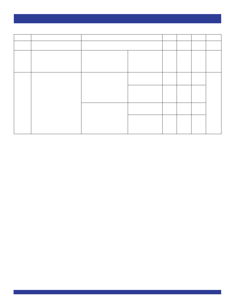
NOTE:
1. H = HIGH Voltage Level
X = Don't Care
L = LOW Voltage Level
Z = High Impedance
FUNCTION TABLE
(1)
Inputs
Outputs
Dx
LE
OE
Ox
H
H
L
H
L
H
L
L
X
X
H
Z
MILITARY AND INDUSTRIAL TEMPERATURE RANGES
IDT54/74FCT573T/AT/CT
FAST CMOS OCTAL TRANSPARENT LATCH
3
NOTES:
1. For conditions shown as Min. or Max., use appropriate value specified under Electrical Characteristics for the applicable device type.
2. Typical values are at V
CC
= 5.0V, +25°C ambient.
3. Not more than one output should be tested at one time. Duration of the test should not exceed one second.
4. The test limit for this parameter is ±5µA at T
A
= 55°C.
5. This parameter is guaranteed but not tested.
Symbol
Parameter
Test Conditions
(1)
Min.
Typ.
(2)
Max.
Unit
V
OH
Output HIGH Voltage
V
CC
= Min
I
OH
= 6mA MIL
2.4
3.3
--
V
IN
= V
IH
or V
IL
I
OH
= 8mA IND
V
I
OH
= 12mA MIL
2
3
--
I
OH
= 15mA IND
V
OL
Output LOW Voltage
V
CC
= Min
I
OL
= 32mA MIL
--
0.3
0.5
V
V
IN
= V
IH
or V
IL
I
OL
= 48mA IND
I
OS
Short Circuit Current
V
CC
= Max., V
O
= GND
(3)
60
120
225
mA
I
OFF
Input/Output Power Off Leakage
(5)
V
CC
= 0V, V
IN
or V
O
4.5V
--
--
±1
µA
OUTPUT DRIVE CHARACTERISTICS
Symbol
Parameter
Test Conditions
(1)
Min.
Typ.
(2)
Max.
Unit
V
IH
Input HIGH Level
Guaranteed Logic HIGH Level
2
--
--
V
V
IL
Input LOW Level
Guaranteed Logic LOW Level
--
--
0.8
V
I
IH
Input HIGH Current
(4)
V
CC
= Max.
V
I
= 2.7V
--
--
±1
µA
I
IL
Input LOW Current
(4)
V
CC
= Max.
V
I
= 0.5V
--
--
±1
µA
I
OZH
High Impedance Output Current
V
CC
= Max
V
O
= 2.7V
--
--
±1
µA
I
OZL
(3-State output pins)
(4)
V
O
= 0.5V
--
--
±1
I
I
Input HIGH Current
(4)
V
CC
= Max., V
I
= V
CC
(Max.)
--
--
±1
µA
V
IK
Clamp Diode Voltage
V
CC
= Min, I
IN
= -18mA
--
0.7
1.2
V
V
H
Input Hysteresis
--
--
200
--
mV
I
CC
Quiescent Power Supply Current
V
CC
= Max., V
IN
= GND or V
CC
--
0.01
1
mA
DC ELECTRICAL CHARACTERISTICS OVER OPERATING RANGE
Following Conditions Apply Unless Otherwise Specified:
Industrial: T
A
= 40°C to +85°C, V
CC
= 5.0V ±5%; Military: T
A
= 55°C to +125°C, V
CC
= 5.0V ±10%
MILITARY AND INDUSTRIAL TEMPERATURE RANGES
4
IDT54/74FCT573T/AT/CT
FAST CMOS OCTAL TRANSPARENT LATCH
Symbol
Parameter
Test Conditions
(1)
Min.
Typ.
(2)
Max.
Unit
I
CC
Quiescent Power Supply Current
V
CC
= Max.
--
0.5
2
mA
TTL Inputs HIGH
V
IN
= 3.4V
(3)
I
CCD
Dynamic Power Supply
V
CC
= Max.
V
IN
= V
CC
--
0.15
0.25
mA/
Current
(4)
Outputs Open
V
IN
= GND
MHz
OE = GND
One Input Toggling
50% Duty Cycle
I
C
Total Power Supply Current
(6)
V
CC
= Max.
V
IN
= V
CC
--
1.5
3.5
mA
Outputs Open
V
IN
= GND
fi = 10MHz
50% Duty Cycle
V
IN
= 3.4V
--
1.8
4.5
OE = GND
V
IN
= GND
LE = V
CC
One Bit Toggling
V
CC
= Max.
V
IN
= V
CC
--
3
6
(5)
mA
Outputs Open
V
IN
= GND
fi = 2.5MHz
50% Duty Cycle
V
IN
= 3.4V
--
5
14
(5)
OE = GND
V
IN
= GND
LE = V
CC
Eight Bits Toggling
NOTES:
1. For conditions shown as Min. or Max., use appropriate value specified under Electrical Characteristics for the applicable device type.
2. Typical values are at V
CC
= 5.0V, +25°C ambient.
3. Per TTL driven input; (V
IN
= 3.4V). All other inputs at V
CC
or GND.
4. This parameter is not directly testable, but is derived for use in Total Power Supply Calculations.
5. Values for these conditions are examples of
I
CC
formula. These limits are guaranteed but not tested.
6. I
C
= I
QUIESCENT
+ I
INPUTS
+ I
DYNAMIC
I
C
= I
CC
+
I
CC
D
H
N
T
+ I
CCD
(f
CP
/2+ f
i
N
i
)
I
CC
= Quiescent Current
I
CC
= Power Supply Current for a TTL High Input (V
IN
= 3.4V)
D
H
= Duty Cycle for TTL Inputs High
N
T
= Number of TTL Inputs at D
H
I
CCD
= Dynamic Current caused by an Input Transition Pair (HLH or LHL)
f
CP
= Clock Frequency for Register Devices (Zero for Non-Register Devices)
f
i
= Output Frequency
N
i
= Number of Outputs at f
i
All currents are in milliamps and all frequencies are in megahertz.
POWER SUPPLY CHARACTERISTICS
MILITARY AND INDUSTRIAL TEMPERATURE RANGES
IDT54/74FCT573T/AT/CT
FAST CMOS OCTAL TRANSPARENT LATCH
5
NOTES:
1. See test circuit and waveforms.
2. Minimum limits are guaranteed but not tested on Propagation Delays.
3. This limit is guaranteed but not tested.
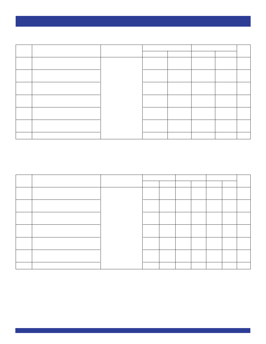
SWITCHING CHARACTERISTICS OVER OPERATING RANGE - MILITARY
54FCT573T
54FCT573AT
54FCT573CT
Symbol Parameter
Condition
(1)
Min
.
(2)
Max.
Min
.
(2)
Max.
Min
.
(2)
Max.
Unit
t
PLH
Propagation Delay
C
L
= 50pF
1.5
8.5
1.5
5.6
1.5
5.1
ns
t
PHL
Dx to Ox
R
L
= 500
t
PLH
Propagation Delay
2
15
2
9.8
2
8
ns
t
PHL
LE to Ox
t
PZH
Output Enable Time
1.5
13.5
1.5
7.5
1.5
6.3
ns
t
PZL
t
PHZ
Output Disable Time
1.5
10
1.5
6.5
1.5
5.9
ns
t
PLZ
t
SU
Set-up Time, HIGH or LOW
2
--
2
--
2
--
ns
Dx to LE
t
H
Hold Time, HIGH or LOW
1.5
--
1.5
--
1.5
--
ns
Dx to LE
t
W
LE Pulse Width HIGH
(3)
6
--
6
--
6
--
ns
SWITCHING CHARACTERISTICS OVER OPERATING RANGE - INDUSTRIAL
74FCT573AT
74FCT573CT
Symbol Parameter
Condition
(1)
Min
.
(2)
Max.
Min
.
(2)
Max.
Unit
t
PLH
Propagation Delay
C
L
= 50pF
1.5
5.2
1.5
4.2
ns
t
PHL
Dx to Ox
R
L
= 500
t
PLH
Propagation Delay
2
8.5
2
5.5
ns
t
PHL
LE to Ox
t
PZH
Output Enable Time
1.5
6.5
1.5
5.5
ns
t
PZL
t
PHZ
Output Disable Time
1.5
5.5
1.5
5
ns
t
PLZ
t
SU
Set-up Time, HIGH or LOW
2
--
2
--
ns
Dx to LE
t
H
Hold Time, HIGH or LOW
1.5
--
1.5
--
ns
Dx to LE
t
W
LE Pulse Width HIGH
(3)
5
--
5
--
ns