IDT54/74FCT623T/AT/CT
FAST CMOS OCTAL BUS TRANSCEIVERS (3-STATE)
6.19
1
Integrated Device Technology, Inc.
FAST CMOS OCTAL
BUS TRANSCEIVERS
(3-STATE)
IDT54/74FCT623T/AT/CT
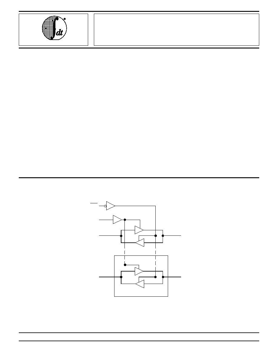
DESCRIPTION
The FCT623T/AT/CT is a non-inverting octal transceiver
with 3-state bus-driving outputs in both the send and receive
directions. The B bus outputs are capable of sinking 64mA and
sourcing up to 15mA, providing very good capacitive drive
characteristics.
These octal bus transceivers are designed for asynchro-
nous two-way communication between data buses. The control
function implementation allows for maximum flexibility in
timing.
One important feature of the FCT623T/AT/CT is the Power
Down Disable capability. When the GAB and
G
BA inputs are
conditioned to put the device in high-Z state, the I/O ports will
maintain high impedance during power supply ramps and
when V
CC
= 0V. This is a desirable feature in back-plane
applications where it may be necessary to perform "live"
insertion and removal of cards for on-line maintenance. It is
also a benefit in systems with multiple redundancy where one
or more redundant cards may be powered-off.
FUNCTIONAL BLOCK DIAGRAM
The IDT logo is a registered trademark of Integrated Device Technology, Inc.
1
MILITARY AND COMMERCIAL TEMPERATURE RANGES
NOVEMBER 1995
©
1996 Integrated Device Technology, Inc.
6.19
DSC-2563/5
FEATURES:
∑ Std., A and C speed grades
∑ Low input and output leakage
1
µ
A (max.)
∑ CMOS power levels
∑ True TTL input and output compatibility
≠ V
OH
= 3.3V (typ.)
≠ V
OL
= 0.3V (typ.)
∑ High drive outputs (-15mA I
OH
, 64mA I
OL
)
∑ Power off disable outputs permit "live insertion"
∑ Meets or exceeds JEDEC standard 18 specifications
∑ Product available in Radiation Tolerant and Radiation
Enhanced versions
∑ Military product compliant to MIL-STD-883, Class B
and DESC listed (dual marked)
∑ Available in DIP, SOIC, CERPACK and LCC packages
GAB
A1
B1
A2 - A8
B2 - B8
7 other transceivers
GBA
2563 drw 01
MILITARY AND COMMERCIAL TEMPERATURE RANGES
IDT54/74FCT623T/AT/CT
FAST CMOS OCTAL BUS TRANSCEIVERS (3-STATE)
6.19
2
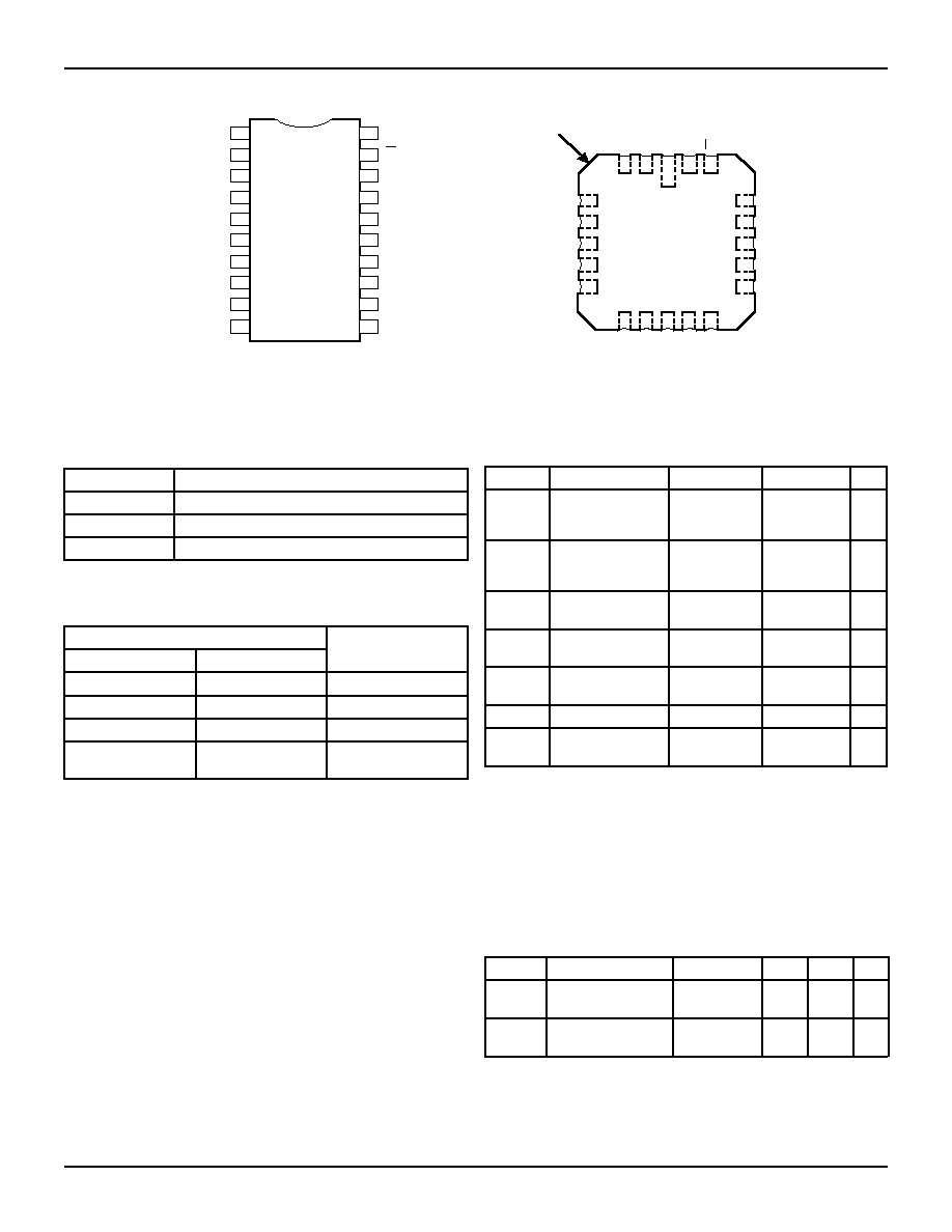
PIN CONFIGURATIONS
2563 drw 02
2563 drw 03
DEFINITION OF FUNCTIONAL TERMS
2563 tbl 01
ABSOLUTE MAXIMUM RATINGS
(1)
FUNCTION TABLE
(1)
GAB
A
1
A
2
A
3
A
4
A
5
A
6
A
7
A
8
GND
GBA
B
1
B
2
B
3
B
4
B
6
B
5
B
7
V
CC
1
2
3
4
5
6
7
8
9
10
11
12
13
14
15
16
17
18
19
20
DIP/SOIC/CERPACK
TOP VIEW
P20-1
D20-1
SO20-2
&
E20-1
INDEX
A
3
A
4
A
5
A
6
A
7
B
1
B
2
B
3
B
4
B
5
A
1
A
2
GAB
V
CC
GBA
A
8
GND
B
8
B
7
B
6
LCC
TOP VIEW
3
2
20 19
1
4
5
6
7
8
18
17
16
15
14
9 10 11 12 13
L20-2
B
8
Symbol
Rating
Commercial
Military
Unit
V
TERM(2)
Terminal Voltage
with Respect to
GND
≠0.5 to +7.0
≠0.5 to +7.0
V
V
TERM(3)
Terminal Voltage
with Respect to
GND
≠0.5 to
V
CC
+0.5
≠0.5 to
V
CC
+0.5
V
T
A
Operating
Temperature
0 to +70
≠55 to +125
∞
C
T
BIAS
Temperature
Under Bias
≠55 to +125
≠65 to +135
∞
C
T
STG
Storage
Temperature
≠55 to +125
≠65 to +150
∞
C
P
T
Power Dissipation
0.5
0.5
W
I
OUT
DC Output
Current
≠60 to +120 ≠60 to +120 mA
NOTES:
2563 tbl 02
1. H = HIGH Voltage Level
2. L = LOW Volage Level
3. Z = High-Impedance (OFF) state
CAPACITANCE (
T
A
= +25
∞
C, f = 1.0MHz)
Symbol
Parameter
(1)
Conditions
Typ.
Max. Unit
C
IN
Input
Capacitance
V
IN
= 0V
6
10
pF
C
OUT
Output
Capacitance
V
OUT
= 0V
8
12
pF
2563 lnk 03
NOTES:
1. Stresses greater than those listed under ABSOLUTE MAXIMUM RAT-
INGS may cause permanent damage to the device. This is a stress rating
only and functional operation of the device at these or any other conditions
above those indicated in the operational sections of this specification is
not implied. Exposure to absolute maximum rating conditions for
extended periods may affect reliability. No terminal voltage may exceed
V
CC
by +0.5V unless otherwise noted.
2. Input and V
CC
terminals only.
3. Outputs and I/O terminals only.
2563 lnk 04
NOTE:
1. This parameter is measured at characterization but not tested.
Pin Names
Description
G
BA, GAB
Enable Inputs
A
1
- A
8
A Bus Inputs or 3-State Outputs
B
1
- B
8
B Bus Inputs or 3-State Outputs
Enable Inputs
G
G
BA
GAB
Outputs
L
L
B data to A bus
H
H
A data to B bus
H
L
Z
L
H
B data to A bus
A data to B bus
IDT54/74FCT623T/AT/CT
FAST CMOS OCTAL BUS TRANSCEIVERS (3-STATE)
6.19
3
DC ELECTRICAL CHARACTERISTICS OVER OPERATING RANGE
Following Conditions Apply Unless Otherwise Specified:
Commercial: T
A
= 0
∞
C to +70
∞
C, V
CC
= 5.0V
±
5%; Military: T
A
= ≠55
∞
C to +125
∞
C, V
CC
= 5.0V
±
10%
NOTES:
2563 tbl 05
1. For conditions shown as Max. or Min., use appropriate value specified under Electrical Characteristics for the applicable device type.
2. Typical values are at V
CC
= 5.0V, +25
∞
C ambient.
3. Not more than one output should be shorted at one time. Duration of the short circuit test should not exceed one second.
4. These are maximum I
OL
values per output, for 8 outputs turned on simultaneously. Total maximum I
OL
(all outputs) is 512mA for commercial and 384mA
for military. Derate I
OL
for number of outputs exceeding 8 turned on simultaneously.
5. The test limit for this parameter is
±
5
µ
A at T
A
= ≠55
∞
C.
6. This parameter is guaranteed but not tested.
Symbol
Parameter
Test Conditions
(1)
Min.
Typ.
(2)
Max.
Unit
V
IH
Input HIGH Level
Guaranteed Logic HIGH Level
2.0
--
--
V
V
IL
Input LOW Level
Guaranteed Logic LOW Level
--
--
0.8
V
I
I H
Input HIGH Current
(5)
V
CC
= Max., V
I
= 2.7V
--
--
±
1
µ
A
I
I L
Input LOW Current
(5)
V
CC
= Max., V
I
= 0.5V
--
--
±
1
µ
A
I
I
Input HIGH Current
(5)
V
CC
= Max., V
I
= V
CC
(Max.)
--
--
±
1
µ
A
V
IK
Clamp Diode Voltage
V
CC
= Min., I
N
= ≠18mA
--
≠0.7
≠1.2
V
I
OS
Short Circuit Current
V
CC
= Max.
(3)
, V
O
= GND
≠60
≠120
≠225
mA
V
OH
Output HIGH Voltage
(A and B Bus)
V
CC
= Min.
V
IN
= V
IH
or V
IL
I
OH
= ≠6mA MIL.
I
OH
= ≠8mA COM'L.
2.4
3.3
--
V
I
OH
= ≠12mA MIL.
I
OH
= ≠15mA COM'L.
2.0
3.0
--
V
V
OL
Output LOW Voltage (A Bus)
V
CC
= Min.
V
IN
= V
IH
or V
IL
I
OL
= 32mA MIL.
(4)
I
OL
= 48mA COM'L.
--
0.3
0.5
V
V
OL
Output LOW Voltage (B Bus)
V
CC
= Min.
V
IN
= V
IH
or V
IL
I
OL
= 48mA MIL.
(4)
I
OL
= 64mA COM'L.
--
0.3
0.55
V
I
OFF
Input/Output Power Off Leakage
(6)
V
CC
= 0V, V
IN
or V
O
4.5V
--
--
±
1
µ
A
V
H
Input Hysteresis
--
--
200
--
mV
I
CC
Quiescent Power Supply Current
V
CC
= Max., V
IN
=
GND or V
CC
--
0.01
1
µ
A

MILITARY AND COMMERCIAL TEMPERATURE RANGES
IDT54/74FCT623T/AT/CT
FAST CMOS OCTAL BUS TRANSCEIVERS (3-STATE)
6.19
4
POWER SUPPLY CHARACTERISTICS
NOTES:
1. For conditions shown as Max. or Min., use appropriate value specified under Electrical Characteristics for the applicable device type.
2. Typical values are at V
CC
= 5.0V, +25
∞
C ambient.
3. Per TTL driven input (V
IN
= 3.4V). All other inputs at V
CC
or GND.
4. This parameter is not directly testable, but is derived for use in Total Power Supply Calculations.
5. Values for these conditions are examples of the I
CC
formula. These limits are guaranteed but not tested.
6. I
C
= I
QUIESCENT
+ I
INPUTS
+ I
DYNAMIC
I
C
= I
CC
+
I
CC
D
H
N
T
+ I
CCD
(f
CP/
2 + f
i
N
i
)
I
CC
= Quiescent Current
I
CC
= Power Supply Current for a TTL High Input (V
IN
= 3.4V)
D
H
= Duty Cycle for TTL Inputs High
N
T
= Number of TTL Inputs at D
H
I
CCD
= Dynamic Current Caused by an Input Transition Pair (HLH or LHL)
f
CP
= Clock Frequency for Register Devices (Zero for Non-Register Devices)
f
i
= Input Frequency
N
i
= Number of Inputs at f
i
All currents are in milliamps and all frequencies are in megahertz.
2563 tbl 07
Symbol
Parameter
Test Conditions
(1)
Min.
Typ.
(2)
Max.
Unit
I
CC
Quiescent Power Supply Current
TTL Inputs HIGH
V
CC
= Max.
V
IN
= 3.4V
(3)
--
0.5
2.0
mA
I
CCD
Dynamic Power Supply
Current
(4)
V
CC
= Max.
Outputs Open
G
BA = GAB = GND
One Input Toggling
50% Duty Cycle
V
IN
= V
CC
V
IN
= GND
--
0.15
0.25
mA/
MHz
I
C
Total Power Supply Current
(6)
V
CC
= Max.
Outputs Open
fi = 10MHz
V
IN
= V
CC
V
IN
= GND
--
1.5
3.5
mA
50% Duty Cycle
G
BA = GAB = GND
One Bit Toggling
V
IN
= 3.4V
V
IN
= GND
--
1.8
4.5
V
CC
= Max.
Outputs Open
fi = 2.5MHz
V
IN
= V
CC
V
IN
= GND
--
3.0
6.0
(5)
50% Duty Cycle
G
BA = GAB = GND
Eight Bits Toggling
V
IN
= 3.4V
V
IN
= GND
--
5.0
14.0
(5)
SWITCHING CHARACTERISTICS OVER OPERATING RANGE
NOTES:
2563 tbl 07
1. See test circuit and waveforms.
2. Minimum limits are guaranteed but not tested on Propagation Delays
54/74FCT623T
54/74FCT623AT
54/74FCT623CT
Com'l.
Mil.
Com'l.
Mil.
Com'l.
Mil.
Symbol
Parameter
Condition
(1)
Min.
(2)
Max. Min.
(2)
Max. Min.
(2)
Max. Min.
(2)
Max. Min.
(2)
Max. Min.
(2)
Max. Unit
t
PLH
t
PHL
Propagation Delay
An to Bn
C
L
= 50pF
R
L
= 500
1.5
7.5
1.5
9.0
1.5
5.5
1.5
6.3
1.5
4.8
1.5
5.4
ns
t
PLH
t
PHL
Propagation Delay
Bn to An
1.5
7.5
1.5
9.5
1.5
5.5
1.5
6.3
1.5
4.8
1.5
5.4
ns
t
PZH
t
PZL
Output Enable Time
G
BA to An
1.5
9.0
1.5
10.0
1.5
7.0
1.5
8.0
1.5
6.1
1.5
6.9
ns
t
PHZ
t
PLZ
Output Disable Time
G
BA to An
1.5
8.0
1.5
9.0
1.5
6.5
1.5
7.4
1.5
5.6
1.5
6.4
ns
t
PZH
t
PZL
Output Enable Time
GAB to Bn
1.5
9.0
1.5
10.5
1.5
7.0
1.5
8.0
1.5
6.1
1.5
6.9
ns
t
PHZ
t
PLZ
Output Disable Time
GAB to Bn
1.5
8.0
1.5
9.0
1.5
6.5
1.5
7.4
1.5
5.6
1.5
6.4
ns
IDT54/74FCT623T/AT/CT
FAST CMOS OCTAL BUS TRANSCEIVERS (3-STATE)
6.19
5
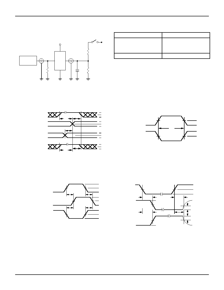
TEST CIRCUITS AND WAVEFORMS
TEST CIRCUITS FOR ALL OUTPUTS
ENABLE AND DISABLE TIMES
PROPAGATION DELAY
SET-UP, HOLD AND RELEASE TIMES
PULSE WIDTH
SWITCH POSITION
Pulse
Generator
R
T
D.U.T.
V
CC
V
IN
C
L
V
OUT
50pF
500
500
7.0V
3V
1.5V
0V
3V
1.5V
0V
3V
1.5V
0V
3V
1.5V
0V
DATA
INPUT
TIMING
INPUT
ASYNCHRONOUS CONTROL
PRESET
CLEAR
ETC.
SYNCHRONOUS CONTROL
t
SU
t
H
t
REM
t
SU
t
H
HIGH-LOW-HIGH
PULSE
LOW-HIGH-LOW
PULSE
t
W
1.5V
1.5V
SAME PHASE
INPUT TRANSITION
3V
1.5V
0V
1.5V
V
OH
t
PLH
OUTPUT
OPPOSITE PHASE
INPUT TRANSITION
3V
1.5V
0V
t
PLH
t
PHL
t
PHL
V
OL
CONTROL
INPUT
3V
1.5V
0V
3.5V
0V
OUTPUT
NORMALLY
LOW
OUTPUT
NORMALLY
HIGH
SWITCH
CLOSED
SWITCH
OPEN
V
OL
0.3V
0.3V
t
PLZ
t
PZL
t
PZH
t
PHZ
3.5V
0V
1.5V
1.5V
ENABLE
DISABLE
V
OH
PRESET
CLEAR
CLOCK ENABLE
ETC.
Test
Switch
Disable Low
Enable Low
Closed
All Other Tests
Open
Open Drain
DEFINITIONS:
C
L
=
Load capacitance: includes jig and probe capacitance.
R
T
=
Termination resistance: should be equal to Z
OUT
of the Pulse
Generator.
2563 lnk 09
2563 drw 05
2563 drw 06
2563 drw 07
2563 drw 08
2563 drw 09
NOTES:
1. Diagram shown for input Control Enable-LOW and input Control Disable-
HIGH
2. Pulse Generator for All Pulses: Rate
1.0MHz; t
F
2.5ns; t
R
2.5ns
MILITARY AND COMMERCIAL TEMPERATURE RANGES
IDT54/74FCT623T/AT/CT
FAST CMOS OCTAL BUS TRANSCEIVERS (3-STATE)
6.19
6
ORDERING INFORMATION
IDT XX
Temp. Range
XXXX
Device Type
X
Package
X
Process
Blank
B
P
D
SO
L
E
623T
623AT
623CT
Commercial
MIL-STD-883, Class B
Plastic DIP
CERDIP
Small Outline IC
Leadless Chip Carrier
CERPACK
Octal Bus Transceiver (Inverting)
Octal Bus Transceiver (Non-Inverting)
54
74
≠55
∞
C to +125
∞
C
0
∞
C to +70
∞
C
FCT
X
Family
Blank
High Drive