Integrated Device Technology, Inc.
FEATURES:
∑ 0.5 MICRON CMOS Technology
∑ Guaranteed low skew < 250ps (max.)
∑ Very low duty cycle distortion < 350ps (max.)
∑ High speed: propagation delay < 2.5ns (max.)
∑ 100MHz operation
∑ TTL compatible inputs and outputs
∑ TTL level output voltage swings
∑ 1:10 fanout
∑ Output rise and fall time < 1.5ns (max.)
∑ Low input capacitance: 4.5pF typical
∑ High Drive: -32mA I
OH
, 48mA I
OL
∑ ESD > 2000V per MIL STD-883, Method 3015;
MILITARY AND COMMERCIAL TEMPERATURE RANGES
OCTOBER 1995
©
1995 Integrated Device Technology, Inc.
9.3
DSC-4242/3
1
The IDT logo is a registered trademark of Integrated Device Technology, Inc.
FAST CMOS
1-TO-10
CLOCK DRIVER
IDT54/74FCT807BT/CT
3017 drw 01
O
1
O
2
O
3
O
4
O
5
O
6
O
7
O
8
O
9
O
10
IN
> 200V using machine model (C = 200pF, R = 0)
∑ Available in DIP, SOIC, SSOP, QSOP, Cerpack and
LCC packages
∑ Military product compliant to MIL-STD-883, Class B
GND
VCC
GND
VCC
GND
GND
V
CC
GND
O
5
V
CC
1
2
3
4
5
6
7
8
9
10
11
12
13
14
15
16
17
18
19
20
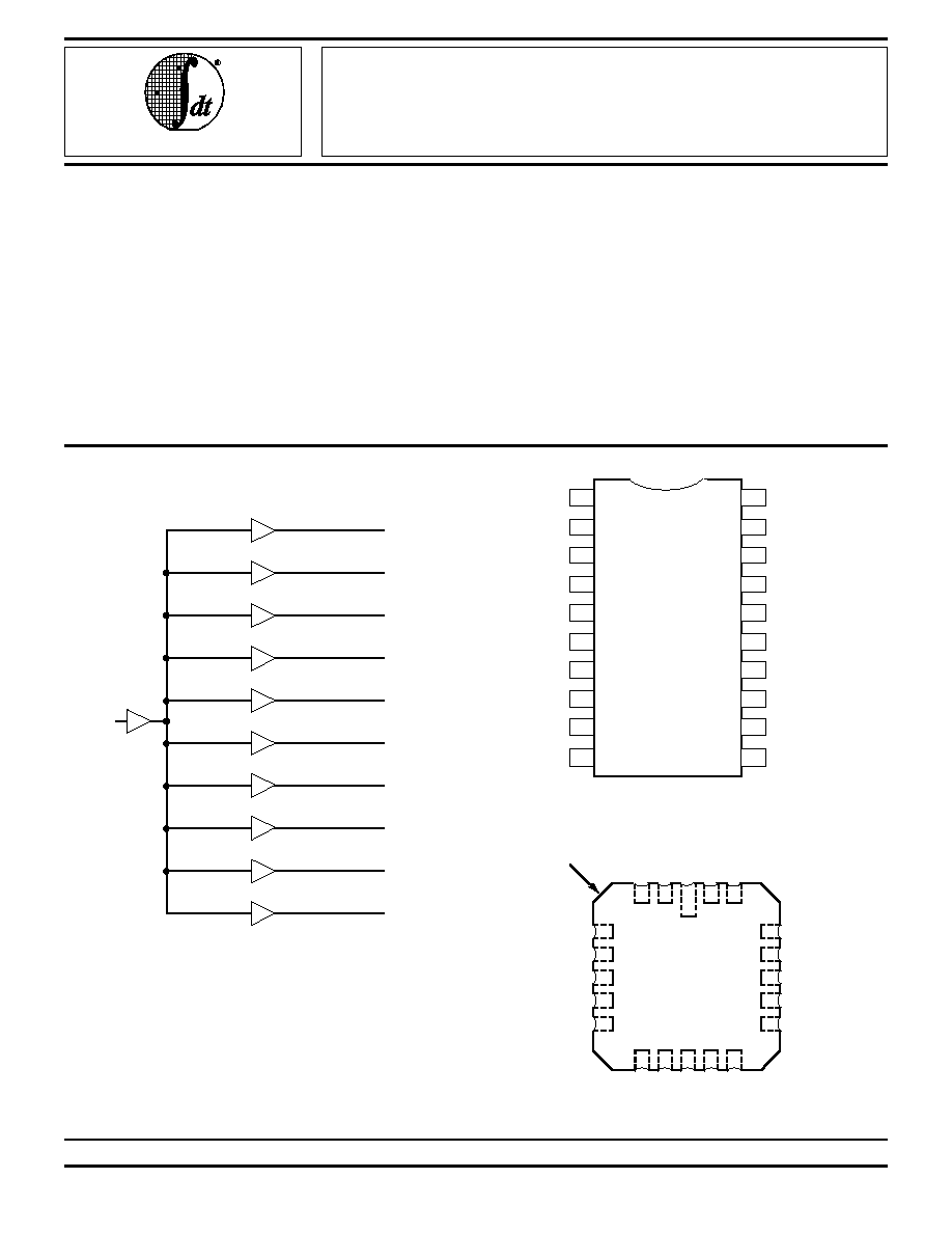
DIP/SOIC/SSOP/QSOP/CERPACK
TOP VIEW
P20-1
D20-1
SO20-2
SO20-7
SO20-8
&
E20-1
IN
O
1
O
2
O
3
O
4
O
10
O
9
O
8
O
7
O
6
INDEX
V
CC
GND
V
CC
GND
V
CC
GND
O
1
IN
V
CC
O
10
O
4
GND
O
5
O
6
GND
LCC
TOP VIEW
O
2
O
3
O
9
O
8
O
7
3
2
20 19
1
4
5
6
7
8
18
17
16
15
14
9 10 11 12 13
L20-2
3017 drw 03
3017 drw 02
DESCRIPTION:
The IDT54/74FCT807BT/CT clock driver is built using
advanced dual metal CMOS technology. This low skew clock
driver features 1:10 fanout, providing minimal loading on the
preceding drivers. The IDT54/74FCT807BT/CT offers low
capacitance inputs with hysteresis for improved noise margins.
TTL level outputs and multiple power and grounds reduce
noise. The device also features -32/48mA drive capability for
driving low impedance traces.
FUNCTIONAL BLOCK DIAGRAM
PIN CONFIGURATIONS
IDT54/74FCT807BT/CT
FAST CMOS 1-TO-10 CLOCK DRIVER
MILITARY AND COMMERCIAL TEMPERATURE RANGES
9.3
2
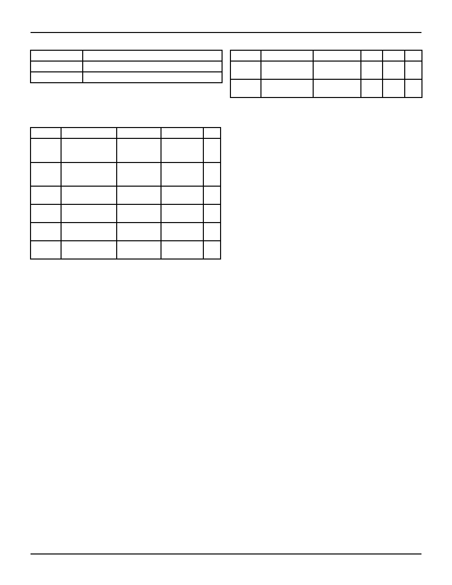
PIN DESCRIPTION
Pin Names
Description
IN
Input
Ox
Outputs
CAPACITANCE
(T
A
= +25
∞
C, f = 1.0MHz)
ABSOLUTE MAXIMUM RATINGS
(1)
3017 tbl 01
Symbol
Parameter
(1)
Conditions
Typ.
Max.
Unit
C
IN
Input
Capacitance
V
IN
= 0V
4.5
6.0
pF
C
OUT
Output
Capacitance
V
OUT
= 0V
5.5
8.0
pF
NOTE:
1. This parameter is measured at characterization but not tested.
3017 lnk 02
Symbol
Rating
Commercial
Military
Unit
V
TERM(2)
Terminal Voltage
with Respect to
GND
≠0.5 to +7.0
≠0.5 to +7.0
V
V
TERM(3)
Terminal Voltage
with Respect to
GND
≠0.5 to V
CC
+0.5
≠0.5 to V
CC
+0.5
V
T
A
Operating
Temperature
0 to +70
≠55 to +125
∞
C
T
BIAS
Temperature
Under Bias
≠55 to +125
≠65 to +135
∞
C
T
STG
Storage
Temperature
≠55 to +125
≠65 to +150
∞
C
I
OUT
DC Output
Current
≠60 to +120
≠60 to +120
mA
3017 lnk 03
NOTES:
1. Stresses greater than those listed under ABSOLUTE MAXIMUM RAT-
INGS may cause permanent damage to the device. This is a stress rating
only and functional operation of the device at these or any other conditions
above those indicated in the operational sections of this specification is not
implied. Exposure to absolute maximum rating conditions for extended
periods may affect reliability. No terminal voltage may exceed V
CC
by
+0.5V unless otherwise noted.
2. Input and V
CC
terminals.
3. Output and I/O terminals.
IDT54/74FCT807BT/CT
FAST CMOS 1-TO-10 CLOCK DRIVER
MILITARY AND COMMERCIAL TEMPERATURE RANGES
9.3
3
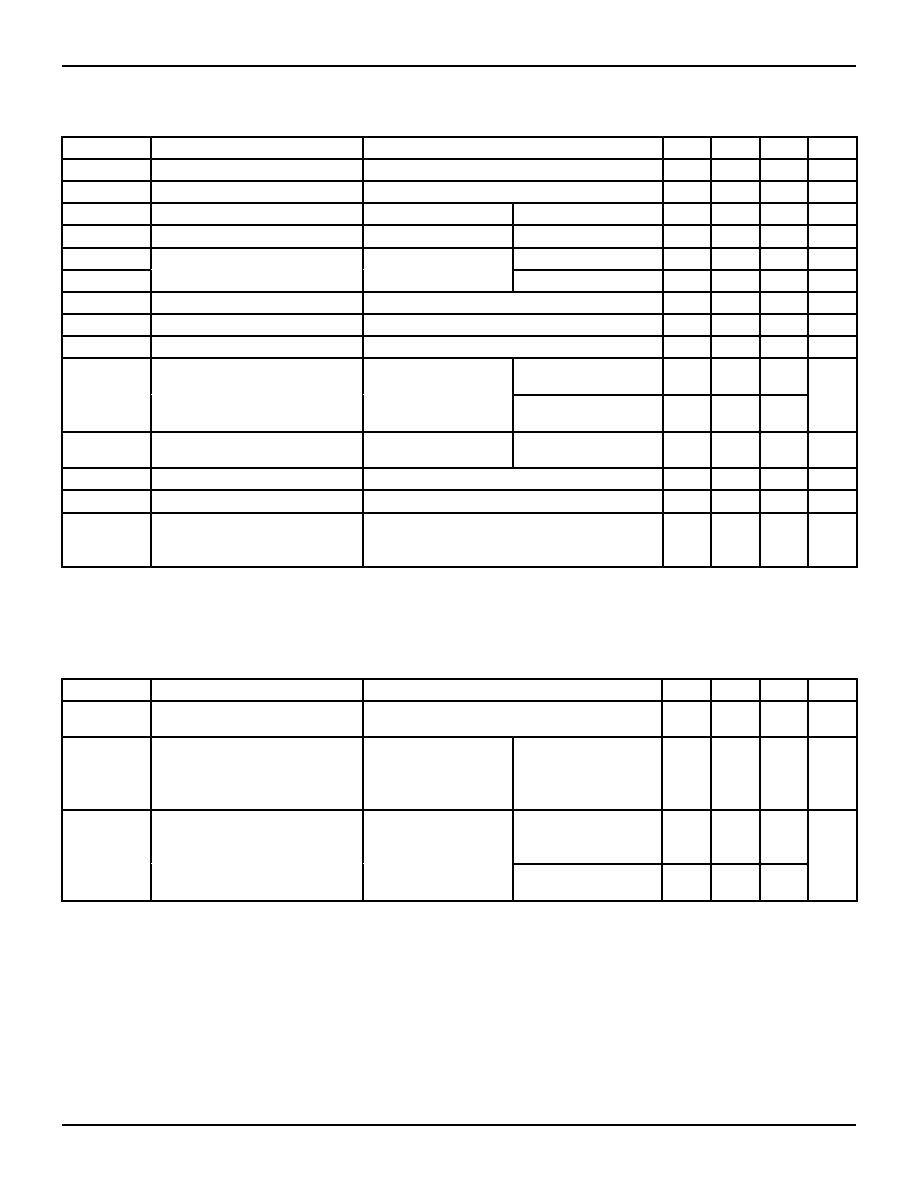
DC ELECTRICAL CHARACTERISTICS OVER OPERATING RANGE
Following Conditions Apply Unless Otherwise Specified
Commercial: T
A
= 0
∞
C to +70
∞
C, V
CC
= 5.0V
±
5%; Military: T
A
= ≠55
∞
C to +125
∞
C, V
CC
= 5.0V
±
10%
NOTES:
1. For conditions shown as Max. or Min., use appropriate value specified under Electrical Characteristics for the applicable device type.
2. Typical values are at Vcc = 5.0V, +25
∞
C ambient.
3. Not more than one output should be tested at one time. Duration of the test should not exceed one second.
4. Duration of the condition can not exceed one second.
5. The test limit for this parameter is
±
5
µ
A at T
A
= ≠55
∞
C.
3017 lnk 04
Symbol
Parameter
Test Conditions
(1)
Min.
Typ.
(2)
Max.
Unit
V
IH
Input HIGH Level
Guaranteed Logic HIGH Level
2.0
--
--
V
V
IL
Input LOW Level
Guaranteed Logic LOW Level
--
--
0.8
V
I
I H
Input HIGH Current
(5)
V
CC
= Max.
V
I
= 2.7V
--
--
±
1
µ
A
I
I L
Input LOW Current
(5)
V
CC
= Max.
V
I
= 0.5V
--
--
±
1
µ
A
I
OZH
High Impedance Output Current
V
CC
= Max.
V
O
= 2.7V
--
--
±
1
µ
A
I
OZL
(3-State Output pins)
(5)
V
O
= 0.5V
--
--
±
1
µ
A
I
I
Input HIGH Current
(5)
V
CC
= Max., V
I
= V
CC
(Max.)
--
--
±
1
µ
A
V
IK
Clamp Diode Voltage
V
CC
= Min., I
IN
= ≠18mA
--
≠0.7
≠1.2
V
I
OS
Short Circuit Current
V
CC
= Max.
(3)
, V
O
= GND
≠60
≠120
≠225
mA
V
OH
Output HIGH Voltage
V
CC
= Min.
V
IN
= V
IH
or V
IL
I
OH
= ≠12mA MIL.
I
OH
= ≠15mA COM'L.
2.4
3.3
--
V
I
OH
= ≠24mA MIL.
I
OH
= ≠32mA COM'L.
(4)
2.0
3.0
--
V
OL
Output LOW Voltage
V
CC
= Min.
V
IN
= V
IH
or V
IL
I
OL
= 32mA MIL.
I
OL
= 48mA COM'L.
--
0.3
0.55
V
I
OFF
Input/Output Power Off Leakage
(5)
V
CC
= 0V, V
IN
or V
O
4.5V
--
--
±
1
µ
A
V
H
Input Hysteresis for all inputs
--
--
150
--
mV
I
CCL
I
CCH
I
CCZ
Quiescent Power Supply Current
V
CC
= Max., V
IN
= GND or V
CC
--
5
500
µ
A
Symbol
Parameter
Test Conditions
(1)
Min.
Typ.
(2)
Max.
Unit
I
CC
Quiescent Power Supply Current
TTL Inputs HIGH
V
CC
= Max.
V
IN
= 3.4V
--
0.5
2.0
mA
I
CCD
Dynamic Power Supply Current
(3)
V
CC
= Max.
Input toggling
50% Duty Cycle
Outputs Open
V
IN
= V
CC
V
IN
= GND
--
0.4
0.6
mA/
MHz
I
C
Total Power Supply Current
(5)
V
CC
= Max.
Input toggling
50% Duty Cycle
V
IN
= V
CC
V
IN
= GND
--
20.0
30.5
(4)
mA
Outputs Open
fi = 50MHz
V
IN
= 3.4V
V
IN
= GND
--
20.3
31.3
(4)
3017 tbl 05
POWER SUPPLY CHARACTERISTICS
NOTES:
1. For conditions shown as Max. or Min., use appropriate value specified under Electrical Characteristics for the applicable device type.
2. Typical values are at V
CC
= 5.0V, +25
∞
C ambient.
3. Per TTL driven input; (V
IN
= 3.4V); all other inputs at V
CC
or GND.
4. This parameter is not directly testable, but is derived for use in Total Power Supply Calculations.
5. Values for these conditions are examples of the I
CC
formula. These limits are guaranteed but not tested.
6. I
C
= I
QUIESCENT
+ I
INPUTS
+ I
DYNAMIC
I
C
= I
CC
+
I
CC
D
H
N
T
+ I
CCD
(f
i
)
I
CC
= Quiescent Current (I
CCL,
I
CCH
and
I
CCZ
)
I
CC
= Power Supply Current for a TTL High Input (V
IN
= 3.4V)
D
H
= Duty Cycle for TTL Inputs High
N
T
= Number of TTL Inputs at D
H
I
CCD
= Dynamic Current Caused by an Input Transition Pair (HLH or LHL)
f
i
= Input Frequency
All currents are in milliamps and all frequencies are in megahertz.
IDT54/74FCT807BT/CT
FAST CMOS 1-TO-10 CLOCK DRIVER
MILITARY AND COMMERCIAL TEMPERATURE RANGES
9.3
4
IDT54/74FCT807BT
IDT54/74FCT807CT
Com'l.
Mil.
Com'l.
Mil.
Symbol
Parameter
Conditions
(1) Min.(2)
Max.
Min.(2)
Max.
Min.(2)
Max.
Min.(2)
Max.
Unit
t
PLH
t
PHL
Propagation Delay
C
L
= 30pF
f
67MHz
1.5
3.8
1.5
3.5
ns
t
R
Output Rise Time
(See figure 3)
--
1.5
--
--
1.5
--
ns
t
F
Output Fall Time
--
1.5
--
--
1.5
--
ns
t
SK
(o)
Output skew: skew between outputs of
same package (same transition)
--
0.5
--
--
0.25
--
ns
t
SK
(p)
Pulse skew: skew between opposite
transitions of same output (|t
PHL -≠
t
PLH
|)
--
0.5
--
--
0.35
--
ns
t
SK
(t)
Package skew: skew between outputs of
different packages at same power supply
voltage, temperature, package type and
speed grade
--
0.9
--
--
0.75
--
ns
3017 tbl 06
3017 tbl 07
3017 tbl 08
NOTES:
1. See test circuits and waveforms.
2. Minimum limits are guaranteed but not tested on Propagation Delays.
3. t
PLH
, t
PHL
, t
SK
(t) are production tested. All other parameters guaranteed but not production tested.
4. Propagation delay range indicated by Min. and Max. limit is due to V
CC
, operating temperature and process parameters. These propagation delay
limits do not imply skew.
SWITCHING CHARACTERISTICS OVER OPERATING RANGE
(3,4)
IDT54/74FCT807BT
IDT54/74FCT807CT
Com'l.
Mil.
Com'l.
Mil.
Symbol
Parameter
Conditions
(1) Min.(2)
Max.
Min.(2)
Max.
Min.(2)
Max.
Min.(2)
Max.
Unit
t
PLH
t
PHL
Propagation Delay
50
to V
CC
/2,
C
L
= 10pF
1.3
2.7
1.3
2.5
ns
t
R
Output Rise Time
(See figure 1)
--
1.5
--
--
1.5
--
ns
t
F
Output Fall Time
or 50
ac
--
1.5
--
--
1.5
--
ns
t
SK
(o)
Output skew: skew between outputs of
same package (same transition)
termination,
C
L
= 10pF
--
0.5
--
--
0.25
--
ns
t
SK
(p)
Pulse skew: skew between opposite
transitions of same output (|t
PHL -≠
t
PLH
|)
(See figure 2)
f
100MHz
--
0.5
--
--
0.35
--
ns
t
SK
(t)
Package skew: skew between outputs of
different packages at same power supply
voltage, temperature, package type and
speed grade
Outputs
connected in
groups of two
--
0.9
--
--
0.65
--
ns
IDT54/74FCT807BT
IDT54/74FCT807CT
Com'l.
Mil.
Com'l.
Mil.
Symbol
Parameter
Conditions
(1) Min.(2)
Max.
Min.(2)
Max.
Min.(2)
Max.
Min.(2)
Max.
Unit
t
PLH
t
PHL
Propagation Delay
C
L
= 50pF
f
40MHz
1.5
3.8
1.5
3.5
ns
t
R
Output Rise Time
(See figure 4)
--
1.5
--
--
1.5
--
ns
t
F
Output Fall Time
--
1.5
--
--
1.5
--
ns
t
SK
(o)
Output skew: skew between outputs of
same package (same transition)
--
0.5
--
--
0.35
--
ns
t
SK
(p)
Pulse skew: skew between opposite
transitions of same output (|t
PHL -≠
t
PLH
|)
--
0.60
--
--
0.45
--
ns
t
SK
(t)
Package skew: skew between outputs of
different packages at same power supply
voltage, temperature, package type and
speed grade
--
1.0
--
--
0.75
--
ns
IDT54/74FCT807BT/CT
FAST CMOS 1-TO-10 CLOCK DRIVER
MILITARY AND COMMERCIAL TEMPERATURE RANGES
9.3
5
TEST CIRCUITS
50
TO V
CC
/2, C
L
= 10pF
Pulse
Generator
R
T
D.U.T.
V
CC
V
IN
C
V
OUT
L
50pF
Pulse
Generator
R
T
D.U.T.
V
CC
V
IN
V
OUT
C
L
30pF
Pulse
Generator
R
T
D.U.T.
V
CC
V
IN
V
OUT
50
10pF
220pF
Pulse
Generator
R
T
D.U.T.
V
CC
V
IN
V
OUT
100
100
10pF
V
CC
Pulse
Generator
R
T
D.U.T.
V
CC
V
IN
C
L
V
OUT
50pF
500
500
7.0V
3017 drw 05
The capacitor value for ac termination is determined by the operating
frequency. For very low frequencies a higher capacitor value should be
selected.
Figure 2.
Figure 1.
3017 drw 06
3017 drw 04
3017 drw 07
3017 drw 08
Figure 4.
Figure 3.
Figure 5.
50
AC TERMINATION, C
L
= 10pF
C
L
= 50pF CIRCUIT
C
L
= 30pF CIRCUIT
ENABLE AND DISABLE TIME CIRCUIT
ENABLE AND DISABLE TIME
SWITCH POSITION
Test
Switch
Disable LOW
Enable LOW
Closed
Disable HIGH
Enable HIGH
Open
DEFINITIONS:
C
L
=
Load capacitance: includes jig and probe capacitance.
R
T
=
Termination resistance: should be equal to Z
OUT
of the Pulse
Generator.
3017 lnk 09
IDT54/74FCT807BT/CT
FAST CMOS 1-TO-10 CLOCK DRIVER
MILITARY AND COMMERCIAL TEMPERATURE RANGES
9.3
6
TEST WAVEFORMS
PACKAGE DELAY
OUTPUT SKEW- t
SK
(o)
PULSE SKEW - t
SK
(p)
PACKAGE SKEW - t
SK
(t)
ENABLE AND DISABLE TIMES
3017 drw 10
3017 drw 09
3017 drw 11
Package 1 and Package 2 are same device type and speed grade
3017 drw 12
t
PLH1
OUTPUT 1
OUTPUT 2
t
SK(o)
t
PLH2
3V
0V
V
OH
1.5V
1.5V
V
OL
V
OH
1.5V
V
OL
INPUT
t
PHL1
t
PHL2
t
SK(o)
3V
0V
V
OH
t
PLH
t
PHL
V
OL
1.5V
1.5V
t
R
t
F
2.0V
0.8V
INPUT
t
PLH1
PACKAGE 1 OUTPUT
PACKAGE 2 OUTPUT
t
SK(t)
t
PLH2
3V
0V
V
OH
1.5V
1.5V
V
OL
V
OH
1.5V
V
OL
t
PHL1
t
PHL2
t
SK(t)
CONTROL
INPUT
3V
1.5V
0V
3.5V
0V
OUTPUT
NORMALLY
LOW
OUTPUT
NORMALLY
HIGH
SWITCH
CLOSED
SWITCH
OPEN
V
OL
V
OH
0.3V
0.3V
t
PLZ
t
PZL
t
PZH
t
PHZ
3.5V
0V
1.5V
1.5V
ENABLE
DISABLE
t
SK(o)
=
|t
PLH2 -
t
PLH1
|
or
|t
PHL2 -
t
PHL1
|
t
PLH
t
PHL
3V
0V
V
OH
1.5V
1.5V
V
OL
t
SK(p)
=
|t
PHL -
t
PLH
|
t
SK(t)
= |t
PLH2 -
t
PLH1
|
or
|t
PHL2 -
t
PHL1
|
INPUT
OUTPUT
INPUT
OUTPUT
3017 drw 13
NOTES:
1. Diagram shown for input Control Enable-LOW and input Control
Disable-HIGH
2. Pulse Generator for All Pulses: f
1.0MHz; t
F
2.5ns; t
R
2.5ns
IDT54/74FCT807BT/CT
FAST CMOS 1-TO-10 CLOCK DRIVER
MILITARY AND COMMERCIAL TEMPERATURE RANGES
9.3
7
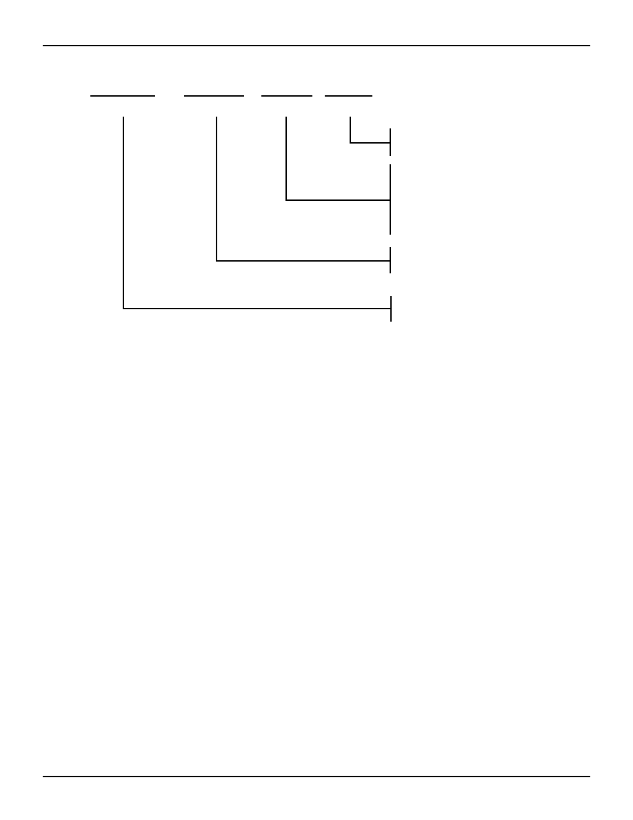
ORDERING INFORMATION
1-to-10 Clock Driver
IDT XX
Temp. Range
XXXX
Device Type
X
Package
X
Process
Blank
B
P
D
SO
L
E
PY
Q
807BT
807CT
Commercial
MIL-STD-883, Class B
Plastic DIP
CERDIP
Small Outline IC
Leadless Chip Carrier
CERPACK
Shrink Small Outline IC
Quarter-size Small Outline IC
54
74
≠55
∞
C to +125
∞
C
0
∞
C to +70
∞
C
FCT
3017 drw 14