Integrated Device Technology, Inc.
MILITARY AND COMMERCIAL TEMPERATURE RANGES
MAY 1992
©
1992 Integrated Device Technology, Inc.
7.19
DSC-4618/2
Æ
IDT54/74FCT821A/B/C
IDT54/74FCT823A/B/C
IDT54/74FCT824A/B/C
IDT54/74FCT825A/B/C
HIGH-PERFORMANCE
CMOS BUS INTERFACE
REGISTERS
FEATURES:
∑ Equivalent to AMD's Am29821-25 bipolar registers in
pinout/function, speed and output drive over full tem-
perature and voltage supply extremes
∑ IDT54/74FCT821A/823A/824A/825A equivalent to
FAST
TM
speed
∑ IDT54/74FCT821B/823B/824B/825B 25% faster than
FAST
∑ IDT54/74FCT821C/823C/824C/825C 40% faster than
FAST
∑ Buffered common Clock Enable (
EN
) and asynchronous
Clear input (
CLR
)
∑ I
OL
= 48mA (commercial) and 32mA (military)
∑ Clamp diodes on all inputs for ringing suppression
∑ CMOS power levels (1mW typ. static)
∑ TTL input and output compatibility
∑ CMOS output level compatible
∑ Substantially lower input current levels than AMD's
bipolar Am29800 series (5
µ
A max.)
∑ Product available in Radiation Tolerant and Radiation
Enhanced versions
∑ Military product compliant to MIL-STD-883, Class B
DESCRIPTION:
The IDT54/74FCT800 series is built using an advanced
dual metal CMOS technology.
The IDT54/74FCT820 series bus interface registers are
designed to eliminate the extra packages required to buffer
existing registers and provide extra data width for wider
address/data paths or buses carrying parity. The IDT54/
74FCT821 are buffered, 10-bit wide versions of the popular
`374 function. The IDT54/74FCT823 and IDT54/74FCT824
are 9-bit wide buffered registers with Clock Enable (
EN
) and
Clear (
CLR
) ≠ ideal for parity bus interfacing in high-perform-
ance microprogrammed systems. The IDT54/74FCT825 are
8-bit buffered registers with all the `823 controls plus multiple
enables (
OE
1
,
OE
2
,
OE
3
) to allow multiuser control of the
interface, e.g.,
CS
, DMA and RD/
WR
. They are ideal for use
as an output port requiring HIGH I
OL
/I
OH
.
All of the IDT54/74FCT800 high-performance interface
family are designed for high-capacitance load drive capability,
while providing low-capacitance bus loading at both inputs
and outputs. All inputs have clamp diodes and all outputs are
designed for low-capacitance bus loading in high-impedance
state.
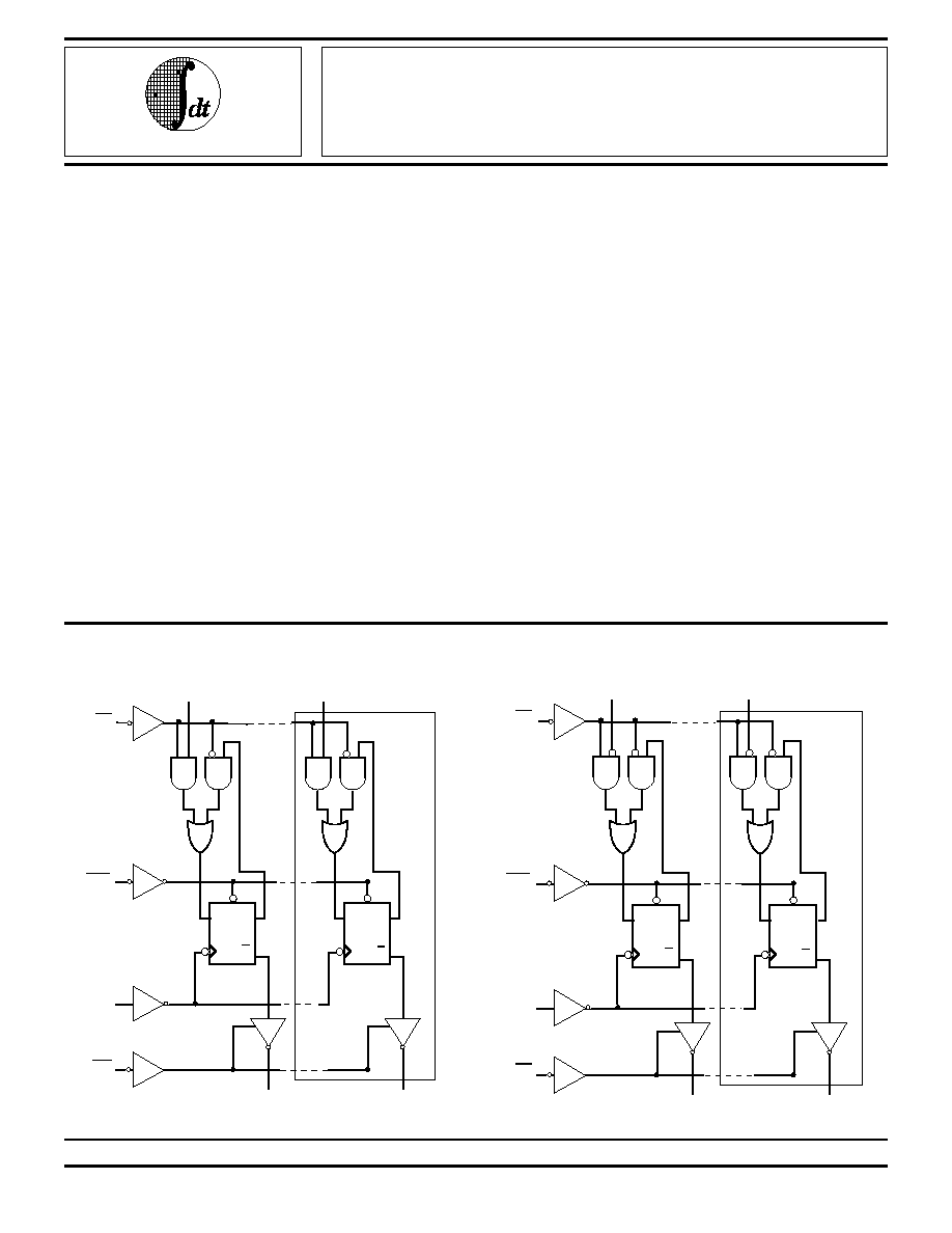
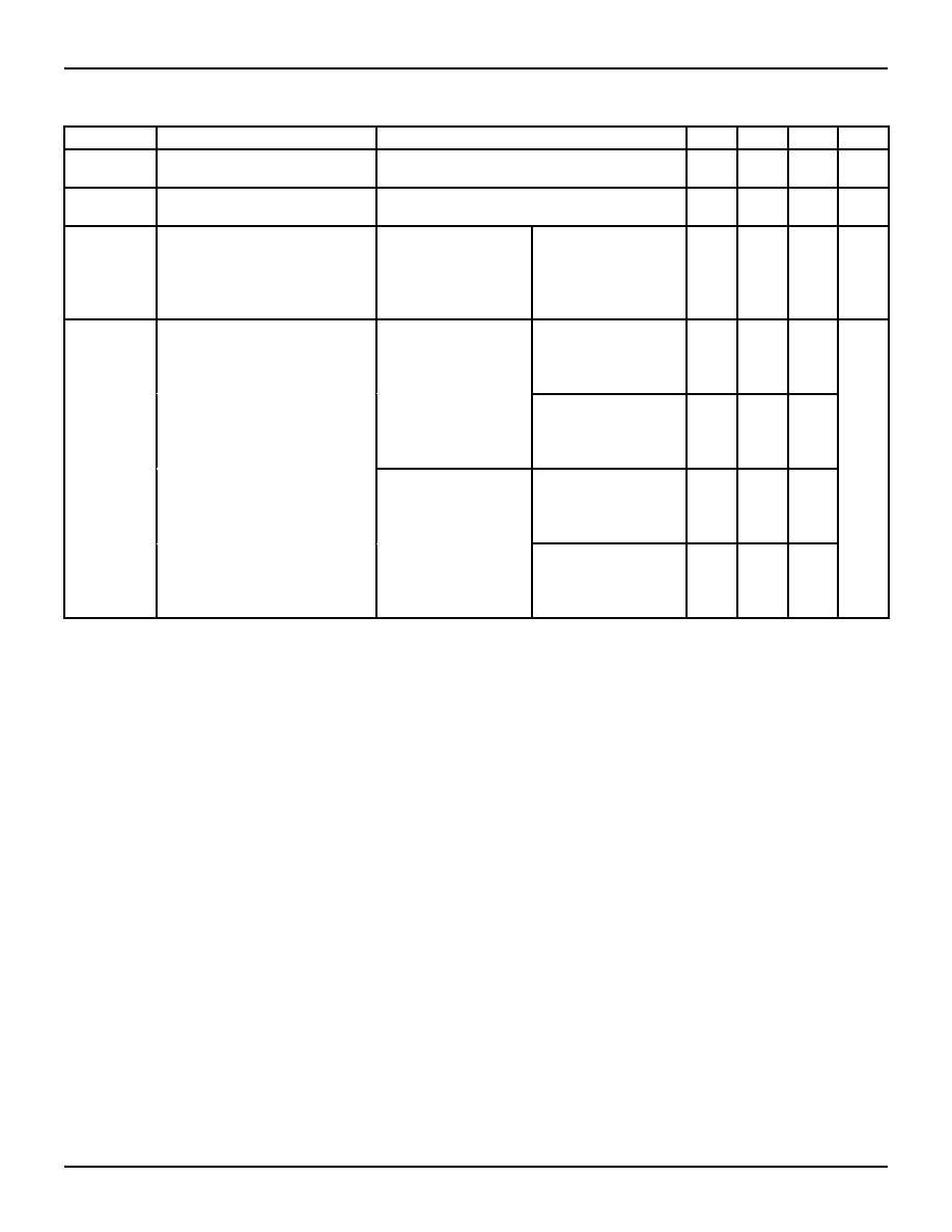
FUNCTIONAL BLOCK DIAGRAMS
IDT54/74FCT821/823/825
IDT54/74FCT824
The IDT logo is a registered trademark of Integrated Device Technology, Inc.
FAST is a trademark of National Semiconductor Co.
2608 cnv* 01
2608 cnv* 02
D
CP Q
Q
CL
D
CP Q
Q
CL
D
0
D
N
Y
0
Y
N
EN
CLR
CP
OE
D
CP Q
Q
CL
D
CP Q
Q
CL
D
0
D
N
Y
0
Y
N
EN
CLR
CP
OE
1
7.19
2
IDT54/74FCT821/823/824/825A/B/C
HIGH-PERFORMANCE CMOS BUS INTERFACE REGISTERS
MILITARY AND COMMERCIAL TEMPERATURE RANGES
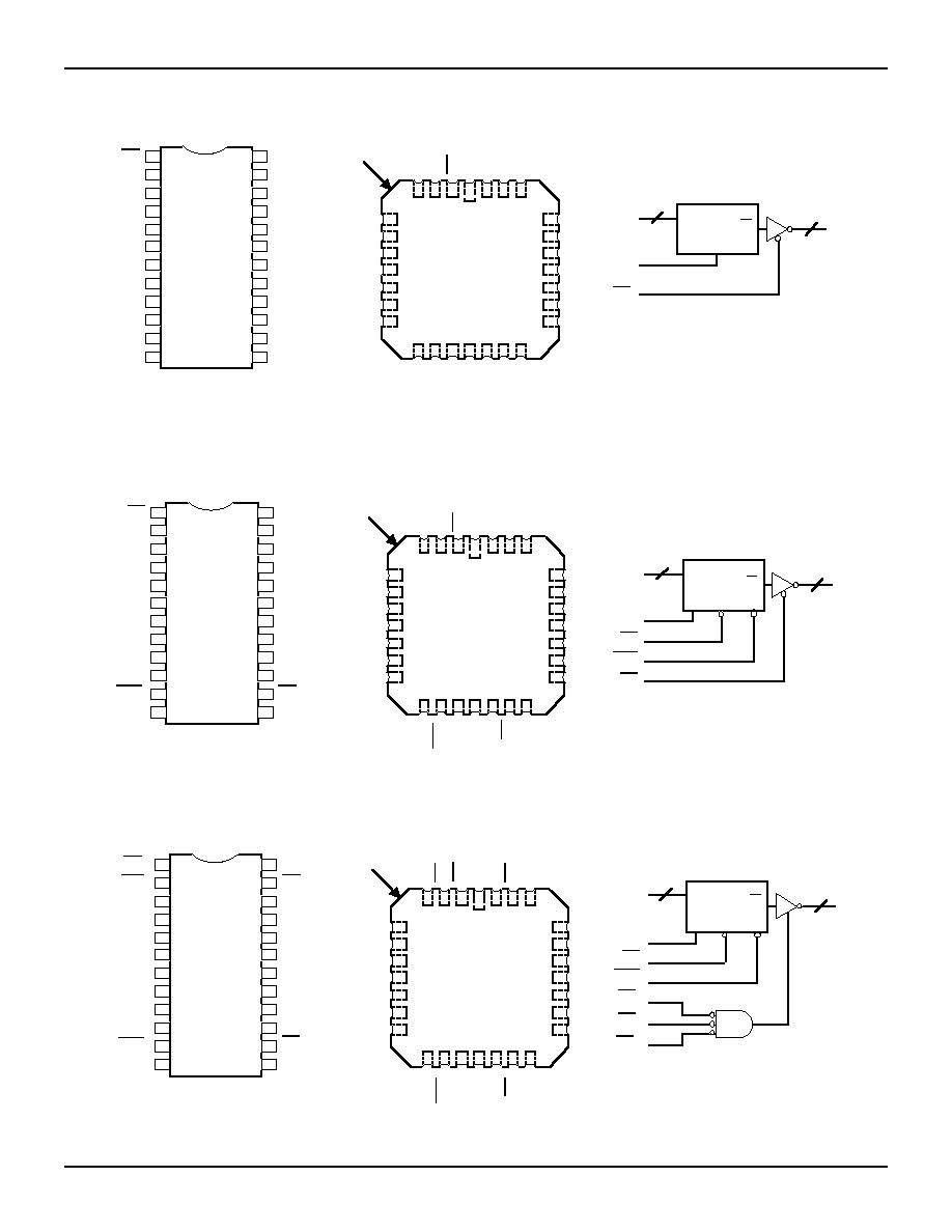
PIN CONFIGURATIONS
LOGIC SYMBOLS
2608 cnv* 03
IDT54/74FCT823/824 9-BIT REGISTERS
IDT54/74FCT825 8-BIT REGISTER
2608 cnv* 04
2608 cnv* 05
IDT54/74FCT821 10-BIT REGISTER
OE
D
0
D
1
D
2
D
3
D
4
D
5
D
6
D
7
GND
Y
0
Y
1
Y
2
Y
3
Y
4
Y
6
CP
Y
5
Y
7
V
CC
1
2
3
4
5
6
7
8
9
10
13
14
15
16
17
18
19
20
P24-1
D24-1
E24-1
&
SO24-2
11
12
21
22
23
24
D
8
D
9
Y
8
Y
9
DIP/SOIC/CERPACK
TOP VIEW
INDEX
D
2
Y
2
Y
3
Y
4
NC
Y
5
OE
D
1
NC
V
CC
Y
0
D
8
GND
CP
Y
9
Y
8
LCC
TOP VIEW
3 2
20
19
1
4
5
6
7
8
18
17
16
15
14
9
10
11
1213
L28-1
D
3
D
4
NC
D
5
D
6
D
7
D
0
Y
1
Y
6
Y
7
21
22
23
24
25
26
27
28
D
9
NC
OE
D
CP
CP
D
Q
Y
10
10
OE
1
D
0
D
1
D
2
D
3
D
4
D
5
D
6
D
7
GND
Y
0
Y
1
Y
2
Y
3
Y
4
Y
6
CP
Y
5
Y
7
V
CC
1
2
3
4
5
6
7
8
9
10
13
14
15
16
17
18
19
20
P24-1
D24-1
E24-1
&
SO24-2
11
12
21
22
23
24
DIP/SOIC/CERPACK
TOP VIEW
INDEX
D
1
Y
1
Y
2
Y
3
NC
Y
4
D
0
NC
V
CC
OE
3
LCC
TOP VIEW
3 2
20
19
1
4
5
6
7
8
18
17
16
15
14
9
10
11
1213
L28-1
D
2
D
3
NC
D
4
D
5
D
6
D
7
GND
CP
EN
Y
7
OE
2
Y
0
Y
5
Y
6
21
22
23
24
25
26
27
28
CLR
NC
OE
1
D
CP
EN
D
Q
Y
8
8
CP
CLR
CLR
EN
OE
2
OE
3
OE
2
CLR
OE
3
EN
OE
1
OE
D
0
D
1
D
2
D
3
D
4
D
5
D
6
D
7
GND
Y
0
Y
1
Y
2
Y
3
Y
4
Y
6
CP
Y
5
Y
7
V
CC
1
2
3
4
5
6
7
8
9
10
13
14
15
16
17
18
19
20
P24-1
D24-1
SO24-2
&
E24-1
11
12
21
22
23
24
D
8
CLR
Y
8
EN
DIP/SOIC/CERPACK
TOP VIEW
INDEX
D
2
Y
2
Y
3
Y
4
NC
Y
5
OE
D
1
NC
V
CC
Y
0
LCC
TOP VIEW
3 2
20
19
1
4
5
6
7
8
18
17
16
15
14
9
10
11
1213
L28-1
D
3
D
4
NC
D
5
D
6
D
7
D
8
GND
CP
EN
Y
8
D
0
Y
1
Y
6
Y
7
21
22
23
24
25
26
27
28
CLR
NC
OE
D
CP
EN
D
Q
Y
9
9
CP
CLR
CLR
EN
IDT54/74FCT821/823/824/825A/B/C
HIGH-PERFORMANCE CMOS BUS INTERFACE REGISTERS
MILITARY AND COMMERCIAL TEMPERATURE RANGES
7.19
3
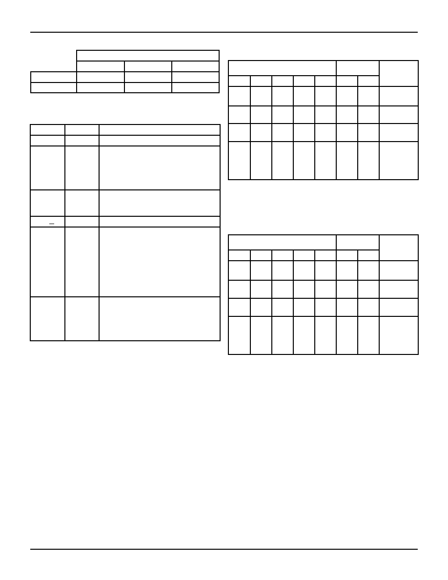
PRODUCT SELECTOR GUIDE
2608 tbl 01
PIN DESCRIPTION
FUNCTION TABLE
(1)
IDT54/74FCT821/823/825
FUNCTION TABLE
(1)
IDT54/74FCT824
2608 tbl 10
Device
10-Bit
9-Bit
8-Bit
Non-inverting
54/74FCT821A/B/C 54/74FCT823A/B/C 54/74FCT825A/B/C
Inverting
54/74FCT824A/B/C
NOTE:
2608 tbl 02
1. H = HIGH, L = LOW, X = Don't Care, NC = No Change,
= LOW-to-HIGH
Transition, Z = High Impedance
NOTE:
2608 tbl 03
1. H = HIGH, L = LOW, X = Don't Care, NC = No Change,
= LOW-to-
HIGH Transition, Z = High Impedance
Name
I/O
Description
D
I
I
The D flip-flop data inputs.
CLR
I
For both inverting and non-inverting
registers, when the clear input is LOW
and
OE
is LOW, the Q
I
outputs are
LOW. When the clear input is HIGH,
data can be entered into the register.
CP
I
Clock Pulse for the Register; enters
data into the register on the LOW-to-
HIGH transition.
Y
I ,
Y
I
O
The register three-state outputs.
EN
I
Clock Enable. When the clock enable
is LOW, data on the D
I
input is
transferred to the Q
I
output on the
LOW-to-HIGH clock transition. When
the clock enable is HIGH, the Q
I
outputs do not change state,
regardless of the data or clock input
transitions.
OE
I
Output Control. When the
OE
input is
HIGH, the Y
I
outputs are in the high
impedance state. When the
OE
input is
LOW, the TRUE register data is
present at the Y
I
outputs.
Inputs
Internal/
Outputs
OE
OE
CLR
CLR
EN
EN
D
I
CP
Q
I
Y
I
Function
H
H
H
H
L
L
L
H
L
H
Z
Z
High Z
H
L
L
L
X
X
X
X
X
X
L
L
Z
L
Clear
H
L
H
H
H
H
X
X
X
X
NC
NC
Z
NC
Hold
H
H
L
L
H
H
H
H
L
L
L
L
L
H
L
H
L
H
L
H
Z
Z
L
H
Load
Inputs
Internal/
Outputs
OE
OE
CLR
CLR
EN
EN
D
I
CP
Q
I
Y
I
Function
H
H
H
H
L
L
L
H
H
L
Z
Z
High Z
H
L
L
L
X
X
X
X
X
X
L
L
Z
L
Clear
H
L
H
H
H
H
X
X
X
X
NC
NC
Z
NC
Hold
H
H
L
L
H
H
H
H
L
L
L
L
L
H
L
H
H
L
H
L
Z
Z
H
L
Load
7.19
4
IDT54/74FCT821/823/824/825A/B/C
HIGH-PERFORMANCE CMOS BUS INTERFACE REGISTERS
MILITARY AND COMMERCIAL TEMPERATURE RANGES
ABSOLUTE MAXIMUM RATINGS
(1)
CAPACITANCE
(T
A
= +25
∞
C, f = 1.0MHz)
NOTE:
2608 tbl 05
1. This parameter is measured at characterization but not tested.
DC ELECTRICAL CHARACTERISTICS OVER OPERATING RANGE
Following Conditions Apply Unless Otherwise Specified: V
LC
= 0.2V; V
HC
= V
CC
≠ 0.2V
Commercial: T
A
= 0
∞
C to +70
∞
C, V
CC
= 5.0V
±
5%; Military: T
A
= ≠55
∞
C to +125
∞
C, V
CC
= 5.0V
±
10%
NOTES:
2608 tbl 06
1. For conditions shown as Max. or Min., use appropriate value specified under Electrical Characteristics for the applicable device type.
2. Typical values are at V
CC
= 5.0V, +25
∞
C ambient and maximum loading.
3. Not more than one output should be shorted at one time. Duration of the short circuit test should not exceed one second.
4. This parameter is guaranteed but not tested.
Symbol
Parameter
(1)
Conditions
Typ.
Max.
Unit
C
IN
Input
Capacitance
V
IN
= 0V
6
10
pF
C
OUT
Output
Capacitance
V
OUT
= 0V
8
12
pF
Symbol
Rating
Commercial
Military
Unit
V
TERM(2)
Terminal Voltage
with Respect to
GND
≠0.5 to +7.0
≠0.5 to +7.0
V
V
TERM(3)
Terminal Voltage
with Respect to
GND
≠0.5 to V
CC
≠0.5 to V
CC
V
T
A
Operating
Temperature
0 to +70
≠55 to +125
∞
C
T
BIAS
Temperature
Under Bias
≠55 to +125
≠65 to +135
∞
C
T
STG
Storage
Temperature
≠55 to +125
≠65 to +150
∞
C
P
T
Power Dissipation
0.5
0.5
W
I
OUT
DC Output
Current
120
120
mA
Symbol
Parameter
Test Conditions
(1)
Min.
Typ.
(2)
Max.
Unit
V
IH
Input HIGH Level
Guaranteed Logic HIGH Level
2.0
--
--
V
V
IL
Input LOW Level
Guaranteed Logic LOW Level
--
--
0.8
V
I
I H
Input HIGH Current
V
CC
= Max.
V
I
= V
CC
--
--
5
µ
A
V
I
= 2.7V
--
--
5
(4)
I
I L
Input LOW Current
V
I
= 0.5V
--
--
≠5
(4)
V
I
= GND
--
--
≠5
I
OZH
Off State (High Impedance)
V
CC
= Max.
V
O
= V
CC
--
--
10
µ
A
Output Current
V
O
= 2.7V
--
--
10
(4)
I
OZL
V
O
= 0.5V
--
--
≠10
(4)
V
O
= GND
--
--
≠10
V
IK
Clamp Diode Voltage
V
CC
= Min., I
N
= ≠18mA
--
≠0.7
≠1.2
V
I
OS
Short Circuit Current
V
CC
= Max.
(3)
, V
O
= GND
≠75
≠120
--
mA
V
OH
Output HIGH Voltage
V
CC
= 3V, V
IN
= V
LC
or V
HC
, I
OH
= ≠32
µ
A
V
HC
V
CC
--
V
V
CC
= Min.
I
OH
= ≠300
µ
A
V
HC
V
CC
--
V
IN
= V
IH
or V
IL
I
OH
= ≠15mA MIL.
2.4
4.3
--
I
OH
= ≠24mA COM'L.
2.4
4.3
--
V
OL
Output LOW Voltage
V
CC
= 3V, V
IN
= V
LC
or V
HC
, I
OL
= 300
µ
A
--
GND
V
LC
V
V
CC
= Min.
I
OL
= 300
µ
A
--
GND
V
LC(4)
V
IN
= V
IH
or V
IL
I
OL
= 32mA MIL.
--
0.3
0.5
I
OL
= 48mA COM'L.
--
0.3
0.5
NOTES:
2608 tbl 04
1. Stresses greater than those listed under ABSOLUTE MAXIMUM
RATINGS may cause permanent damage to the device. This is a stress
rating only and functional operation of the device at these or any other
conditions above those indicated in the operational sections of this
specification is not implied. Exposure to absolute maximum rating
conditions for extended periods may affect reliability. No terminal voltage
may exceed V
CC
by +0.5V unless otherwise noted.
2. Input and V
CC
terminals only.
3. Outputs and I/O terminals only.
IDT54/74FCT821/823/824/825A/B/C
HIGH-PERFORMANCE CMOS BUS INTERFACE REGISTERS
MILITARY AND COMMERCIAL TEMPERATURE RANGES
7.19
5
POWER SUPPLY CHARACTERISTICS
V
LC
= 0.2V; V
HC
= V
CC
≠ 0.2V
NOTES:
2608 tbl 07
1. For conditions shown as Max. or Min., use appropriate value specified under Electrical Characteristics for the applicable device type.
2. Typical values are at V
CC
= 5.0V, +25
∞
C ambient.
3. Per TTL driven input (V
IN
= 3.4V); all other inputs at V
CC
or GND.
4. This parameter is not directly testable, but is derived for use in Total Power Supply Calculations.
5. Values for these conditions are examples of the I
CC
formula. These limits are guaranteed but not tested.
6. I
C
= I
QUIESCENT
+ I
INPUTS
+ I
DYNAMIC
I
C
= I
CC
+
I
CC
D
H
N
T
+ I
CCD
(f
CP
/2 + f
i
N
i
)
I
CC
= Quiescent Current
I
CC
= Power Supply Current for a TTL High Input (V
IN
= 3.4V)
D
H
= Duty Cycle for TTL Inputs High
N
T
= Number of TTL Inputs at D
H
I
CCD
= Dynamic Current Caused by an Input Transition Pair (HLH or LHL)
f
CP
= Clock Frequency for Register Devices (Zero for Non-Register Devices)
f
i
= Input Frequency
N
i
= Number of Inputs at f
i
All currents are in milliamps and all frequencies are in megahertz.
Symbol
Parameter
Test Conditions
(1)
Min.
Typ.
(2)
Max.
Unit
I
CC
Quiescent Power Supply Current
V
CC
= Max.
V
IN
V
HC
; V
IN
V
LC
--
0.2
1.5
mA
I
CC
Quiescent Power Supply Current
TTL Inputs HIGH
V
CC
= Max.
V
IN
= 3.4V
(3)
--
0.5
2.0
mA
I
CCD
Dynamic Power Supply
Current
(4)
V
CC
= Max.
Outputs Open
OE
=
EN
= GND
One Input Toggling
50% Duty Cycle
V
IN
V
HC
V
IN
V
LC
--
0.15
0.25
mA/
MHz
I
C
Total Power Supply Current
(6)
V
CC
= Max.
Outputs Open
f
CP
= 10MHz
50% Duty Cycle
V
IN
V
HC
V
IN
V
LC
(FCT)
--
1.7
4.0
mA
OE
=
EN
= GND
One Bit Toggling
at f
i
= 5MHz
50% Duty Cycle
V
IN
= 3.4V
V
IN
= GND
--
2.2
6.0
V
CC
= Max.
Outputs Open
f
CP
= 10MHz
50% Duty Cycle
V
IN
V
HC
V
IN
V
LC
(FCT)
--
4.0
7.8
(5)
OE
=
EN
= GND
Eight Bits Toggling
at f
i
= 2.5MHz
50% Duty Cycle
V
IN
= 3.4V
V
IN
= GND
--
6.2
16.8
(5)
7.19
6
IDT54/74FCT821/823/824/825A/B/C
HIGH-PERFORMANCE CMOS BUS INTERFACE REGISTERS
MILITARY AND COMMERCIAL TEMPERATURE RANGES
SWITCHING CHARACTERISTICS OVER OPERATING RANGE
NOTES:
2608 tbl* 08
1. See test circuit and waveforms.
2. Minimum limits are guaranteed but not tested on Propagation Delays.
3. This parameter is guaranteed but not tested.
IDT54/74FCT821A/
823A/824A/825A
IDT54/74FCT821B/
823B/824B/825B
IDT54/74FCT821C/
823C/824C/825C
Test
Com'l.
Mil.
Com'l.
Mil.
Com'l.
Mil.
Parameter
Description
Conditions
(1)
Min.
(2)
Max. Min.
(2)
Max. Min.
(2)
Max. Min.
(2)
Max. Min.
(2)
Max. Min.
(2)
Max.
Unit
t
PLH
t
PHL
Propagation Delay
CP to Y
I
(
OE
= LOW)
C
L
= 50pF
R
L
= 500
--
10.0
--
11.5
--
7.5
--
8.5
--
6.0
--
7.0
ns
C
L
= 300pF
(3)
R
L
= 500
--
20.0
--
20.0
--
15.0
--
16.0
--
12.5
--
13.5
t
SU
Set-up Time HIGH or LOW
D
i
to CP
C
L
= 50pF
R
L
= 500
4.0
--
4.0
--
3.0
--
3.0
--
3.0
--
3.0
--
ns
t
H
Hold Time HIGH or LOW
D
I
to CP
2.0
--
2.0
--
1.5
--
1.5
--
1.5
--
1.5
--
ns
t
SU
Set-up Time HIGH or LOW
EN
to CP
4.0
--
4.0
--
3.0
--
3.0
--
3.0
--
3.0
--
ns
t
H
Hold Time HIGH or LOW
EN
to CP
2.0
--
2.0
--
0
--
0
--
0
--
0
--
ns
t
PHL
Propagation Delay,
CLR
to
Y
I
--
14.0
--
15.0
--
9.0
--
9.5
--
8.0
--
8.5
ns
t
REM
Recovery Time
CLR
to CP
6.0
--
7.0
--
6.0
--
6.0
--
6.0
--
6.0
--
ns
t
W
CP Pulse Width
HIGH or LOW
7.0
--
7.0
--
6.0
--
6.0
--
6.0
--
6.0
--
ns
t
W
CLR
Pulse Width
LOW
6.0
--
7.0
--
6.0
--
6.0
--
6.0
--
6.0
--
ns
t
PZH
t
PZL
Output Enable Time
OE
to Y
I
C
L
= 50pF
R
L
= 500
--
12.0
--
13.0
--
8.0
--
9.0
--
7.0
--
8.0
ns
C
L
= 300pF
(3)
R
L
= 500
--
23.0
--
25.0
--
15.0
--
16.0
--
12.5
--
13.5
t
PHZ
t
PLZ
Output Disable Time
OE
to Y
I
C
L
= 5pF
(3)
R
L
= 500
--
7.0
--
8.0
--
6.5
--
7.0
--
6.2
--
6.2
ns
C
L
= 50pF
R
L
= 500
--
8.0
--
9.0
--
7.5
--
8.0
--
6.5
--
6.5
IDT54/74FCT821/823/824/825A/B/C
HIGH-PERFORMANCE CMOS BUS INTERFACE REGISTERS
MILITARY AND COMMERCIAL TEMPERATURE RANGES
7.19
7
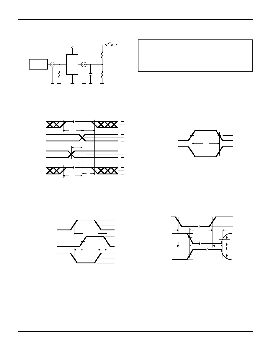
TEST CIRCUITS AND WAVEFORMS
TEST CIRCUITS FOR ALL OUTPUTS
ENABLE AND DISABLE TIMES
PROPAGATION DELAY
SET-UP, HOLD AND RELEASE TIMES
PULSE WIDTH
Pulse
Generator
DATA
INPUT
TIMING
INPUT
ASYNCHRONOUS CONTROL
PRESET
CLEAR
ETC.
SYNCHRONOUS CONTROL
PRESET
CLEAR
CLOCK ENABLE
ETC.
3V
1.5V
0V
3V
1.5V
0V
3V
1.5V
0V
3V
1.5V
0V
t
SU
t
H
t
REM
H
t
SU
R
T
D.U.T.
V
CC
V
IN
C
L
V
OUT
50pF
500
500
7.0V
SAME PHASE
INPUT TRANSITION
3V
1.5V
0V
1.5V
V
OH
V
OL
t
PLH
t
PHL
OUTPUT
OPPOSITE PHASE
INPUT TRANSITION
CONTROL
INPUT
3V
1.5V
0V
3.5V
0V
OUTPUT
NORMALLY
LOW
OUTPUT
NORMALLY
HIGH
SWITCH
CLOSED
SWITCH
OPEN
V
OL
V
OH
3V
1.5V
0V
t
PLH
t
PHL
0.3V
0.3V
t
PLZ
t
PZL
t
PZH
t
PHZ
3.5V
0V
1.5V
1.5V
ENABLE
DISABLE
HIGH-LOW-HIGH
PULSE
LOW-HIGH-LOW
PULSE
t
W
1.5V
1.5V
t
NOTES
2608 drw 01
1. Diagram shown for input Control Enable-LOW and input Control
Disable-HIGH.
2. Pulse Generator for All Pulses: Rate
1.0 MHz; Z
O
50
; t
F
2.5ns;
t
R
2.5ns.
SWITCH POSITION
Test
Switch
Open Drain
Disable Low
Closed
Enable Low
All Other Tests
Open
DEFINITIONS:
2608 tbl 09
C
L
= Load capacitance: includes jig and probe capacitance.
R
T
= Termination resistance: should be equal to Z
OUT
of the Pulse
Generator.
7.19
8
IDT54/74FCT821/823/824/825A/B/C
HIGH-PERFORMANCE CMOS BUS INTERFACE REGISTERS
MILITARY AND COMMERCIAL TEMPERATURE RANGES
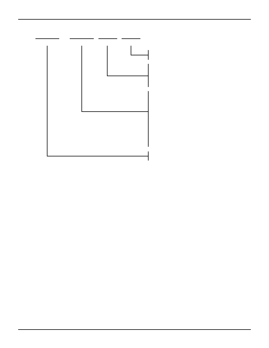
ORDERING INFORMATION
2523 cnv* 11
XX
Temp. Range
XXXX
Device Type
X
Package
X
Process
Blank
B
P
D
E
L
SO
821A
821B
821C
823A
823B
823C
824A
824B
824C
825A
825B
825C
Commercial
MIL-STD-883, Class B
Plastic DIP
CERDIP
CERPACK
Leadless Chip Carrier
Small Outline IC
10-Bit Non-Inverting Register
Fast 10-Bit Non-Inverting Register
Super Fast 10-Bit Non-Inverting Register
9-Bit Non-Inverting Register
Fast 9-Bit Non-Inverting Register
Super Fast 9-Bit Non-Inverting Register
9-Bit Inverting Register
Fast 9-Bit Inverting Register
Super Fast 9-Bit Inverting Register
8-Bit Non-Inverting Register
Fast 8-Bit Non-Inverting Register
Super Fast 8-Bit Non-Inverting Register
54
74
≠55
∞
C to +125
∞
C
0
∞
C to +70
∞
C
FCT
IDT
2608 cnv* 11